Chemical Vapor Deposition of Conjugated Polymeric
Thin Films for Photonic and Electronic Applications
by
John Patrick Lock
Master of Science, Chemical Engineering Practice
Massachusetts Institute of Technology, Cambridge, Massachusetts, 2005 Bachelor of Science, Chemical Engineering
University of Colorado at Boulder, 1998 Subitted to the Department of Chemical Engineering in Partial Fulfillment of the Requirements for the Degree of DOCTOR OF PHILOSOPHY IN CHEMICAL ENGINEERING
at the
MASSACHUSETTS INSTITUTE OF TECHNOLOGY June 2005
© 2005 Massachusetts Institute of Technology. All rights reserved.
(n '
ii
Signature of Author:
Certified by:
Accepted by:
...
Department of Chemical EngineeringMay 12, 2005
?
Karen K Gleason Professor of Chemical Engineering Thesis Advisor
MASSACHUSETTS INS11TUTE
OF TECHNOLOGY
SEP 1 2 205
Daniel Blankschtein Professor of Chemical Engineering Chairman, Committee for Graduate Students
Chemical Vapor Deposition of Conjugated Polymeric
Thin Films for Photonic and Electronic Applications
by
John Patrick Lock
Submitted to the Department of Chemical Engineering on May 13, 2005 in Partial Fulfillment
of the Requirements for the Degree of Doctor of Philosophy in Chemical Engineering
Abstract
Conjugated polymers have delocalized electrons along the backbone, facilitating electrical conductivity. As thin films, they are integral to organic semiconductor devices emerging in the marketplace, such as flexible displays and plastic solar cells, as well as next-generation microphotonic chips. A major processing challenge is that these materials are relatively insoluble. Chemical vapor deposition (CVD) is presented as a synthesis technique for conjugated polymers as an alternative to electrochemical and liquid dispersion methods. CVD will continue to be an essential component of the materials toolset for manufacturers of
semiconductor devices.
Polysilanes, with a backbone consisting of silicon atoms instead of carbon, have delocalized electrons due to the presence of d-orbitals. Plasma-enhanced CVD (PECVD) of polysilane films was achieved, but they did not exhibit electrical conductivity. Branching resulting from the energetic plasma process quenches the conjugation. However, photo
oxidation was used to convert Si-Si bonds into Si-O-Si, reducing the refractive index up to 5%. This led to the direct patterning of tunable waveguides in PECVD hexamethyldisilane (6M2S). Other essential devices for microphotonics are microring resonators used for filtering an individual wavelength from "multicolor" light. Photo oxidation of 6M2S, deposited as the cladding material on ring resonators, allows one to shift the resonant wavelength an order of
magnitude more than conventional thermal trimming techniques. Microphotonics will ultimately increase computing speeds with chips that operate using light instead of electricity.
A CVD technique was also developed for poly-3,4-ethylenedioxythiophene or PEDOT. Among conducting polymers, PEDOT has superior conductivity (up to 300 S/cm) and excellent stability. CVD PEDOT has a conductivity of about 5 S/cm, while 1 S/cm is the figure-of-merit for a good conducting polymer film. As a charge-injecting layer in organic light-emitting diodes (OLEDs), PEDOT increases the overall power efficiency 30-50%. CVD can further enhance this efficiency gain in organic devices by more conformally coating PEDOT on high-area surfaces. CVD PEDOT films also exhibit reversible electrochromic behavior changing color from their as-deposited sky blue color to a darker blue when they are reduced with an applied volatage. A 50-nm film had a contrast of 16.5% with a switching speed of 27 ms.
Thesis Supervisors: Karen K Gleason
To Andrea, Mom, and Loreen
Acknowledgments
I can't thank enough all the people who have enabled my thesis research during my time at MIT. I have had the great fortune of being supported along the way by the most generous family, friends, mentors, and advisors.
I'd like to thank my advisor, Karen, a truly extraordinary scientist. More often than not, her outlook concerning the likelihood of success for a given experiment has been right on. While allowing me the freedom to explore all of my ideas, she is responsible for providing an overall direction to my project, which I feel has optimized the impact it has achieved.
Professors Vladimir Bulovi6, Paula Hammond, and Bill Green were the members of my thesis committee. I thank them for their time, encouragement, and advice throughout the years. It was great having access to such a store of knowledge in their areas of expertise. In addition, I would like to thank Professor Kimerling and Jurgen Michel for all of their ideas.
The materials side of my project happened mainly in the Gleason Lab alongside a very stimulating group of people to share office and lab space with. Thank you to all of the Gleason Group members. However, the majority of my results have been the demonstration of my materials in a variety of functional devices, all of which were made in collaboration with a number of other labs across campus. For their help, I would like to thank the following: Dan Sparacin and Jessica Sandland in the Kimerling Lab, Jodie Lutkenhaus and Nicole Zacharia in the Hammond Lab, Jen Yu and Jonathon Tischler in the Bulovi6 Lab, Angela Chen and Rachel Pytel in the Swager and Hunter Labs, and Tetsuo Sato in the Yokoyama Lab and the University
In addition to all of the students at MIT that I have collaborated with for my research, I have worked closely with many more through all of the extracurricular activities that have shaped my overall graduate school experience. First I'd like to thank the members of Advanced Conductors for the great run in the $50K and the Ignite Clean Energy Competition. Thanks Karl, Sam, Steve, and Pete - maybe next year! I'd also like to say cheers to all of the Muddy bartenders. Finally I'd like to acknowledge all the fellow members of the GSC, TechLink, and TinyTech.
The companionship of my friends provided me with so much happiness and many unforgettable experiences - thanks especially to Steve, Kelvin, April, and all of the winos. Thanks also to the KFJ group for all of the lunchtime conversations.
I really appreciate the outpouring of support that has always been a constant in my life from Mom, Loreen, my grandparents, and all of my aunts, uncles, and cousins.
Finally, I love you, Andrea. Thank you for being a constant source of support and for providing such a fine example whenever I need someone to emulate. You've motivated me to run marathons, be Catholic, and now finish my PhD. I look forward to our life together and I'll try to be as much an inspiration for you as you have been for me.
TABLE OF CONTENTS
Abstract
Dedication 3 Acknowledgments 4 List of Figures 9 List of Tables 13List of Notations
14
CHAPTER ONE 1 7 Introduction 1.1 Motivation 181.2 c-Conjugated Polymers: Polysilanes 19
1.2.1 Electrical Properties of Polysilanes 20
1.2.2 Photolability of Polysilanes 22
1.2.3 Synthesis Techniques 24
1.3 v-Conjugated Polymers: PEDOT 25
1.3.1 Synthesis Techniques 27
1.4 Outlook: 28
1.5 Thesis Framework 28
CHAPTER TWO 36
Tunable Waveguides via Photo Oxidation of Plasma Polymerized Organosilicon Films
Abstract 37
2.1 Introduction 38
2.2 Experiment 42
2.3 Results and Discussion 44
2.3.1 UV Irradiation of PECVD Organosilicon Films 44
2.3.2 Coupling and Tuning of Slab Mode Waveguides 46
CHAPTER THREE 53
Trimming of Microring Resonators Using Photo-Oxidation of a Plasma-Polymerized
Organosilane Cladding Material
Abstract 54 3.1 Introduction 55 3.2 Experiment 57 3.3 Discussion 59 3.3.1 Ring Theory 59 3.3.2 Characterization of CVD Films 59 3.4 Results 62 3.5 Conclusions 66 References 67 CHAPTER FOUR
69
Chemical Vapor Deposition of Thin Films of Electrically Conducting PEDOT
Abstract 70
4.1 Introduction 71
4.2 Background 73
4.2.1 Mechanism for the Oxidative Polymerization of PEDOT 73
4.3 Experiment 77
4.4 Results and Discussion 79
4.5 Conclusion 83
References 85
CHAPTER FIVE 89
Electrochemical Investigation of PEDOT Thin Films Deposited Using CVD as a Candidate Material for Organic Memory and Electrochemical Applications
Abstract 90
5.1 Introduction 91
5.2 Experiment 93
5.3 Discussion and Results 95
5.3.1 Cyclic Voltammetry 95
5.3.2 UV/Vis Spectroscopy 97
5.3.3 Chrono Amperommetry 97
5.4 Conclusions 104
CHAPTER SIX
Conclusions
CHAPTER SEVEN
Future Directions
APPENDIX A
Structural Differences Between CVD and Spin-On Polysilane Films
Objective
A.1 Introduction
A.2 Synthesis of Polysilane Films
A.2.1 Chemical Vapor Deposition
A.2.2 Spin-On Deposition
A.3 CVD and Spin Coating Processing Considerations A.4 Chemical Composition
A.5 Stability
A.6 UV/Vis Absorption A.7 Photo Oxidation A.8 Thermochromism A.9 Proposed Structure A. 10 Proposed Applications
109
112
116
117 118 118 118 119 120 122 123 125 126 128 130 132List of Figures
CHAPTER ONE
Figure 1-1: Molecular repeat unit of a polysilane.
Figure 1-2: Schematic showing the geminal and vicinal interactions between sp3 orbitals in a
ac-conjugated linear chain of catenated Si atoms.
Figure 1-3: Conjugated polymers have delocalized electrons that split discreet molecular orbital
energies into bands that are analogous to the conducting and valence bands of semiconductors.
Figure 1-4: E xposure to UV light converts a polysilane network into a polysiloxane material.
Figure 1-5: Direct irradiation of polysilanes with UV light can be used to define low index regions in
the material, which can be useful for patterning optical devices.
Figure 1-6: Common conducting polymers include (a) polyacetylene, (b) polypyrrole, (c)
polyaniline, (d) polyphenylenevinylene, (e) polythiophene, and (f)
poly-3,4-diethylenedioxythiophene (PEDOT).
CHAPTER TWO
Figure 2-1: Photo oxidation occurs via an insertion reaction when an Si-Si bond is irradiated with UV
light. This decreases the molecular density of the material and reduces the refractive
index. R and R2are organic substituents (ie methyl, phenyl, etc).
Figure 2-2: Schematic of the prism coupling technique for measuring optical properties of light
guiding films.
Figure 2-3: Contrast curve for a plasma polymerized dimethylsilane film irradiated with 193 nm
light. A maximum refractive index contrast of 0.05 or 3% was achieved with a dosage of
900 mJ/cm2.
Figure 2-4: Contrast curve for a plasma polymerized hexamethyldisilane film irradiated with a Hg arc
lamp.
Figure 2-5: a) Two modes of 633 nm light are coupled into this 0.79 [tm thick plasma polymerized
Figure 2-6: a) Two modes can be supported by a 0.79 ptm film of 6M2S. b) One mode of 1550 nm light can be coupled to this film.
Figure 2-7: For the 6M2S sample with 0.79 [um thickness, the refractive index would have to be
decreased slightly by 0.01 or 1% to have single mode performance at both 633 nm (a) and 1550 nm (b).
Figure 2-8: Prism coupling measurements after UV irradiation confirm tunability of 6M2S film. The
6 M2S now has single-mode performance for both 633 nm'(a) and 1550 nm (b).
CHAPTER THREE
Figure 3-1: Schematic of a ring resonator device.
Figure 3-2: .JV irradiation causes scission of Si-Si bonds allowing oxygen incorporation, which
lowers the refractive index of the material.
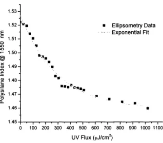
Figure 3-3: Fitting the Cauchy-Urbach model to ellipsometry data yields the thickness and optical
constants of plasma polymerized 6M2S films.
Figure 3-4: Reasonable agreement is seen between refractive index contrast results at 1550 nm
collected using an ellipsometer operating in the visible range (450 to 720 nm) and an ellipsometer operating in the near-IR (800 to 1750 nm).
Figure 3-5: The refractive index of PECVD 6M2S cladding material decreases with UV irradiation as
a result of photo-oxidation.
Figure 3-6: 1-M mode spectral measurements of a 100 jlm Si3N4 ring resonator (.,1=1564.5 nm)
after 300 and 420 seconds of UV irradiation at 1.7 [tW/cm 2.
Figure 3-7: The experimental resonance shifts for TE and TM polarizations are compared with
modeled results.
CHAPTER FOUR
Figure 4-1: Diaz mechanism for oxidative polymerization.
Figure 4-2: Neutral PEDOT is oxidized to form a conducting polycation that is charge balanced with
dopant anions.
Figure 4-3: Acid-initiated coupling promotes chain growth.
Figure 4-5: Schematic of CVD reactor for depositing PEDOT films.
Figure 4-6: FTIR spectra and conductivity values for CVD PEDOT and standard PEDOT films.
Figure 4-7: Comparison of PEDOT polymerized in the presence of pyridine before and after
methanol rinse.
Figure 4-8: Pyridine readily reacts with HCI to form a pyridinium salt.
CHAPTER FIVE
Figure 5-1: Neutral PEDOT is oxidized to form a conducting polycation that is charge balanced with
dopant anions. Oxidized PEDOT has a transparent light blue color that turns dark purple upon reduction.
Figure 5-2: A schematic of a CVD process for the deposition of PEDOT
Figure 5-3: Cyclic voltammetry indicates that PEDOT is reduced gradually, but oxidizes more
suddenly. This stems from the conductivity of oxidized PEDOT as opposed to the
non-conducting reduced form.
Figure 5-4: UIV/Vis spectroscopy indicates that CVD PEDOT has a maximum color contrast of
16.5% at a wavelength of 585 nm.
Figure 5-5: A square wave form with a step time of 500 msec and potential limits of 400 mV and
-600 mV was chosen for chrono amperommetry measurements.
Figure 5-6: A CVD PEDOT film 50 nm thick has a swiching speed of about 50 msec for a 90%
change and is as low as 27 msec for an 80% response.
Figure 5-7: The charge response of a CVD PEDOT film is proportional to t 2 indicating a
diffusion-controlled process.
Figure 5-8: Chrono amperommetry data is condensed into an Anson plot that is useful for calculating
diffusion constants for charge transfer processes. CVD PEDOT has a diffusion
coefficient on the order of 10-1 cm2/s indicating that the process is controlled by ion
APPENDIX A
Figure A-I: Schematic diagram of PECVD reactor. RF energy introduced to the top electrode
induces a plasma between the two capacitively coupled electrodes.
Figure A-2: FTIR spectra of CVD polydimethylsilane films are compared with a CVD organosilicon
film and a commercially produced polydimethylsilane powder. Oxygen has not yet been eliminated, but there is a progressive decline in the oxygen content of CVD polydimethylsilane films.
Figure A-3: FTIR CVD polysilane materials are stable to oxidation over time in normal laboratory
conditions. This sample was stored for over two weeks in atmosphere under room
lighting.
Figure A-4: CVD polysilane films show good chemical stability compared to spin-on polysilanes.
Figure A-5: .JV/Vis spectra show absorption due to ,c-conjugation for spin-on PMPS films at 333 nm.
No corresponding peak is seen for analogous CVD films.
Figure A-6: Photo oxidation occurs via an insertion reaction when an Si-Si bond is irradiated with UV
light. This decreases the molecular density of the material and reduces the refractive index.
Figure A-7: An increase in the Si-O peak in the FTIR spectrum for a plasma polymerized
climethylsilane film demonstrated photo oxidation of Si-Si bonds with UV irradiation.
Figure A-8: Absorption of NIR light transforms polysilane chains to a random helix conformation.
1-his interrupts -conjugation, which decreases the refractive index. This is a reversible
transformation.
Figure A-9: Thermochromism in spin-on polysilane films evident by swelling and a reduction in the
refractive index is largely absent in analogous CVD materials.
Figure A-10: A comparison of spin-on and CVD polysilane films indicates a more conjugated
backbone for the spin-on material. Branching and unsaturated silicon atoms are among the characteristics expected for the amorphous CVD films.
List of Tables
CHAPTER FOUR
List of Acronyms, Abbreviations, and Symbols
Roman Acronyms and Abbreviations
2MS 2EthS 6M2S A An-Cn BAYTRON C BAYTRON M BAYTRON P C,* C-Band CA C:V CVD CVD 1-4 dn/dT 1)3 I)o I)C I:)CS EDOT E, EI 1-2 eV F FSR FTIR HOMO HPLC I IR ITO k L-Band LCD LEDs LPCVD LUMO mn MEMS NIPS Dimethylsilane Diethylsilane Hexamethyldisilane Area Cauchy Coefficients
Bayer Chemicals Product (Catalyst) Bayer Chemicals Product (Monomer) Bayer Chemicals Product (Polymer) Concentration of Reacting Species in Film Wavelengths Between 1530 and 1565 nm Chrono Amperommetry
Cyclo Voltammetry
Chemical Vapor Deposition
PEDOT Films Deposited with CVD Thermo-Optic Coefficient of Materials Hexamethylcyclotrisiloxane
Diameter of Microring Diffusion Constant Direct Current Direct Current Source 3,4-ethylenedioxythiophene Voltage Potential
Bounding Potentials of Cyclovoltammogram Oxidation Peak Electron Volt
Faraday's Constant
Free Spectral Range
Fourier Transform Infrared Spectroscopy Highest Occupied Molecular Orbital High Pressure Liquid Chromatography Current
Infrared
Indium Tin Oxide Boltzmann Constant
Wavelengths Between 1565 and 1610 nm Liquid Crystal Display
Light-Emitting Diodes
Low Pressure Chemical Vapor Deposition Lowest Unoccupied Molecular Orbital Resonant Mode Number
Micro Electro Mechanical Systems Methylphenylsilane
n Refractive Index
ln Effective Refractive Index of Microring Resonator
ln Charge Difference Between Reduced and Oxidized Species
NIR Near Infrared
OLEDS Organic Light-Emitting Diodes
PANI Polyaniline
-PDA Personal Digital Assistant
PDHS Poly-dihexylsilane
PDMS Poly-dimethylsilane
PECVD Plasma-Enhanced Chemical Vapor Deposition
PEDOT Poly-3,4-ethylenedioxythiophene
PMPS Poly-methylphenylsilane
PPV Poly-phenylenevinylene
PSS Poly-styrene Sulfonic Acid
Q Charge
R Organic Sidegroup Constituent (ie Methyl, Phenyl, etc)
rf Radio Frequency
S Slope From the Anson Plot
S/cm Siemens/cm (Units of Bulk Conductivity)
sccm Standard Cubic Centimeters per Minute
SCE Standard Calomel Electrode
SMF Single Mode Fiber
TE Transverse Electric Polarization of Light
THF Tetrahydrofuran
1TM Transverse Magnetic Polarization of Light
TMAH Tetramethylammonium Hydroxide
to Experiment Start Time
Tg Glass Transition Temperature
UJV Ultraviolet Light
UV/Vis Ultraviolet and Visible Light
VASE Variable Angle Spectroscopic Ellipsometry
Greek Symbols
Film Thickness
C Sigma Bond
0(Film Incident Angle of Light Inside Film
;t Free Space Wavelength of Light
3.0 Free Space Wavelength of Resonant Light
Free Space Wavelength of Resonant Light Before Irradiation
ko,2 Free Space Wavelength of Resonant Light After Irradiation
(Air Goos-Haenchen Shift at Air/Film Interface
(Substrate Goos-Haenchen Shift at Substrate/Film Interface
,!X Shift in Resonant Wavelength
13/k Speed of Light in Vacuum / Speed of Light Propagation in Film
v Scan Rate of Cyclovoltammetry Experiment
: Pi Bond
Chapter One
1.1 MOTIVATION
In 1977, the field of conducting polymeric materials, also known as synthetic metals, began with the discovery that polyacetylene conducts electricityl, earning the Nobel Prize in Chemistry in 2000 for Alan Heeger, Alan MacDiarmid, and Hideki Shirakawa. Recent reviews examine numerous efforts to incorporate conducting polymers into an increasing number of electronic devices including light-emitting diodes (LEDs)2 ' 3, electrochromic materials and structures4, microelectronics5 6, portable and large-area displays7, and photovoltaics8. Just as, "everything that can go digital will go digital", traditional semiconductor devices that we use every day including computers, cell phones, PDAs, and solar cells, will transition into less expensive and more disposable organic or plastic forms. Not to be confused with biological materials, organic simply refers to carbon-based materials as opposed to traditional inorganic semiconductors. Benfits of this transition will be realized over time: new and flexible device forms, thin and light-weight components, and energy efficiency gains amounting to about 10% of the current US electricity demand. The advent of organic electronic devices and the propensity for everything to shrink to the nano scale will facilitate a future of increased convenience and capability with the evolution of technology.
Conjugated polymers will become increasingly important as active materials in next-generation electronic devices. Conjugated polymers have delocalized electrons along their backbones enabling charge conduction. They include polyphenylene, polyaniline, polythiophene, polypyrrole, polycarbazole, and polysilane, among others. Each of these families of polymers can be substituted with a variety of functional groups to achieve different properties, and new derivatives continue to be synthesized and studied9' 10
1.2
a-CONJUGATED POLYMERS: POLYSILANESPolysilanes are polymers composed of catenated silicon atoms that form a linear chain". An example of a polysilane molecular repeat unit is shown in Figure 1-1:
Si
Figure 1-1: Molecular repeat unit of a polysilane.
where R1 and R2 are carbon-based ligands, such as methyl or phenyl groups. Excellent thermal and mechanical properties of these materials, coupled with their unusual electronic characteristics and photolability, have led to many applications including their use as a photoresist, as a nonlinear optical material for electro optic applications, and as an active conducting, photoconducting, or charge transporting layer in electronic devices2. The first of these materials was probably made in the early 1920's 3' 14. However, the highly crystalline material attracted little scientific interest because it was generally insoluble and intractable. In the past 30 years, polysilanes have been rediscovered and modem techniques have been applied to their characterization. It seems likely that the future will bring new breakthroughs in the understanding and development of polysilanes; and, new synthetic procedures remain an important priority in this field'2.
1.2.1 ELECTRICAL PROPERTIES OF POLYSILANES
Instead of having conjugated, aromatic, ni-bonding like the majority of conducting polymers, polysilanes depend on delocalized a-bonding". The exact mechanism of electron delocalization in a-conjugated systems is unclear. Overlapping d orbitals are available to silicon atoms and likely play a role although the antibonding C bonds in silicon polymers are thought to be of a low enough energy to contribute to delocalization as well. Figure 1-2 depicts a polysilane segment in its all trans zigzag conformation.
Figure 1-2: Schematic showing the geminal and vicinal interactions between sp3orbitals in a c-conjigated linear chain of catenated Si atoms.
The interaction of vicinal orbitals produces a splitting into bonding HOMO (highest occupied molecular orbitals) and antibonding LUMO (lowest unoccupied molecular orbitals)". If there were only vicinal orbital interactions and no geminal orbital interactions, the electrons would be completely localized between the Si atoms and the HOMO and LUMO energy levels would be very sharp and distinct. However, with increasing geminal orbital interactions, there is delocalization of the electrons and a splitting of each of the polymeric HOMO and LUMO levels
to yield bands. An optical energy gap between 1.5 and 3eV exists between the HOMO and LUMO energy levels of polysilanes'5. Many polsilanes are very transmissive in the visible region and absorb primarily UV light16.
LUMO
"IAl
LUMO <
-
t--
I
A,Eg
1HOMO
<HOMO
Polymeric
Atomic
Molecular
Molecular
sp
3Orbitals
Orbitals
Orbitals
Orbitals
Figure 1-3: Conjigated polymers have delocalized electrons that split discreet molecular orbital energies into bands that are analogous to the conducting and valence bands of semiconductors.
Many different segments of the polymer chain will have different energy gaps depending on the number of Si atoms that share the delocalization of charge . Short chain segments where electrons are delocalized across just a few Si atoms will tends to have larger optical energy gaps and the light that they absorb is shifted towards the blue part of the spectrum. Longer delocalized chain segments will tend to have smaller energy gaps. Complete delocalization happens when an electron is delocalized across about 25 atoms17. Each chain segment with its accompanying energy gap corresponds to an individual chromophore and the absorption of bulk polysilane material is like the combined absorption of many different chromophores in
solution12.
Interestingly, the degree of delocalization in -conjugated systems is very dependent on the conformation of the backbone. Rotations in the chain continually introduce and remove nodes that change the degree of delocalization along the chain. Delocalization is possible along
polysilane chain segments that have trans conformation while the gauche conformation creates a node that localizes electron interaction12. This effect is not as apparent in nr-conjugated systems,
because their double-bonded character requires more energy for chain rotations. Polysilanes only require about 1.5kcal/mol for rotation about the Si-Si bond'8. In general, ligands increase the delocalization of the electrons for polysilanes'9. This is probably due to increased steric interactions among the side groups that hinder rotations along the chain. Therefore, delocalization and the absorption energy of the material can be manipulated by controlling the size of the side group components and the degree of substitution of the polysilane chain.
The electrical conductivity of polysilanes is also strongly influenced by the substituents on the polymer chain, since charge transfer occurs along the delocalized main chain and by hopping between chains. The dominant carriers in polysilanes are holes. Electron Spectroscopic Resonance experiments suggest that holes are delocalized on side chains as well as on the main chain whereas electrons are delocalized only on the main chain2 0. The addition of simple ionic dopants in the bulk material can also greatly enhance charge transport increasing the conductivity by orders of magnitude.
1.2.2 PHOTOLABILITY OF POLYSILANES
Polysilanes have been examined as photoresists for 248 and 193nm photolithography21'
22, This application was identified after recognizing that polysilanes undergo very efficient photo
oxidation reactions. Upon exposure to UV light with wavelengths shorter than about 300 nm, polysilanes undergo an insertion reaction of oxygen into Si-Si and Si-H bonds23' 24. Figure 1-4
C 3 CH 3 -- Si Si C 3
CH
Si
Si-CH3 CH3 Polysilanehv
CAP
CH
3Si-O-Si-CH
3°
0
H
H I ICH
3Si--O
Si
CH3 CH3 PolysiloxaneFigure 1-4: Exposure to UV light converts a polysilane network into a polysiloxane material.
Oxygen incorporation into the network decreases the molecular density and causes the refractive index to fall. This leads to many optical applications like the ability to define waveguides or gratings in polysilane films using a simple patterning step shown in Figure 1-5. It is interesting to note that UV patterning of polysilane materials is direct and does not require the use of an additional photoresist material. As the upper surface of polysilane is exposed to UV light and converted to polysiloxane, it becomes transmissive to the light. This self-bleaching mechanism allows for the entire thickness of the film to be irradiated.
UV Light Source
Mask
High Index
Polysilane
Low Index
Polysiloxane
Figure 1-5: Direct irradiation of polysilanes with UV light can be used to define low index regions in the material, which can be useful for patterning optical devices.
1.2.3 SYNTHESIS TECHNIQUES
The first polysilanes were probably synthesized by Kipping13' 14 in the 1920s using the condensation of dichlorodiphenylsilane with sodium metal. Despite efforts to find alternative methods, this modified Wurtz coupling of dichlorosilanes (Eq 1-1) is still the predominant method of preparating high molecular weight, linear polysilane derivatives12.
R'R
2SiC1
2
+ 2Na -> (R1R2Si), + 2NaCI
(1-1)
Many polysilanes are unobtainable with the Wurtz method1 2. High temperatures are needed and some side chain substituents other than alkyl and aryl groups are not able to tolerate the reaction conditions. The Wurtz coupling mechanism is a condensation reaction in solution and the product is in the form of a precipitate. Some of these precipitates are completely insoluble. Polysilanes also decompose before they melt. In fact, after the first polysilanes were synthesized via Wurtz coupling in the 1920s, they were considered insoluble and intractable. For this reason, they elicited very little scientific interest until 50 years later. The Wurtz procedure is
hazardous, difficult to scale up, and becomes costly on a large scale. Although it has been instrumental in synthesizing many of the polysilane materials that are available today for use and study, there is a need to develop new methods of synthesizing high molecular weight, linear, polysilanes.
Some chemical vapor deposition processes have been demonstrated to provide a synthetic route to polysilane materials including the physical evaporation of solid polymer under vacuum , plasma-enhanced CVD of silane gases2 2 24, 26, and photo-enhanced CVD of silane
precursors.27, 28 Amorphous films with random polymer orientation and thicknesses ranging from 100nm to 300nm have been produced with good uniformity2 2 and the microstructure of some films was found to closely resemble that obtained with the traditional Wurtz condensation synthesis.2 6 Overcoming the challenge of synthesizing conjugated polysilane materials with good electrical properties would enable the incorporation of these otherwise difficult-to-process films in a host of innovative polymeric devices.
1.3
n-CONJUGATEDPOLYMERS: PEDOT
Most conducting polymers have a -conjugation as opposed to cr-conjugation and electron delocalization occurs from resonance resulting from alternating single and double bondsl°. Figure 1-6 shows the structures of the most widely used conducting polymers.
(a) (b) H n
(c)
(d)
ri IagMM r 11
C/S<
S ,(f)
)
0
0
n·n~)
n
Figure 1-6: Common conducting polymers include (a) polyacetylene, (b) polypyrrole, (c) polyaniline, (d) polyphenylenevinylene, (e) polythiophene, and (f) poly-3,4-diethylenedioxythiophene (PEDOT).
Perhaps the most promising conducting polymer so far is
poly-3,4-ethylenedioxythiophene (PEDOT) developed by scientists at Bayer AG in Germany2 9 ' 31. It was initially designed to block the e-positions on the thiophene ring to prevent undesirable side reactions. The strategy worked and the ethylene bridge on the molecule also proved to be a good charge donor to the It-conjugated backbone, giving rise to an unusually high conductivity of 300 S/cm3 2. In addition, PEDOT films in their oxidized state were observed to be extremely stable for conducting polymers and nearly transparent3 3. However, like other conjugated polymers that have a very rigid conformation in order to maintain electron orbital overlap along the backbone, PEDOT was found to be insoluble9. Bayer circumvented this problem, though, by
I I
using a water soluble polyanion, polystyrene sulfornic acid (PSS), during polymerization as the charge-balancing dopant. The PEDOT:PSS system is now marketed as BAYTRON PTM and has good film forming capabilities, retains a conductivity of 10 S/cm, and has good transparency and extremely good stability. In fact, the films can be heated in air over 100° C for more than 1000 hours with no major decline in conductivity. Bayer's first major customer for BATRON P was Agfa who used the material as an anti-static coating on photographic film3 4-36. Any spark generated by static electricity can expose film showing up as a bright spot on developed photos. Bayer has since enjoyed wide utilization of BAYTRON P as an electrode material in capacitors and a material for through-hole plating of printed circuit boards3 7 -4 1. BAYTRON P has also been found to be suitable as a hole-injecting layer in LEDs and photovoltaics, increasing device efficiency by up to 50%42, 43
1.3.1 SYNTHESIS TECHNIQUES
Most conducting polymer materials are formed via oxidative polymerization of aniline, pyrrole, thiophene, and their derivatives4 4. It has not been feasible to process bulk material of these polymers into thin films since they are insoluble and non-melting, but coating techniques have been developed on substrates including plastic, glass, metal, fabric and micro- and nano-particles. So far, there are four main approaches to form conducting polymeric coatings via oxidative polymerization on various materials4 4: electropolymerization of monomers at electrodes, casting a solution of monomer and oxidant on a surface and allowing the solvent to evaporate, immersing a substrate in a solution of monomer and oxidant during polymerization, and chemical oxidation of a monomer directly on a substrate surface that has been enriched with an oxidant. A few other techniques have been attempted for synthesizing these materials including physical evaporation4 5s4 7, plasma-enhanced CVD48-52, and thermally initiated CVD53-58, but the resulting conductivities have been low.
1.4 OUTLOOK
Few processing techniques are available for the deposition of thin conducting polymeric films because they tend to be insoluble and do not melt, precluding subsequent processing9. Synthesis techniques that do exist are mostly solution-based and are not compatible with some substrates like paper or as a top coating on mechanically fragile devices that would not survive the convential spin-coating technique. The development of a robust vapor-deposition technique for conducting polymers that preserves their high conductivity and is compatible with moisture-sensitive, temperature-moisture-sensitive, and mechanically fragile surfaces is needed to broaden their utilization enabling improved efficiencies in existing devices and development of new devices on unconventional substrates. Vapor process typically yield more conformal coatings on rough surfaces including fibers, micropores, and even microparticles. The ability to evenly apply conducting polymers on these surfaces would increase the effective surface area of organic devices and enable efficiencies that are much better than what is currently available. As the operating efficiency and production cost of organic electronics improve, the steady conversion of traditional semiconductors to this new materials set will become apparent in the marketplace.
1.5
THESIS FRAMEWORK
This thesis has been divided into two main materials sets: the deposition and application of plasma-polymerized polysilane films and the chemical vapor deposition and characterization of oxidatively polymerized PEDOT.
CHAPTER TWO reports the deposition of a plasma-polymerized polysilane and its performance as a waveguide. The waveguide was compatible with visible and near-infrared light and had a refractive index contrast that enables the propagation of multiple modes of light. A tuning process using UV irradiation reduced the index contrast and converted the waveguides to single-mode performance. This demonstrates the ability to improve coupling efficiency for
microphotonic chips using polymer waveguides that better match multi-mode long-haul fibers on one end and single-mode chip level waveguides on the other.
CHAPTER THREE reports the use of plasma-polymerized hexamethyldisilane applied as the top cladding layer on microring resonator devices. The layer can be tuned using irradiation with UV light to alter the effective refractive index of the whole device. This presents a post-production method of trimming the resonant wavelength of microring resonators, which is becoming a larger issue as device sizes shrink and exact replication of microrings across a wafer becomes increasingly difficult.
CHAPTER FOUR reports a chemical vapor deposition process for the application of thin films of PEDOT that is compatible with a range of substrate materials. The CVD films demonstrate electrical properties and spectroscopic absorptions that are comparable to commercially available solution-based PEDOT materials. CVD has coating characteristics that may improve the hole-injecting abilities of PEDOT in organic devices where they already enable
50% efficiency gains and longer product lifetimes.
CHAPTER FIVE reports the electrochemical characterization of CVD PEDOT films. Cyclic voltammetry and chrono amperommetry were used to quantify the electrochromic response of the CVD PEDOT material. Aside from PEDOT's use as a hole-injecting layer, the ability to quickly switch the films from a transparent light blue color to an opaque purple makes CVD PEDOT a good candidate material for use in dynamically tinting window glass or as the funtional material in some organic displays and large-area "electronic paper" applications.
APPENDIX A provides a comprehensive comparison between CVD polysilane materials and conventional spin-on films derived from the Wurtz reaction. Thorough characterization of the materials support the conclusion that spin-on polysilane films are the more appropriate choice for electrical applications compared to plasma polymerized films, which perform better in optical applications.
Each chapter begins with motivation for the specific topic and includes a survey of the literature describing work relevant to the chapter's focus. The technical chapters then
have a description of the experimental methods employed and a discussion of the measurement results before ending with a brief conclusion. Each of the chapters has been formatted as a technical journal paper, so they may be read independently although the chapters are ordered to build continuity for the entire thesis. Following the four technical chapters, the thesis concludes with a summary and thoughts on possible future directions based on the work that has been presented.
REFERENCES
1. H. Shirakawa, E. J. Louis, A. G. Macdiarmid, C. K. Chiang, and A. J. Heeger, "Synthesis of
Electrically Conducting Organic Polymers - Halogen Derivatives of Polyacetylene, (Ch)X," Journal of the Chemical Society-Chemical Communications (16), 578-580 (1977).
2. C. T. Chen, "Evolution of red organic light-emitting diodes: Materials and devices," Chemistry of
Materials 16(23), 4389-4400 (2004).
3. A. P. Kulkarni, C. J. Tonzola, A. Babel, and S. A. Jenekhe, "Electron transport materials for
organic light-emitting diodes," Chemistry of Materials 16(23), 4556-4573 (2004).
4. A. A. Argun, P. H. Aubert, B. C. Thompson, I. Schwendeman, C. L. Gaupp, J. Hwang, N. J.
Pinto, D. B. Tanner, A. G. MacDiarmid, and J. R. Reynolds, "Multicolored electrochromism polymers: Structures and devices," Chemistry of Materials 16(23), 4401-4412 (2004).
5. D. K. James and J. M. Tour, "Electrical measurements in molecular electronics," Chemistry of
Materials 16(23), 4423-4435 (2004).
6. C. R. Newman, C. D. Frisbie, D. A. da Silva, J. L. Bredas, P. C. Ewbank, and K. R. Mann,
"Introduction to organic thin film transistors and design of n-channel organic semiconductors," Chemistry of Materials 16(23), 4436-4451 (2004).
7. M. L. Chabinyc and A. Salleo, "Materials requirements and fabrication of active matrix arrays of
organic thin-film transistors for displays," Chemistry of Materials 16(23), 4509-4521 (2004).
8. K. M. Coakley and M. D. McGehee, "Conjugated polymer photovoltaic cells," Chemistry of
Materials 16(23), 4533-4542 (2004).
9. J. L. Bredas and R. J. Silbey, Conjugated polymers . the novel science and technology of highly
conducting and nonlinear optically active materials (Kluwer Academic Publishers, Dordrecht;
Boston, 1991), pp. xviii, 624 p.
10. T. A. Skotheim, R. L. Elsenbaumer, and J. R. Reynolds, Handbook of conducting polymers, 2nd
ed. (M. Dekker, New York, 1998), pp. xiii, 1097 p.
11. M. a. S. Pope, C, "Electronic Processes in Polysilane (PS)," in Electronic Processes in Organic
Crystals and Polymers (Oxford University Press, 1999), pp. 877-901.
12. R. M. Miller, J, "Polysilane High Polymers," Chemisty Reviews 89, 1359-1410 (1989).
14. F. S. Kipping, J. Chem. Soc. 125, 2291 (1924).
15. G. D. Wallace, P; Officer, D; and Too, C, "Conjugated Polymers: New Materials for
Photovoltaics," Chemical Innovation, 15-22 (2000).
16. H. H. Suzuki, Satoshi; Furukawa, Kazuaki; Ebata, Keisuke; Yuan, Chien-Hua; Bleyl, Ingo,
"Polysilane light-emitting diodes," Polym. Adv. Technol 11(8-12), 460-467 (2000).
17. Y. R. L. Kim, M.; Thorne, J.R.G.; Hochstrasser, R.M.; and Ziegler, J.M., Chem. Phys. Lett. 145,
75 (1988).
18. H. Sun, "Ab initio calculations and force field development for computer simulation of
polysilanes," Macromolecules 28, 701 (1995).
19. H. a. M. Teramae, J., Mol. Cryst. Liq. Cryst. 256, 149 (1994).
20. J. T. Kumagai, H.; Yoshida, H.; and Ichikawa, T., "Interchain Migration of Electrons and Holes
in Polysilanes," Journal of Physical Chemistry 100(42), 16777-16778 (1996).
21. R. R. Kunz, M; and Ehrlich, D, "Controlled-Ambient Photolithography of Polysilane Resists at
193 nm," J. Vac. Sci. Technol. B 7(6), 1629-1633 (1989).
22. C. J. Monget, O, "Plasma Polymerized Methylsilane II. Performance for 248 nm Lithography," J
Vac Sci Technol B 18(2), 785-792 (2000).
23. 0. W. Joubert, T; Joshi, A; et al, J. Vac. Sci. Technol. B 12, 3909 (1994).
24. 0. F. Joubert, D; Monget, C; Wiedman, T, "Plasma Polymerized Methylsilane III Process
Optimization for 193nm Lithography Applications," J Vac Sci Technol B 13(2), 793-798 (2000).
25. H. S. Okumoto, M; Minami, N; and Tanabe, Y, "Photoconductivity of poly(dimethylsilane)
vacuum deposited films in connection with their photoreactivity," Solid State Communications 104(3), 131-136 (1997).
26. F. W. Schilling, T; Joshi, A, "Solid-State Characterization of Polysilanes Containing the SiH
Bond," Macromolecular Symposia 86, 131-143 (1994).
27. K. S. Obata, K; and Kiro, M, "Novel Polysilane Synthesis Using Photochemical Vapor
Deposition," Macromolecules (2001).
28. A. K. Watanabe, T.; Matsuda, M.; Fujitsuka, M.; and Ito, O., Thin Solid Films 312, 123 (1998).
30. B. L. Groenendaal, F. Jonas, D. Freitag, H. Pielartzik, and J. R. Reynolds,
"Poly(3,4-ethylenedioxythiophene) and its derivatives: Past, present, and future," Advanced Materials
12(7), 481-494 (2000).
31. F. Jonas and L. Schrader, "Conductive Modifications of Polymers with Polypyrroles and
Polythiophenes," Synthetic Metals 41(3), 831-836 (1991).
32. G. Heywang and F. Jonas, "Poly(Alkylenedioxythiophene)S - New, Very Stable Conducting
Polymers," Advanced Materials 4(2), 116-118 (1992).
33. M. Dietrich, J. Heinze, G. Heywang, and F. Jonas, "Electrochemical and Spectroscopic
Characterization of Polyalkylenedioxythiophenes," Journal of Electroanalytical Chemistry 369(1-2), 87-92 (1994).
34. F. Jonas, W. Krafft, and B. Muys, "Poly(3,4-Ethylenedioxythiophene) - Conductive Coatings,
Technical Applications and Properties," Macromolecular Symposia 100, 169-173 (1995).
35. Bayer, European Pat 440957 (1991).
36. Agfa, European Patent 564911 (1993).
37. F. Jonas and J. T. Morrison, "3,4-polyethylenedioxythiophene (PEDT): Conductive coatings
technical applications and properties," Synthetic Metals 85(1-3), 1397-1398 (1997).
38. Bayer, European Patent 533671 (1993).
39. Bayer, European Patent 686662 (1995).
40. Bayer, US Patent 5792558 (1996).
41. F. Jonas and G. Heywang, "Technical Applications for Conductive Polymers," Electrochimica
Acta 39(8-9), 1345-1347 (1994).
42. T. M. Brown, J. S. Kim, R. H. Friend, F. Cacialli, R. Daik, and W. J. Feast, "Built-in field
electroabsorption spectroscopy of polymer light-emitting diodes incorporating a doped poly(3,4-ethylene dioxythiophene) hole injection layer," Applied Physics Letters 75(12), 1679-1681 (1999).
43. G. Greczynski, T. Kugler, M. Keil, W. Osikowicz, M. Fahlman, and W. R. Salaneck,
"Photoelectron spectroscopy of thin films of PEDOT-PSS conjugated polymer blend: a mini-review and some new results," Journal of Electron Spectroscopy and Related Phenomena
44. A. Malinauskas, "Chemical deposition of conducting polymers," Polymer 42(9), 3957-3972 (2001).
45. M. Angelopoulos, G. E. Asturias, S. P. Ermer, A. Ray, E. M. Scherr, A. G. Macdiarmid, M.
Akhtar, Z. Kiss, and A. J. Epstein, "Polyaniline - Solutions, Films and Oxidation-State," Molecular Crystals and Liquid Crystals 160, 151-163 (1988).
46. T. R. Dillingham, D. M. Cornelison, and E. Bullock, "Investigation of Vapor-Deposited
Polyaniline Thin-Films," Journal of Vacuum Science & Technology a-Vacuum Surfaces and Films 12(4), 2436-2440 (1994).
47. T. L. Porter, K. Caple, and G. Caple, "Structure of Chemically Prepared Freestanding and
Vacuum-Evaporated Polyaniline Thin-Films," Journal of Vacuum Science & Technology a-Vacuum Surfaces and Films 12(4), 2441-2445 (1994).
48. C. J. Mathai, S. Saravanan, M. R. Anantharaman, S. Venkitachalam, and S. Jayalekshmi,
"Characterization of low dielectric constant polyaniline thin film synthesized by ac plasma polymerization technique," Journal of Physics D-Applied Physics 35(3), 240-245 (2002).
49. K. Tanaka, K. Yoshizawa, T. Takeuchi, T. Yamabe, and J. Yamauchi, "Plasma Polymerization of
Thiophene and 3-Methylthiophene," Synthetic Metals 38(1), 107-116 (1990).
50. L. M. H. Groenewoud, G. H. M. Engbers, R. White, and J. Feijen, "On the iodine doping process
of plasma polymerised thiophene layers," Synthetic Metals 125(3), 429-440 (2001).
51. L. M. H. Groenewoud, A. E. Weinbeck, G. H. M. Engbers, and J. Feijen, "Effect of dopants on
the transparency and stability of the conductivity of plasma polymerised thiophene layers," Synthetic Metals 126(2-3), 143-149 (2002).
52. M. Murashima, K. Tanaka, and T. Yamabe, "Electrical-Conductivity of Plasma-Polymerized
Organic Thin-Films - Influence of Plasma Polymerization Conditions and Surface-Composition," Synthetic Metals 33(3), 373-380 (1989).
53. G. A. Zaharias, H. H. Shi, and S. F. Bent, "Hot Wire Chemical Vapor Deposition as a Novel
Synthetic Method for Electroactive Organic Thin Films," Mat. Res. Soc. Symp. Proc. 814, 112.19.11-112.19.16 (2004).
54. K. M. Vaeth and K. F. Jensen, "Chemical vapor deposition of thin polymer films used is
polymer-based light emitting diodes," Advanced Materials 9(6), 490-& (1997).
55. K. M. Vaeth and K. F. Jensen, "Transition metals for selective chemical vapor deposition of
56. M. Tamada, H. Omichi, and N. Okui, "Preparation of polyvinylcarbazole thin film with vapor deposition polymerization," Thin Solid Films 268(1-2), 18-21 (1995).
57. T. Sorita, H. Fujioka, M. Inoue, and H. Nakajima, "Formation of Polymerized Thiophene Films
by Photochemical Vapor-Deposition," Thin Solid Films 177, 295-303 (1989).
58. H. Meng, D. F. Perepichka, M. Bendikov, F. Wudl, G. Z. Pan, W. J. Yu, W. J. Dong, and S.
Brown, "Solid-state synthesis of a conducting polythiophene via an unprecedented heterocyclic coupling reaction," Journal of the American Chemical Society 125(49), 15151-15162 (2003).
Chapter Two
TUNABLE WAVEGUIDES VIA PHOTO
OXIDATION OF PLASMA POLYMERIZED
ORGANOSILICON FILMS
ABSTRACT
Plasma-enhanced chemical vapor deposition of dimethylsilane and hexamethyldisilane produced thin films with a refractive index of 1.56 ± 0.01 at 633 nm. A decrease in the refractive index of about 3% was observed after irradiation with UV light using an ArF laser operating at 193 nm. Lower intensity UV light from a Hg arc lamp induced a slower and controllable decrease in the refractive index. Top-side prism coupling showed the as-deposited organosilicon films to be multi mode at 633 nm and single mode at 1550 nm. A model predicted that 30 seconds of UV irradiation with the Hg arc lamp would decrease the refractive index of the light-guiding film by about 0.01 converting the waveguide to single-mode operation across the spectrum of essential wavelengths for microphotonics. Irradiation followed by further coupling experiments confirmed this tunability. Trimming the refractive index of patternable organosilicon polymeric films presents a method of optimizing the coupling performance of PECVD microphotonic interconnect layers post deposition.
Acknowledgements. We thank Professor Lionel Kimerling at MIT for access to the Metricon prism coupler in his lab and Jessica Sandland for training on the machine. This research was supported by, or supported in part by, the U.S. Army through the Institute for Soldier Nanotechnologies, under Contract DAAD-19-02-D-0002 with the U.S. Army Research Office. The content does not necessarily reflect the position of the Government, and no official endorsement should be inferred.
2.1 INTRODUCTION
Polymeric waveguide devices are a rapidly developing area of broadband communication and photonics due to their ease in processibility and integration as compared to conventional inorganic materials. Organosilicon polymers deposited using plasma enhanced chemical vapor deposition (PECVD) are among the materials that meet many of the criteria important in choosing a light guiding medium. PECVD presents an all-dry, scalable process that is compatible with conventional microfabrication techniques2, having reasonable deposition rates, low surface roughness, and good uniformity across the wafer. The highly crosslinked organosilicon polymeric PECVD films are chemically inert in organic solvents. Organosilicon polymers are also relatively transparent across the spectrum of communications wavelengths. The most important communications wavelengths include 840 nm, 1300 nm, and 1550 nm3' 4and some microphotonic applications could employ 633 nm light.5 Hornak et al. characterized the loss of spin-on organosilicon polymers to be as low as 0.5 dB/cm at 633 nm6 and Tien et al deposited similar materials using PECVD that had losses lower than 0.04 dB/cm at 633 nm.7
The most distinctive advantage of using PECVD organosilicon polymers for waveguide applications is the ability to change the oxygen content in the film through controlled photo oxidation.8 Irradiation with UV light shorter than about 300 nm causes a scission of Si-Si and Si-H bonds in the material followed by the incorporation of oxygen from the atmosphere.9 This converts the polysilane-like material to one that more resembles polysiloxane. This photo oxidation mechanism is depicted in Figure 2-1. The incorporated oxygen causes the molecular density of the material to decrease, which is accompanied by a decrease in the refractive index.
The resulting index contrast can be as much as 15% and has been exploited for the direct patterning of waveguides6 and other features as small as 0.5 jtm.l l- 13
R2 2 2
Si
Si --
Si
Rl R1 R1hvj
Si- O- Si-O-Si
R1 R1 RIFigure 2-1: Photo oxidation occurs via an insertion reaction when an Si-Si bond is irradiated with UV light. This decreases the molecular density of the material and reduces the refractive index. R1and R2are organic substituents (ie methyl, phenyl, etc).
In addition to enabling directly patternable waveguides, the photo oxidation mechanism allows the refractive index of organosilicon films to be tuned. It has long been a challenge to make polymeric waveguides with precise control of the refractive index and current techniques are time consuming and costly or involve laser writing ribbed features on the surface of waveguides.'4' 15 By irradiating organosilicon polymers with low-intensity UV light sources,
precise trimming and tuning at a controllable rate can take place using a simple Hg arc lamp in order to correct manufacturing discrepancies of photonic devices or to optimize optical filter or coupler performance. 16 Tuning the refractive index of organosilicon polymeric films also
enables the conversion of multi-mode waveguides into single mode waveguides over the entire communication spectrum from 633 nm up to 1550 nm. PECVD can easily deposit between 0.6 -1 tm of the organosilicon material used for the waveguide core layer and many options exist for low index materials that can be used for cladding layers in different thicknesses. The resulting ability to produce waveguides with a variety of cross sectional dimensions and numerical apertures and toggle from multi-mode to single-mode can be useful for the efficient coupling of long-haul light from single-mode glass fibers into multi-mode waveguides of photonic devices.14
A number of methods for tuning polymeric waveguides and other optical devices have been proposed. Some systems have recently been developed for the reversible tuning of photonic structures using thermal means.3' 17 A previous study with PECVD organosilicon materials looked at irreversible tunability using oxidative annealing.7 This is an effective tuning method, but operates on the timescale of minutes rather than seconds. The same study also investigated the ability to deposit films with a predetermined refractive index by using a variable mixture of precursor gases in order to make a polymeric blend of high refractive index material and low refractive index material. Another method that alters a polymer's refractive index by charging an electrode patterned using microcontact printing could also address tunability for polymeric waveguides.'8 Photobleaching has been used to tune spin-on electro-optical polymers in devices like filters and waveguide junctions. 9' 20 Applying photobleaching to PECVD organosilicon material has proven to be effective as well. UV irradiation of PECVD organosilicons is a good option when an all-dry process and short conversion times are needed for the tuning of light guiding films with variable thicknesses.
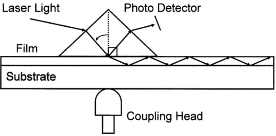
Prism coupling is a useful technique for characterizing the optical properties of light guiding films.21, 22 Prism coupling introduces light into a waveguide through the top surface as shown in Figure 2-2.
Laser Light
Photo Detector
Film
Substrate
Coupling Head
Figure 2-2: Schematic of the prism coupling technique for measuring optical properties of light guiding films.
Light couples into a waveguiding material at incident angles such that the phase of a plane wave in the film is exactly reproduced each time the light reflects .off the bottom interface of the film and then off the top interface. Any destructive interference quickly quenches light propagation. Constructive interference happens at the conditions prescribed by Equation 2-1. For constructive interference to occur, the total change in the phase of a plane wave after two passes through the film and a reflection at each of the interfaces must equal 2m7r where m = 1, 2, 3,..., is the order of the mode. W is the thickness of the film, n is the refractive index, and Film is the incident angle of light inside the film, which can be found based on the angle of light internal to the prism. The reflections at the top and bottom cladding are described by -20Air and
-20Substrate, which are Goos-Haenchen shifts according to Born and Wolf.23
Given the refractive index and thickness of a film and the wavelength of coupled light, (2-1 can be used to predict the number of modes that should be supported by the light guiding medium.
Varying thicknesses of organosilicon polymeric films can be grown using PECVD and thus waveguides with a range of dimensions can be patterned using existing techniques. In this paper, the tunability of the refractive index of organosilicons is demonstrated for the conversion
of a waveguide film from multi mode to single mode across a broad range of wavelengths. This demonstrates high versatility of PECVD organosilicon polymeric light-guiding films for use as a microphotonics interconnect layer.
2.2 EXPERIMENT
Film depositions were carried out in a custom-built vacuum chamber that has been described elsewhere.2 4' 25
Quartz slides and silicon wafers were used for substrates. The chamber pressure was controlled by a butterfly valve connected to an MKS model 252-A exhaust valve controller and was maintained at approximately 300 mTorr. A 13.56 MHz rf source and attached matching network provided capacitively coupled plasma excitation. A shower head used for even inlet gas distribution acted as the powered upper electrode and the substrate stage doubled as the grounded lower electrode. The continuous plasma power was held constant at 50 W. The deposition time was 25 minutes or longer to achieve films that were over 1 pIm thick. For best deposition rate and film uniformity, the stage temperature was maintained at about 50°C.
Hexamethyldisilane (Gelest), 6M2S, was used as the organosilicon precursor without further purification. The monomer vaporized at room temperature and was introduced into the reactor through the shower head assembly. A flow rate near 10 sccm was maintained with a needle valve. The reactor and monomer vessel were purged of air to minimize residual oxygen by pumping the chamber down to 60 mTorr and then filling the chamber nearly to atmospheric
pressure with dry nitrogen (BOC, 99.999%). This cycle was performed at least 5 times before each deposition.
Films deposited using dimethysilane (Gelest), 2MS, as the organosilicon precursor were used to collect some of the initial contrast curves in this study. The deposition conditions for the plasma polymerized 2MS films were the same as those described above. The flow rate of the monomer gas was regulated at 10 sccm using a mass-flow controller.
Contrast curves were collected by irradiating the organosilicon films with varying intensities of UV light and measuring the effect of the light on the material using variable angle spectroscopic ellipsometry (VASE). Plasma polymerized 2MS films were irradiated with 193 nm light using an ArF laser at MIT Lincoln Laboratories. The laser has a spot size of 4 mm and delivers 50 pulses of light per second. An individual pulse has a fluence of 1 mJ/cm2. A dry nitrogen purge stream between the laser and the sample is used to avoid absorption of the radiation by air. Low-energy contrast curves were obtained for plasma polymerized 6M2S films using a 350 W Hg arc lamp obtained from Spectra-Physics. The total power density incident on the sample is 0.5 mW/cm2 as measured using an Orion PD handheld power meter manufactured by Ophir Optronics. Ellipsometry was performed using a J.A. Woolam M-2000 spectroscopic ellipsometer, employing a xenon light source. Data were acquired at three angles (65°, 70°, and 75°) and 225 wavelengths. The Cauchy-Urbach model was used to fit the resulting data yielding film thickness and the film refractive index at 633 nm.
Top-side prism coupling experiments were conducted using a Model 2010 Prism Coupler supplied by Metricon Corporation. The prism coupler uses 633 nm and 1550 nm light sources.
2.3 RESULTS AND DISCUSSION
2.3.1 UV IRRADIATION OF PECVD ORGANOSILICON FILMS
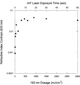
The contrast curve for a PECVD grown film from 2MS in response to 193 nm irradiation is shown in Figure 2-3. 0.1 E CO C, o x -, Q) .t5 coC.,5, 0.01 0.001
ArF Laser Exposure Time (sec)
0 10 20 30 40 50 60
Figure 2-3: Contrast cur
193 nm light. A maximu dosage of 900 mJ/cm2.
0 500 1000 1500 2000 2500 3000
193 nm Dosage (mJ/cm2)
ve for a plasma polymerized dimethylsilane film irradiated with
m refractive index contrast of 0.05 or 3% was achieved with a
At a fairly modest dosage of 900 mJ/cm2, a maximum refractive index contrast of more than 3% was seen as the refractive index dropped by about 0.05 from an initial value of 1.51 measured at 633 nm. Ellipsometry determined that the irradiated film was uniformly oxidized throughout its depth of about 1250 A at low exposure dosages of 300 mJ/cm2and above. To test for preferential oxidation at the surface, the film was modeled in VASE as two distinct Cauchy layers. The refractive index of the bottom layer was assigned the original refractive index of
I I
-I I
1.51. The thicknesses of the two layers and the refractive index of the top layer were varied to
achieve the best fit between the model and VASE data. In most cases, the combined thickness of the two layers were within 1% of the total film thickness and for samples irradiated with more than 300 mJ/cm2 of 193nm light, a thickness of 0 A for the bottom layer resulted in the best fit. As organosilicon polymeric films are oxidized, they begin to resemble polysiloxane materials and become increasingly transparent to the incoming UV radiation. Therefore, underlying material is exposed as the film bleaches and the refractive index of the film becomes even throughout. VASE also verified that the film thickness remained constant with exposure to UV light. Even though oxidation decreases the molecular density, the cross-linked morphology of the plasma polymerized organosilicon film prevents expansion from occurring.
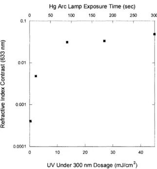
For a much more gradual and controllable decrease in the refractive index, a Hg arc lamp is a better irradiation tool as compared to the ArF laser. Its power flux of UV light under 300 nm is about 2 orders of magnitude less than the 193 nm laser. A Hg arc lamp is more feasible for implementation in a production setting and large surfaces can be evenly irradiated without stepping. Figure 2-4 shows a contrast curve for plasma polymerized 6M2S irradiated with a Hg Arc lamp.