Circuits for Efficient and Secure Power Delivery in
Distributed Applications
MAby
Nachiket Venkappayya Desai
B.Tech., Indian Institute of Technology, Kharagpur (2010)
S.M., Massachusetts Institute of Technology (2012)
SSACUSETS INSTITUTE
OF TECHNOLOGY
MAR
13 2017
LIBRARIES
ARCHNES
Submitted to the Department of Electrical Engineering and Computer
Science
in partial fulfillment of the requirements for the degree of
Doctor of Philosophy
at the
MASSACHUSETTS INSTITUTE OF TECHNOLOGY
February 2017
@
Massachusetts Institute of Technology 2017. All rights reserved.
Signature redacted
A u th o r ... - -- - - -- - -- - ...
Department of Electrical Engineering and Computer Science
November 8, 2016
Certified by...
Signature redacted
Anantha P. Chandrakasan
Vannevar Bush Professor of Electrical Engineering and Computer
Science
Accepted by ...
h
Thesis Supervisor
Signature redacted,z
/Lesl&'.& Kolodziej ski
Chair, Department Committee on Graduate Students
Circuits for Efficient and Secure Power Delivery in
Distributed Applications
by
Nachiket Venkappayya Desai
Submitted to the Department of Electrical Engineering and Computer Science on November 8, 2016, in partial fulfillment of the
requirements for the degree of Doctor of Philosophy
Abstract
The growing number of widely distributed IoT devices presents new challenges in power delivery. Existing frameworks for charging electronic devices, be they wired or wireless, either end up limiting the amount devices can be shrunk due to the size of standardized connectors or end up restricting their free placement due to their reliance on charging mats. The large amounts of vital data IoT devices gather and their heavily distributed nature also makes it important to protect them against unauthorized or malicious charging that might be aimed at damaging and/or stealing data from them. This thesis focuses on developing circuits and architectures to enable a more distributed and secure approach to charging such devices by exploring two topics in particular - energy harvesting and wireless charging.
First, a converter for harvesting power from thermoelectric generators (TEGs) is presented. The converter is capable of cold-starting from a bipolar supply as low as 40 mV, making it suitable for applications where the direction of heat flow from which energy is harvested could be bi-directional. Upon cold-starting from such low voltages, the converter transitions to a high-efficiency mode in steady state that achieves up to 60% efficiency while delivering 110 pW of power. With the goal of building a fully integrated transformer in the future, techniques for modeling an integrated transformer for optimal harvester performance have also been presented.
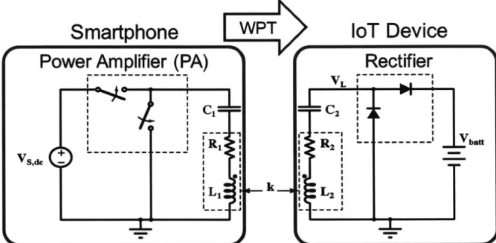
Second, a receiver for device-to-device wireless charging is presented. The receiver dynamically measures the end-to-end system efficiency adjusts the ac input impedance it presents to the wireless power transmission system in order to track the maximum efficiency point. It also employs an inverter-inspired resonant rectifier that overall results in a 13.8% total energy saving for the transmitter with when the received power is 650 mW.
Next, an adaptive rectifier control scheme for wireless power transfer that inte-grates linear regulation into the high-side switches of the rectifier is presented. This has the capability to reduce the area of an integrated converter by eliminating an additional LDO at the output of the rectifier. Additionally, the regulation technique presented results in lower system efficiency degradation when the output power is
regulated below the maximum value.
Finally, a wireless power receiver detuning technique is presented. Detuning al-lows the receiver to protect itself from harmful transients imposed by counterfeit or malicious chargers, by reducing the received power by up to 16 x. It also allows mul-tiple receivers coupled to the same charger to co-operate in order to balance their received powers. Using this technique, the asymmetry in the output powers of two receivers at 4:1 distance ratios from the transmitter can be reversed.
Thesis Supervisor: Anantha P. Chandrakasan
Acknowledgments
It only feels like yesterday when I first set foot on the MIT campus, getting lost multiple times while going from one Orientation event to the next, and feeling like grad school was one big party. While that certainly (and fortunately, I might add) did not turn out to be true, it would be fair to say that this has been the most exciting period of my life and would probably continue to be so. This is a token of my appreciation to everyone that has made these past six years such an amazing journey.
The person I am indebted to the most for making my experience at MIT such a rewarding one would be my advisor, Prof. Anantha Chandrakasan. Not only has he been a constant source of inspiration and support to try out new ideas and push the boundaries of research, but I have learnt so much more from him about topics that might, at first glance, be considered peripheral to academic life, but play a very important role in it - things such as logistics, funding and presenting your work effectively. His propensity for seeking out new ways to solve problems or new ways to improve things by drawing on ideas from a very diverse set of topics, both in research and as part of his administrative responsibilities, continues to baffle me. I can only hope that I am nearly as creative and productive as he is! It has been a great honor and privilege to be his student.
I would also like to thank Prof. David Perreault and Prof. Jeffrey Lang for
being part of my thesis committee. They have been very supportive throughout the entire process and have been extremely accommodative with their schedules, both in scheduling committee meetings and the thesis defense. Their inputs have helped refine this thesis. I have also been fortunate to have learnt a great deal from both of them even before they became part of my thesis committee, through some incredibly well-taught classes on Power Electronics and Electromagnetics.
None of this would have been possible without the financial support that was provided by Foxconn and the MIT Lincoln Labs. I am indebted in particular to Yihui
Qiu
from Foxconn and Scott Van Broekhoven from Lincoln Labs for the confidence they placed in us as well as for their inputs during the course of the work.I have been privileged to have collaborated with some very talented researchers over these years. I learnt a great deal about circuit design and implementing those on silicon from Jerald Yoo, who mentored me during my first two years as a Masters student. More recently, working with Chiraag Juvekar has been an amazing experi-ence, both in terms of learning so much about the theoretical aspects of cryptography as well as spending long days and nights in the lab getting our demo to work. The weekly meetings on the integrated thermal energy harvesting project have been a great learning experience as well, for which I am thankful to Preetinder Garcha, Dina El-Damak, Minjie Chen, Mohammad Araghchini, Jorge Troncoso and Prof. Jeffrey Lang from MIT, and Dennis Buss, Terry Sculley and Joyce Mullenix from Texas In-struments. The extensive discussions with Ujwal Radhakrishna on vibration energy harvesting have also been very enlightening.
provided by TSMC. I am especially thankful to Michael McIlrath at MIT and Arun Achyuthan at TSMC for the fantastic work they do in making sure the process runs smoothly. Chip tapeouts inevitably run late, and I can only imagine how stressful it must for someone to who, on a regular basis, has to make sure all the designs come in on time so that they can be put together and sent to the fab.
I am grateful to Texas Instruments for giving me the opportunity to spend two summers with them as an intern and include the work I did there in this thesis, and to Dennis Buss for his assistance in setting them up. These internships were an invaluable learning experience on how research and development is done in industry and on how projects are conceptualized and evaluated. I would like to thank Yogesh Ramadass and Gianpaolo Lisi for being such great mentors, making sure I was given challenging problems to work on and helping get so much work done in such little time. It was also a pleasure to work closely with Sakshi Arora, Raj Subramonian and Gerard Socci during my second internship.
A large fraction of my time at MIT was spent in the lab, along with other
mem-bers of Ananthagroup. The atmosphere of friendship and cooperation that Anantha has fostered and that previous students have cultivated in this group make it an ab-solute pleasure to be a part of it. Owing to the breadth of the research done in the group, every whiteboard discussion (that usually lasts hours!) is an amazing learning experience. I have learnt so much about RF circuits from Arun and Phil, security from Chiraag and video coding from Mehul and Rahul - topics that I would probably know very little of otherwise. Saurav was an invaluable resource on different aspects of power converter design in the early years. Aside from work, the social aspect of the group is what makes it feel like a second family. I will particularly miss the (almost) daily group lunch in the lab, the procrastination circles and the various Anantha-group sports clubs. I wish the next generation of AnanthaAnantha-group students the best, and hope they keep the culture going.
Margaret, our lab admin, is simply fantastic with all the administrative stuff! It goes without saying that 38-107 functions so smoothly largely due to her diligence in managing accounts and reimbursements, setting up meetings, etc. I would also like to thank the EECS and MTL staff, particularly Janet, Alicia and Debb, for being really supportive over the years. And a special shout-out to the 6.002 Spring 2016 staff and students for making my TA experience so enjoyable.
Outside of work, I have been blessed to have an amazing group of friends. I am especially thankful to my girlfriend, Tanaya, who has been a constant source of love and support. The various culinary endeavors undertaken with my roommates, Sagar and Arun (who did most of the work), will be sorely missed. So will the various weekend hikes, skiing trips with Sivaraman and Vishnu and general hangout sessions with Atulya, Chiraag, Harshad, Mehul, Sai, Sameer, Sayalee, Tapovan, Ujwal, and others. My experiences with taking up Squash and long-distance running during my time here were a lot of fun because of the company of some great folks. It has also been a pleasure being a part of AID-MIT and seeing it grow so much in such little time, in no part due to the tireless efforts of some very dedicated volunteers. I hope it continues to grow in the future.
parents, for their love, support and encouragement to follow my dreams. Throughout my life, they have done their best to make sure I never lacked for anything and have made countless sacrifices in the process. This thesis is dedicated to them.
Contents
Acknowledgements List of Figures List of Tables 1 Introduction 1.1 M otivation . . . . 1.2 Thesis Scope and Organization . . . .2 Ultra-low Startup Thermoelectric Energy Harvesting
2.1 Background . . . . 2.2 Ultra-Low Voltage Startup . . . . 2.2.1 Unipolar Operation . . . . 2.2.2 Bipolar Operation . . . . 2.3 High-Efficiency Steady-State Operation . . . . 2.3.1 Transformer Flux Commutation . . . .
2.3.2 Intermediate Crude Flyback Converter 2.4 Converter Startup and State Transitions . . . 2.4.1 Transformer Multiplexing . . . . 2.4.2 Startup State Transitions . . . . 2.5 Automatic Shutdown . . . . 2.6 Simulation Results . . . . 2.7 Conclusions . . . . 7 15 21 23 23 26 29 . . . 29 . . . 32 . . . 33 . . . 34 . . . 36 . . . 37 . . . 39 . . . 40 . . . 40 . . . 41 . . . 42 . . . 43 . . . 46
3 Integrated Transformer Modeling for Thermoelectric Energy Har-vesting
3.1 Background ... ...
3.2 Existing Integrated Magnetics Solutions . . . .
3.3 Transformer Design Constraints ...
3.3.1 Loop Gain Calculation . . . . 3.4 Transformer Simulation Methodology . . . . 3.4.1 Simulation Runtime Optimization . . . .
3.5 Simulation Results . . . .
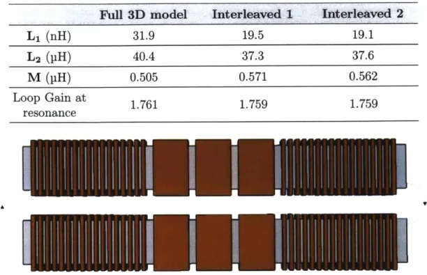
3.5.1 Interleaved Windings . . . .
3.5.2 Toroidal Core . . . .
3.5.3 Changing Core & Wire Widths . . . . 3.5.4 Changing Np and N . . . ..
3.6 C onclusion . . . .
4 Efficiency Maximization for Device-to-Device Wireless 4.1 Background . . . .
4.2 Wireless Power Transmission (WPT) System Model .
4.2.1 Output Power & Efficiency vs. Load . . . . 4.3 Optimal Operating-Point Tracking (OOPT) . . . . 4.3.1 T heory . . . . 4.3.2 Implementation . . . . 4.4 WPT Receiver Design . . ... . . . . 4.4.1 Rectifier Topology Selection . . . . 4.4.2 Integrated Class-cD2 Receiver . . . .
4.4.3 Synchronous Full-Bridge Receiver . . . . 4.4.4 Current-Sense Circuitry . . . . 4.5 Measurement Results . . . . 4.5.1 Test Setup . . . . Charging 4.5.2 Receiver Characterization 49 49 50 51 54 55 56 58 58 59 60 61 63 65 65 67 68 74 74 78 79 79 81 83 84 87 87 . . . . 89
4.5.3 Efficiency and Power Measurements with Transmitter . . . . . 89
4.5.4 System-Level Results . . . . 92
4.6 Conclusion . . . . 99
5 Adaptive Rectifier Characterization and Design for Wireless Power Transfer 5.1 Background . . . . 5.2 Adaptive Rectification . . . . 5.3 Rectifier Modeling . . . . 5.4 Simulation Results . . . . 5.5 Adaptive Rectifier Control for In-band Communication 5.6 Conclusion . . . . 101 . . . . 101 . . . . 102 . . . . 104 . . . . 107 . . . . 110 .. .... 111
6 Wireless Power Receiver Detuning for Authentication and Dynamic Power Allocation
6.1 Background . . . .
6.2 Commonly Used Detuning Techniques . . . . 6.2.1 Switched Passive Component Arrays
6.2.2 Adaptive Duty Cycle Rectifier Control
6.3 Dual-Coil Resonant Frequency Modulation for 6.4 System Architecture . . . . 6.5 Receiver Implementation . . . .
6.5.1 Current Sense-based Rectifier Control .
6.6 Measurement Results . . . . 6.6.1 Test Setup . . . .
Receiver Detuning
6.6.2 Power Blocking and Charger Authentication . . . .
6.6.3 Dynamic Power Balancing . . . .
6.7 Conclusion . . . .
7 Conclusions and Future Work
7.1 Thesis Contributions . . . . 113 113 115 115 116 117 122 124 125 131 131 134 136 138 139 139
7.2 Thesis Summary . . . . 7.3 Future W ork . . . .
A Reactive Impedance Tuning for Maximum Power and Efficiency A. 1 Tuning for Maximum Efficiency-Point Tracking (MEPT) ...
A.2 Tuning for Maximum Power-Point Tracking (MPPT) ...
B Frequency Selection for Near-Field Wireless Power Transmission
C List of Abbreviations Bibliography 140 142 145 146 148 151 155 159
List of Figures
1-1 Some examples of IoT devices and the environments they operate in . 24
2-1 Mechanism of thermocouple operation through the Seebeck effect . 30
2-2 Thermoelectric Generator (TEG) formed by connecting multiple ther-m ocouples . . . . 30 2-3 Examples of TEG and heat sinks . . . . 31
2-4 Schematic of Meissner oscillator . . . . 34
2-5 Schematic of modified Meissner oscillator for bipolar operation . . . . 35 2-6 Schematic of unoptimized flyback converter . . . . 38 2-7 Waveforms for flux commutation in transformer core for positive supply
voltage . . . . 39 2-8 Complete schematic of converter with bipolar Meissner oscillator on
the bottom and dual flyback stages on the top . . . . 40
2-9 Block diagram of complete thermoelectric energy harvesting system . 41 2-10 State transition diagram of converter during startup . . . . 42 2-11 Schematic of circuit used to store maximum value of voltage on anode
of diode D I . . . . 42 2-12 Simulated transient waveforms for startup with 1:100 transformer and
bipolar harvester output voltages at nominal process corner and 2TC 44
2-13 Simulated flyback converter efficiency plots for different input voltages
for N = 100 transformer and a TEG with 5 fl output resistance, at 70% input regulation and with different VSTOR values . . . . 45
3-1 Commonly used inductor geometries . . . . 50
3-2 Flux-gate inductor with magnetic core and copper winding around it 52 3-3 Example of a B-H curve for an anisotropic material . . . . 53
3-4 Top view of integrated flux-gate transformer . . . . 55
3-5 Cross-section of transformer along a vertical plane used for 2D simulation 57 3-6 An example of an interleaved flux-gate transformer . . . . 58
3-7 An example of a toroidal core flux-gate transformer . . . . 59
3-8 Log-log plot of L, and M with varying N . . . . . 62
3-9 Log-log plot of L, and M with varying Np . . . . 63
4-1 Some wearable fitness trackers and their wired charging cables/interfaces 66 4-2 Schematic of two-coil near-field coupling-based WPT system . . . . . 67
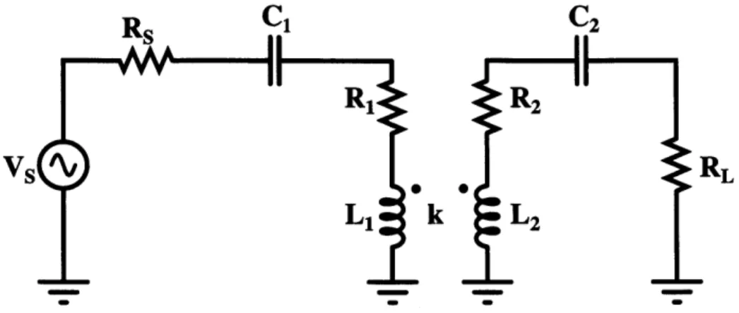
4-3 Schematic of a coupled-inductor WPT system with two coils . . . . . 68
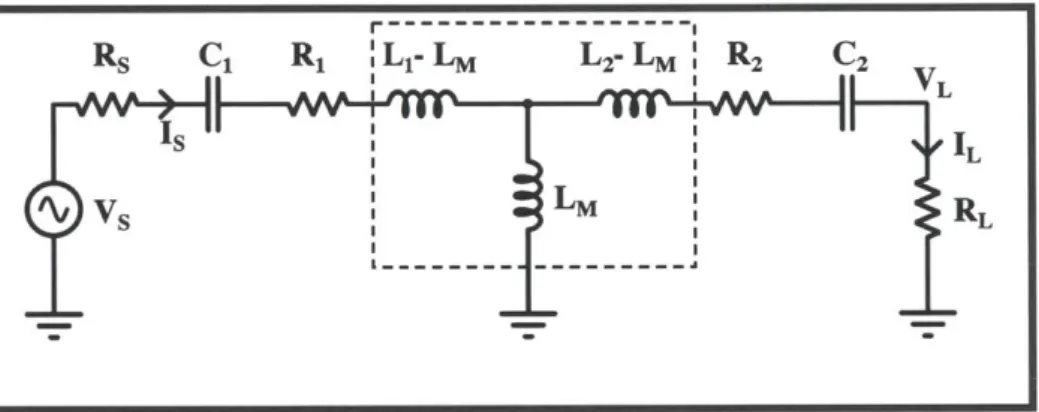
4-4 Simplified circuit model of WPT system . . . . 69
4-5 Output power and power transfer efficiency vs load resistance for WPT system . . . . 71
4-6 Theoretical plot of efficiency vs. load resistance for different values of the coupling factor between two coils . . . . 72
4-7 Theoretical plot of output power vs. load resistance for different values of the coupling factor . . . . 73
4-8 Measured plots of transmit and receive coil inductances . . . . 75
4-9 Pictures of transmit and receive coils used . . . . 76
4-10 Schematic of a coupled-inductor WPT system with coupled inductors replaced by a T-model . . . . 76
4-11 Simulation plot of efficiency and calculated metric vs. load resistance for k = 0.05 . . . . 78
4-12 Block diagram of receiver with boost regulator to control ac input resistance of rectifier RL . . . . 79
4-13 Class-02 rectifier implementation with a diode . . . . 81
4-15 Simulated plot of Z2 . . . . . . . 82
4-16 Block diagram of the Class-02 receiver . . . . 82
4-17 Block diagram of the Synchronous Full-Bridge receiver . . . . 84
4-18 Schematic of current-sense block . . . . 85
4-19 Schematic of comparator-based peak detector . . . . 86
4-20 Measured plot of current-sense + peak detector circuits . . . . 86
4-21 Die micrographs of Class-02 and synchronous full-bridge receivers . . 88
4-22 Photograph of measurement setup . . . . 88
4-23 Rectifier characterization with varying rectifier output voltage (Vrect) 90 4-24 Class-02 receiver efficiency vs. Vbatt for different values of Vrect . . . . 91
4-25 Class-02 Receiver Loss and Control Power Breakup . . . . 91
4-26 Drain and boost (Vd and Vbet) waveforms for the Class-02 receiver . . 93
4-27 Measured link efficiency and computed efficiency metric for Class-02 receiver at k = 0.04 . . . . 93
4-28 Measured link efficiency and calculated metric vs. Vrect at k = 0.07 . 94 4-29 Measured output power and computed metric vs. Vrect for both receivers 95 4-30 Maximum Efficiency-Point (MEP) tracking accuracy for different op-erating conditions . . . . 96
4-31 MEP tracking loop operation as the coupling factor changes . . . . . 96
4-32 Maximum attainable efficiency vs. Vbatt . . . . 98
4-33 Transmitter energy savings with MEPT calibrated to the state-of-charge curve of a standard Li-ion battery . . . . 98
4-34 Charging time penalty with MEPT calibrated to the state-of-charge curve of a standard Li-ion battery . . . . 99
5-1 Inductor current waveform showing short-circuit and power-delivery regions of the cycle . . . . 103
5-2 Inductor current waveform showing symmetric short-circuit and power-delivery regions of the cycle . . . . 104
5-3 Rectifier input voltage waveforms for asymmetric and symmetric
switch-ing cases . . . . 5-4 Plot of input impedance vs.
/
for symmetric switching with p = 0.5using the model derived in Equation (5.3) . . . . 5-5 Magnitude of input impedance of rectifier vs. . . . . 5-6 Phase of input impedance of rectifier vs.
/
. . . . 5-7 Transmitter input power and receiver output power vs. 3 (k = 0.06) . 5-8 Power transfer efficiency vs.#
(k = 0.06) . . . . 5-9 Resistance seen by transmitter Power Amplifier (PA) as/
is varied for the asymmetric switching case . . . .5-10 Phase of transmit coil current with respect to transmitter output
volt-age for the asymmetric switching case (k = 0.06) . . . .
Schematic of two-coil coupled WPT system . . . . Feedback block diagram of the circuit in Figure 6-1 . . . . . Root locus plot for system in Figure 6-2 . . . . Bode plot for system in Figure 6-2 . . . . Receiver with two coils in order to implement detuning . . .
Resonant frequency modulation as auxiliary load resistance is System architecture of receiver detuning-based WPT system Schematic of receiver with two coils for detuning . . . . Basic building block of the main and auxiliary rectifiers . . .
Block diagram of receiver with detuning mechanism . . . . . Current sense-based rectifier control . . . .
. . . . . 117 .118 . . . . . 119 . . . . . 119 . . . . . 120 changed 122 . . . . . 123 . . . . . 124 . . . . . 126 . . . . . 126 . . . . . 127 6-12 Different phases of the operation of current-sense-based duty-cycled
rectifier control . . . .
6-13 Auxiliary rectifier with body diodes highlighted . . . .
6-14 Degree of detuning and blocking vs. effective turns ratio between main and auxiliary coils . . . .
6-15 Picture of main and auxiliary coils on the receiver . . . . 105 106 108 108 109 109 110 112 6-1 6-2 6-3 6-4 6-5 6-6 6-7 6-8 6-9 6-10 6-11 128 129 129 130
6-16 Simulated values of main and auxiliary coil inductances . . . . 131 6-17 Frequency response of receiver to auxiliary rectifier-based detuning . . 132 6-18 Die micrograph of implemented receiver . . . . 133 6-19 Measurement setup for charger authentication and power balancing . 133 6-20 Power regulation with and without detuning . . . . 134
6-21 Receiver visibility at charger . . . . 135 6-22 Authentication flowchart and transmitter and receiver traces during
authentication . . . . 136 6-23 Co-operative power sharing by receivers at different distances from the
charger . . . . 137
6-24 Range of power ratios obtainable by co-operative action by the receivers137
A-i Equivalent circuit model for air-coupled two-coil system . . . . 146
A-2 Plot of efficiency vs. log(RL) and XR . . . . 147
A-3 2D Plot of efficiency vs. XR for RL,n,.m = 0-1 . . . . . . . . . 148 A-4 Equivalent circuit model for air-coupled two-coil system with Theveninized
portion highlighted . . . . 148
A-5 Plot of output power vs. log(RL) and XR . . . . 150 A-6 2D Plot of output power vs. XR for RL,n,.m = 0.1 . . . . 150
List of Tables
2.1 Energy harvesting transformer parasitics . . . . 38 2.2 Comparison with state-of-the-art thermoelectric energy harvesters . . 47
3.1 Errors in simulated transformer inductance parameters vs. values pro-vided by TI . . . . 57 3.2 Effect of interleaving on transformer parameters and loop gain . . . . 59 3.3 Toroidal core transformer parameters and loop gain . . . . 60
3.4 Effect of changing core widths on transformer parameters and loop gain 60
3.5 Effect of changing secondary wire widths on transformer parameters
and loop gain . . . . 61
4.1 Comparison of the Class-cD2 and the synchronous full-bridge receiver
Chapter 1
Introduction
1.1
Motivation
The unprecedented pace at which the semiconductor industry has advanced over the past few decades [1] has revolutionized the way people live all across the world. These advancements have been brought by developments in process scaling [2] and low-power circuit design [3]. Today, the amount of computing power in a handheld smartphone far outstrips that of a large mainframe that took up an entire room fifty years ago, delivered at a tiny fraction of the power and cost. This revolution in the personal electronics space has pervaded every aspect of our lives, affecting how we work, are entertained and interact with other people.
The next great challenge for the semiconductor industry is to build a smarter world, i.e. collect vast amounts of data from every possible source and used it to diagnose problems before they cause catastrophic failures, improve efficiency and achieve better resource utilization. This calls for new machine learning and artificial intelligence algorithms implemented on remote servers that can infer patterns from extremely large datasets, as well as new devices that can collect information, commu-nicate it to the cloud and act upon the results, forming the Internet of Things (IoT). These devices have been enabled through the consistent lowering of power consump-tion of industrial and biomedical sensors [4-8], and of radios [9, 10] reported in lit-erature. Some examples of these in the commercial space include low-power fitness
Automotive Sensing & Traffic Management Healthcare & Fitness Fitbit Home Internet of Automation Things Microwft Band Jawbone Energy Management
Figure 1-1: Some examples of IoT devices and the environments they operate in
trackers for recording physical activity over multiple days, industrial sensors that can detect and relay information about hazards rapidly, indoor environment monitors that can reduce energy consumption in buildings, etc. A few examples of such devices and the environments they operate in are shown in Figure 1-1.
These IoT devices are frequently meant to be deployed in remote or otherwise hard-to-reach locations. Small batteries (less than 1Wh) are the preferred means of powering them in such cases. Even though the devices are meant to be energy-efficient, prolonged use implies the need for an energy source to replenish the energy stored in the battery at frequent intervals, preferably without interfering with their operation. The expected growth in IoT devices, their potential inaccessibility and the unobtrusiveness required of the power delivery mechanism render traditional charging techniques, such as wired chargers delivering power from an ac grid, impractical.
Harvesting and storing ambient energy from the environment is an attractive op-tion for this applicaop-tion. This energy can be in the form of light, heat or vibraop-tion. Each mode of harvesting comes with its own set of challenges. The amount of en-ergy in ambient light depends heavily on the environment under which the system operates, and can vary by up to 100 x between bright sunlit conditions outdoors and standard indoor lighting conditions [11]. Vibration energy harvesting using
piezo-electric crystals is typically narrowband in nature [12] and must be designed with a specific source in mind, such as a motor running at a fixed speed. Thermal energy harvesting is a good candidate for powering low-power sensors in environments with a reliable temperature gradient of a few Kelvin across a junction, which axe commonly found in industrial and biomedical applications. Thermoelectric Generators (TEGs), however, generate few tens of mV under open-circuit conditions for the 1-2 K tem-perature difference [13] that is common in most scenarios. This makes it necessary to design circuits that are able to start up a converter from such low input voltages
without any other form of usable energy present in the system.
Given these limitations, energy harvesting is not suitable for every application, either because it is not reliable or cannot supply the necessary amounts of power under the constraints imposed by the environment the device is operating under. Wireless charging can be a good candidate for recharging the batteries on these de-vices. Current techniques for wireless charging mostly rely on magnetic near-field induction between two inductors placed in close proximity (- 1-5 in.). In this setup,
the transmitter is usually plugged to the 60 Hz ac mains and takes the form factor of a fixed charging mat placed upon a table. This scenario, however, is not particularly suited for charging IoT devices without affecting their functionality. Instead, what is needed is a portable transmitter like a smartphone that can deliver a quick burst of energy to recharge the small battery on the receiver. Here, instead of maximizing received power, it becomes more necessary to maximize end-to-end efficiency since the transmitter is energy-constrained.
The expected growth in the number of wireless charging-capable IoT devices also raises concerns about their interoperability and security. With the development and adoption of a standard for Wireless Power Transmission (WPT), receivers must also be sufficiently protected against malicious or counterfeit transmitters that might ex-pose the receivers to harmful levels of magnetic field or imex-pose transients with the aim of gathering side-channel information. Since the growth in the number of charg-ers cannot be expected to match the growth in the number of receivcharg-ers, most wireless charging systems must be designed to easily accommodate multiple receivers per
charger. In such scenarios, the power delivered to each receiver must reflect its actual needs rather than being dictated by its placement with respect to other receivers receiving power from the same charger.
1.2
Thesis Scope and Organization
This thesis presents circuit- and system-level designs for improved efficiency, reach and security of the power delivery architecture for IoT devices. The work will focus on energy harvesting- and wireless power transmission-based schemes.
The extremely low voltages generated by TEGs make it difficult to start up CMOS circuits with no other energy present in the system. Chapter 2 describes a converter that can cold start from bipolar input voltages as low as +40 mV and, once it has built up enough energy, can transition to a more efficient conversion mode with the same components. In steady state the converter harvests net positive output power from voltages as low as +30 mV. Chapter 3 takes the same topology further with integrated magnetic structures in order to fully integrate the harvester. Based on Finite Element Method (FEM) simulations, a model for an integrated transformer has been built and optimized for the lowest startup voltage of the converter.
In order to charge IoT devices without affecting their functionality, wireless charg-ing capability needs to be extended to portable transmitters. Maintaining high-efficiency operation is one of the top priorities in such a system. Chapter 4 describes a receiver design that is capable of tracking both the Maximum Efficiency-Point (MEP)
and the Maximum Power-Point (MPP) of the entire system without an explicit com-munication link. Maximum Efficiency-Point Tracking (MEPT) minimizes the energy drawn from a constrained portable transmitter for a given amount of energy received. Based on the system requirements, the receiver can be programmed to track maxi-mum efficiency, maximaxi-mum power or a weighted average of the two. The efficacy of this technique is measured for both a resonant rectifier topology and a synchronous
full-bridge rectifier implemented in the same technology. The receiver can track the maximum efficiency point to within 0.7% and achieve 13.8% transmitter energy
sav-ings in the MEPT mode.
In Chapter 5, an adaptive control technique for a synchronous full-bridge rectifier is presented to include load regulation functionality in the rectifier itself. This can reduce the area of an IC implementation by eliminating the linear regulator that is usually connected to the rectifier output. The proposed control technique also results in better system efficiency when the output power is regulated below its maximum. The same method can also be used for implementing in-band communication with-out sacrificing with-output power the way on-off load modulation systems normally do. Chapter 5 presents mathematical models for the rectifier, system simulation results for different flavors of the control technique and the possible in-band communication schemes.
Finally, a wireless power transmission system for IoT devices also needs to incor-porate security to protect themselves from unauthorized and/or malicious chargers.
Chapter 6 presents a receiver-side detuning technique using the rectifier models devel-oped in Chapter 5. Detuning allows the receiver to safely disconnect itself if it wishes not to receive power because a charger is unauthorized or if it is fully charged. This has been used to build a public key-based authentication solution fully implemented on chip that verifies the charger's credentials before turning itself on. It has also been applied to equalize the received power across multiple receivers with different coupling coefficients to the transmitter. With a 4:1 distance asymmetry between re-ceivers, the detuning technique has been demonstrated the capability to reverse the ratio of power delivered in favor of the farther receiver.
Chapter 2
Ultra-low Startup Thermoelectric
Energy Harvesting
2.1
Background
Energy harvesting has become an attractive option for powering wearable, implantable or otherwise hard-to-reach sensors, either directly or through recharging a battery when the harvester output is available only intermittently. While solar cells have been improving in efficiency leading to their widespread use in grid-level power gen-eration, indoor environments make photovoltaic energy harvesting highly unreliable in terms of the output power delivered [11,14]. Piezoelectric and other vibration energy harvesters are typically narrowband in nature, precluding their use in a wide variety of applications [12,15]. On the other hand, thermal energy harvesting is a viable can-didate owing to the presence of reasonable thermal gradients in industrial settings, or between the human body and the environment. For example, Thermoelectric Gener-ators (TEGs) can be used for powering sensors in remote areas of pipelines, or inside moving parts in an automobile. TEGs that are capable of powering wristwatches and sub-mW radios have also been explored and demonstrated [13,16].
Bulk-mode TEGs typically consist of multiple thermocouples made of a bimetallic junction, such as Bismuth Telluride (BiTe). A thermal gradient across a thermocouple
I
[Mkropelt] Heat SourceP
Seebeck Effect Load [Tellurex]Figure 2-1: Mechanism of thermocouple operation through the Seebeck effect
VT
=SA
RT~VTp
Heat Lim, Nasa Tech Briefs, 2008d Asorbed
Substrate,
OrA Connections
Heat
MetalI Rejected Themeeti Interconnections Legs
Figure 2-2: TEG formed by connecting multiple thermocouples
generates a voltage proportional to the temperature difference, as shown in Figure
2-1. This is known as the Seebeck effect. Each thermocouple generates a few mV per
Kelvin of temperature difference across it. In order to generate a reasonable amount of output power (~ 100 11W), multiple thermocouples need to be connected in parallel
thermally to form a TEG. The thermocouples are electrically connected in serially connected strips to generate a high enough output voltage that can be used to operate a power converter. Multiple such strips can then be connected in parallel. TEGs can be modeled as a Thevenin source with output impedance as low as 2 Q [17]. This is shown in Figure 2-2.
Even so, TEGs typically generate around 50 mV at open-circuit for every 1 K of temperature difference across them [18]. Furthermore, depending on the quality
Figure 2-3: Examples of TEG and heat sinks [20]
of heat-sinking from the cold side of the TEG, the actual temperature difference across it might be lower than the temperature difference between the hot side and the environment. The TEG in [18] has a thermal resistance of 2.37C/W and is
30 mm x 30 mm in size. A heat sink of the same size must be chosen to prevent it
from dominating the system volume. A similar sized heat sink in [19] has a thermal resistance of at least 2.4*C/W. From the equivalent thermal circuit between the TEG and the heat sink, the almost equal values of the thermal resistances of the both mean that the temperature difference across the TEG is almost half of the temperature difference available from which energy is to be harvested. This leads to an almost 50% degradation in the effective Seebeck coefficient, and hence the open circuit voltage.
A few examples of TEG and heat sinks are shown in Figure 2-3.
Harvesting energy using TEGs usually implies working off an output voltage as low as 30 mV in the worst case, when the temperature difference across the device is around 2 K and the converter loads the TEG to approximately 70% of its open-circuit voltage. In addition to the low magnitude, the polarity of the induced voltage depends on the direction of heat flow, which could vary across different applications or within the same application (such as HVAC systems). Step-up converters are hence required to convert the TEG output voltage to levels where CMOS circuits can be powered. Cold-starting these converters, i.e. starting up in the absence of any stored energy, proves to be a significant challenge since most switches have threshold voltages far exceeding the output of the TEG. This problem has been addressed
in the past by techniques such as incorporating a battery [21] or precharging an the output capacitor [22] to operate the switches during startup or by integrating a motion-activated mechanical switch [17] - approaches that can significantly increase the cost and complexity of integration. A low-voltage negative resistance oscillator along with a charge multiplier using native MOSFETs is used for startup in [23]. However, its startup voltage is not low enough to provide cold-start capability with TEGs in typical energy harvesting use cases.
To operate off of such low input voltages, two separate transformer-based oscil-lators are used in [24] for both low-voltage startup and steady-state operation, one each for each polarity of the input. A transformer-based oscillator for startup and a transformer-based boost converter are used in [25], leading to higher efficiency but with the capability only to support a single polarity. Transformers are preferred for starting up at low voltages since they offer a purely passive way to amplify a voltage to a level where it can be used to drive a MOSFET. This MOSFET can then be used to provide the negative resistance (otherwise interpreted as loop gain) that sustains oscillations in the circuit.
The thermoelectric energy harvester described in this chapter uses a transformer-based oscillator for ultra-low voltage startup as well. However, the topology employed uses a single transformer both for starting up and for operating in steady state from a bipolar supply. The transformer-based oscillator design ensures the conditions for oscillation are maintained irrespective of supply polarity. Once enough energy has been built up in the system by the startup circuitry, a hard switched, step-up converter takes over to ensure high efficiency operation in steady state.
2.2
Ultra-Low Voltage Startup
The Meissner oscillator (alternatively known as the Armstrong oscillator) was inde-pendently proposed by Edwin Armstrong in 1922 [26] and by Alexander Meissner in
1931 [27], both in connection to building wireless transmitters and receivers. Even
under-lying principle of operation was similar. Oscillations in a circuit are coupled induc-tively and used to drive an active device that reinforces the original oscillation. The same principle can be used with high turns ratio-transformers to enable oscillations from a very small dc voltage that a TEG might produce. The voltage across the high turns ratio side of the transformer can then be used to drive both an active device that provides the loop gain for oscillation as well as a rectifier to generate a de voltage that is much larger from the dc input voltage. One of the earliest implementations of this is described in [28], and subsequently used in a number of commercial products and academic publications [24,25].
2.2.1 Unipolar Operation
A schematic of the Meissner oscillator is shown in Figure 2-4. Since oscillations in
the zero energy state need to start up from the low
(~
30 mV) supply, a nativeNMOS device with zero or negative threshold voltage is used to obtain reasonable g
(transconductance) without sacrificing voltage gain due to the low output impedance of depletion mode devices. Connecting the secondary to the supply instead of ground also serves to increase the gm and thus the loop gain during startup. A transformer with large (N = 20, 50, 100) turns ratio is used to satisfy the loop gain condition. The phase condition is satisfied by the specific connection of the terminals of the transformer. Neglecting leakage inductances and the small-signal output resistance of the MOSFET, the loop gain of the oscillator is
1
LPO(s) = (-gmsL1) - (-N) - L (2.1)
s2 L2Cg +s R2Cg + 1
where Cg is the total capacitance from the gate of the native MOS transistor to ac ground, which includes the gate-source capacitance of the transistor and the winding capacitance of the transformer secondary coil. L1 and L2 are the inductances
mea-sured looking into the primary and secondary of the transformer respectively and R2
is the winding loss referred to the secondary side of the transformer. The first term in Equation (2.1) is the gain of the common-source amplifier formed by the transistor
V,,, VU
1:N
*
VaqT L, L2Native
CNTNMOS
I
- CFigure 2-4: Schematic of Meissner oscillator
and the primary side of the transformer, the second term captures the transformer turns' ratio and the way the terminals of the transformer are connected, and the third term corresponds to the loading of the transformer secondary by the gate capacitance
C9
-From Equation (2.1), it can be seen that the circuit oscillates at
f
= (27rfL2C.g)
The secondary terminal is coupled to a voltage doubler through a dc-blocking capac-itor. The voltage doubler charges a low capacitance node VINT, since the oscillator cannot supply a large load current while satisfying conditions for oscillation.
2.2.2
Bipolar Operation
The expression for loop gain in Equation (2.1) is valid when the supply voltage is positive. For negative supply voltage the loop gain changes to
L neg )= 1 + gmsL, gsL (-N) - 1 (2.2)
s2L
2C, + sR2Cg + 1
The change in the first term of Equation (2.2) compared to Equation (2.1) results in a reduction in magnitude and inversion of phase of the loop gain, which makes the circuit incapable of oscillation when the supply voltage is negative. An intuitive explanation for this is that the native NMOS acts as a source follower instead of a common source amplifier when the supply voltage is negative. The phase shift
V,, VSUP V,VSUP 1:N --L2 CCINT V C 9 -P - L F SUP ---- ---Native:
NMios
Auxiliary Native Branch NMOSI Depletion: -:PMOS
S L -- ----- ---Figure 2-5: Schematic of modified Meissner oscillator for bipolar operation
encountered upon traversing the loop at the frequency where the loop gain is real is then 7r radians, which causes the oscillation conditions to not be met.
In Figure 2-5, we introduce a circuit that can oscillate with a supply voltage of either polarity. This is done by introducing an auxiliary amplifier/source follower branch to complement the action of the native NMOS. This branch acts as a source follower when the supply voltage is positive and has no effect on the phase of the
loop function at resonance. For negative supply voltages, the auxiliary branch acts
as a common source amnplifier and inverts the phase of the loop gain to satisfy the
oscillation criteria. Instead of using a resistive load on the auxiliary branch, an
appropriately-sized depletion mode PMOS is used so that the branch can be turned off after the startup phase is completed.
With the auxiliary branch, the loop transfer functions change to
Lo,,aux(s) Lpos(s) gm,auxr*'aux (2.3)
1+ gm,auxro,aux
where Lp,,(s) and Leg,(s) are as defined in Equations (2.1) and (2.2), gm,aux is the transconductance of the native MOS transistor in the auxiliary branch and ro,aux is
the small-signal output resistance of the auxiliary branch. The current through the auxiliary branch is scaled down from that through the transformer primary branch to ensure the gmr, product remains the same in magnitude at the resonant frequency. This ensures that the magnitude of the startup voltage remains the same irrespective of the polarity of the supply.
2.3
High-Efficiency Steady-State Operation
Once enough energy has been built up in the system by the startup circuit, the har-vester must transition to using a hard-switched converter for high-efficiency operation. Such converters can be designed using either inductive or capacitive energy storage. From a circuit design standpoint, however, using inductor-based power converters offers a number of advantages. In a nutshell, a power converter operates in a number of phases that repeat periodically. In one or more of the phases, the following opera-tions may be performed: energy is drawn from a source, energy is stored in a storage element and energy is delivered to the load at a different voltage from the source, with a correspondingly different current. Most energy sources in the real world are voltage sources. It is theoretically possible to draw energy from a voltage source and store it in an inductor with 100% efficiency when the resistance of the circuit approaches zero. On the other hand, no matter how small the resistance becomes, half of the energy drawn from a fixed voltage source is always lost when storing energy on a capacitor. The difference between inductive and capacitive storage of energy drawn from a fixed voltage source is what allows inductor-based power converters to achieve
100% efficiency in theory, while their capacitive counterparts are theoretically limited
to below 100% efficiency. For example, switched capacitor converters operating from a fixed voltage source can provide 100% efficiency only under no load (open circuit) conditions. Switched capacitor-based topologies can only provide 100% efficiency at non-zero load if adiabatic charging techniques that require multiple voltage sources
at intermediate levels are used.
Since the circuit already has a transformer that is used for startup in Section 2.2, the same transformer that can be used as the magnetic energy storage element for a boost converter. Instead of using the standard inductor-based topology, a topol-ogy resembling the flyback converter can be used with the transformer as the energy storage element. An unoptimized version of this modified topology is shown in Fig-ure 2-6. A switch connected to the primary side of the transformer stores energy in the transformer core in one phase of the driver clock cycle. The stored energy is transferred to the output in the complementary phase by the secondary. Diodes D1 and D2 conduct when the supply is negative and positive respectively.
The converter operates in Discontinuous Conduction Mode (DCM). During steady-state operation, ultra-low power circuits monitor the output for overvoltage, under-voltage etc. These are similar to the circuits described in [29] and operate at 2 kHz. Instead of using a feedback-based Pulse-Frequency Modulation (PFM) control for Maximum Power-Point Tracking (MPPT), a feedforward control technique has been used. Based on the output resistance of the TEG being used, the on-time of the low-side switch of the flyback converter can be set to achieve the desired input reg-ulation level by fusing the appropriate bits of an on-chip EEPROM for a fixed pulse frequency. The feedforward control technique works reasonably well because the TEG output resistance does not change significantly as its output voltage changes. Also, for a converter operating in DCM, the input resistance is uniquely controlled by the low-side on time, with the pulse period and every circuit component at a fixed value. The feedforward control avoids the need for the high-accuracy comparator operating at high frequency that is needed by feedback controllers using PFM control.
2.3.1
Transformer Flux Commutation
The transformers used for the targeted application [30] have large turns ratios and thus large primary winding capacitances, as shown in Table 2.1. Due to this large parasitic capacitance on the primary, the node V,. in Figure 2-6 cannot rise a diode drop above VSTOR for diode D2 to turn on when the supply is positive. Instead,
D2
V,,P
V,,,
V . *:NDI
CSTORswN
Vsec -. SWFigure 2-6: Schematic of unoptimized flyback converter
Table 2.1: Energy harvesting transformer parasitic capacitance values [30] r Primary Winding Secondary Winding
Capacitance (C,) Capacitance (C,)
1:20 4.05 nF 6 pF
1:50 26.7nF 4.8 pF
1:100 84.4 nF 2.8 pF
when the switch turns off under a positive supply the flux in the transformer core
commutates as a result of the resonance between the primary winding inductance and
its associated parasitic capacitance. Diode D1, being connected to the secondary, can easily conduct once the flux in the core changes directions. This is shown in Figure
2-7. This also prevents the large voltage generated by the transformer on the Vec node
in the case where D2 conducts in Figure 2-6. Since diode D2 in Figure 2-6 is not used for either polarity of the converter input V8s,, it can be dropped from the circuit.
In order to allow for the transformer flux to commutate when V,,, is positive, the flyback converter switch needs to be turned off for sufficient time. Based on the secondary winding inductance values in [30] and the capacitance values in Table 2.1, the worst case oscillation period is 2.8 ps for the 1:100 transformer. To accommodate this minimum off-time, the switching period of the flyback converter is chosen to
sw
2 | | | |V
. | |sup pni STFV
secPo
Tra
wer
nsfer
Figure 2-7: Waveforms for flux commutation in transformer core for positive supply voltage
be 16 ps and the maximum possible on-time is 12 ps. Since the flux commutation requires less than a full oscillation period of the secondary winding inductance and capacitance, this allows sufficient time for flux commutation for every on-time setting.
2.3.2
Intermediate Crude Flyback Converter
The complete schematic of the oscillator is shown in Figure 2-8. If the bipolar Meissner oscillator of Section 2.2 were used to charge the large (~ 5 p.F) output capacitor
CSTOR, it would either cease to oscillate or slow down the startup process considerably
because of its limited current-driving capability. Instead, the oscillator is made to charge up a relatively small capacitor CINT, which is isolated from CSTOR, to around 600 mV. The energy stored in CINT is used to operate a ring oscillator that drives
a small, low-Vth switch that drives the flyback converter and charges the output
capacitor CSTOR. The low-Vth crude-stage switch and normal Vth main switch in
Figure 2-8 can be connected in parallel since flux-commutation ensures that the drain of the switches doesn't rise enough to damage the former. The main low-side switch
f~
SWcrd SW r
(Low VT)
Figure 2-8: Complet bottom and dual flyb
V,,, V, 1:N NMOS IL AuxiTa D1 Wd En2 C-T L---Native a sNMOS Auinary Native Branch NMOS Depletion: -::- EnlPMOS
e schematic of converter with bipolar Meissner oscillator on the ack stages on the top
that operates during steady-state is switched at the output voltage, which can be as high as 5.5 V, and achieves higher efficiency.
2.4
Converter Startup and State Transitions
2.4.1
Transformer Multiplexing
The secondary coil of the transformer in the flyback converter of Figure 2-8 is con-nected to the output through a diode and a pass gate. The pass gate allows the path to CSTOR to be turned off when the bipolar Meissner oscillator is operating. The voltage doubler branch going to CINT goes through a depletion mode PMOS device which is only turned off when the flyback converter is operating. Due to the large voltage swing across the secondary coil during flyback operation, all devices connected
Bipolar Ring Crude Sb-gutr
Meissner Osc- V, Osci 44atorl Boost s euao
CS POR Main Main POR &
(~ 0.6 V) IBoost
HClk
Gen fFigure 2-9: Block diagram of complete thermoelectric energy harvesting system
to the secondary terminal - diode D1, depletion PMOS going to the voltage doubler charging up CINT and the native NMOS input of the auxiliary branch - need to be
capable of tolerating large voltages.
On the primary side, the native NMOS transistor from the bipolar Meissner os-cillator is connected in series to a depletion mode PMOS switch that turns off the branch when the flyback converter commences operation, as shown in Figure 2-8. This branch is connected in parallel to the two switches from the flyback converter on the primary side of the transformer.
2.4.2
Startup State Transitions
A complete block diagram of the converter is shown in Figure 2-9, while the states
transitioned by the converter before reaching steady state are shown in Figure
2-10. During cold-start, the bipolar Meissner oscillator charges CINT- Once VINT
crosses the cold start Power-On Reset (POR) threshold, the flyback converter is operated in the crude-boost mode to charge CSTOR till VINT falls below a hysteretic threshold (between 630 mV and 540 mV at 25*C and nominal corner). The bipolar Meissner oscillator then takes over again to charge CINT back to the POR level. The POR trigger-on threshold varies from 630 mV at 25*C and nominal process corner to
500 mV at 1000C and fast corner. During this period CSTOR holds most of its stored
charge since the main sensing and control circuits driven by VSTOR have not yet been activated.
Once VSTOR exceeds the POR trigger-on level by the threshold voltage of a low-Vth switch, energy can be directly transferred from CSTOR to CINT using a sub-regulator,
Cold Start Crude Boost Charges VSTOR, VINT Main Boost
charges VINT Ring Osc. Dischargei VINT Supplies ILOAD
CS POR Triggers Sub-Regulator Starts Main POR Triggers
VINT = 0.6V VsTOR = 1.8V
Figure 2-10: State transition diagram of converter during startup
Vsup En ... D1 CSTOR 1:N En ~,I~cpRleak
Figure 2-11: Schematic of circuit used to store maximum value of voltage on anode of diode D1; the circuit on the primary side of the transformer is the same as in Figure 2-8
considerably speeding up the startup. Once CSTOR is charged to 1.8 V, the main-POR goes high, the main oscillator and control circuits [29] (operating at 2kHz) are activated, and the main primary side switch is used. Upon reaching steady-state operation the startup circuits are disabled using depletion-mode PMOS gating switches to reduce loss in the converter.
2.5
Automatic Shutdown
The thermoelectric energy harvester's output can drop to arbitrarily low power levels depending on the operating conditions. Below a certain threshold, the net energy stored in the magnetic core of the transformer when the low-side of the flyback
con-verter is on becomes insufficient to charge the parasitics on the high-side and turn on D1 in Figure 2-8. However, the switching losses stay the same irrespective of the
TEG voltage. In this scenario, the net energy harvested is negative and it is beneficial
to shut down the converter till more favorable conditions arise.
To detect this condition, the maximum value of the voltage at the anode of diode
D1 is stored on a capacitor C, with a large shunt resistor Rieak to leak the stored charge
with a large time constant, as shown in Figure 2-11. When the input is large enough to turn DI on and supply net positive energy, the voltage stored on the capacitor C, is a few hundred mV above VSTOR. This voltage is compared against VSTOR using a clocked strong-ARM comparator with 1:2 sized input transistors. This provides enough input offset across PVT variation to prevent a small difference (< 100 mV) between the voltages across C, and CSTOR from making the comparator signal that
the TEG voltage is large enough to supply net positive energy. The output of the comparator is checked at the 2 kHz system clock frequency. When the converter shuts off in the absence of adequate power to harvest, only the control circuits that run on the 2 kHz system clock with 330 nA quiescent current are left on. The converter is turned on for 16 cycles every two seconds to check if net positive energy can be harvested.
2.6
Simulation Results
The converter was designed and simulated in a 0.35 pm high-voltage CMOS process with zero-Vth native NMOS and depletion-mode PMOS transistors. TEGs were mod-eled as a voltage source in series with a source resistance varying from 1 to 5 Q, based on which the on-time of the low-side switch in the flyback converter would be set to achieve near-MPPT condition. The transformer was modeled using measured values for the primary and secondary coil inductance, parasitic series resistance and shunt capacitance, and the inter-coil coupling coefficient.
Simulated waveforms for the converter startup at nominal process corner and 27*C are shown in Figure 2-12 for N=100 and input voltages of 40 mV. The VSTOR node
0.6V OVA
0.6 V -
....
....
0 V 0.6 V-0 3J'L~J
I
V VCS POR
Ring Osc
Output
VINT VSTOR 0 V400Ps
(a) V8, = 40 mV 0.6 V-0 v O.6 V-0v 0.6 V 5 V 0 V- --1I111ftl,
jinj
75 ps
-
-ACS POR
Ring Osc
Output
VINT VSTOR ) (b) Vup = -40 mVFigure 2-12: Simulated transient bipolar harvester output voltages
waveforms for startup with 1:100 transformer and at nominal process corner and 27C


![Figure 3-2: Flux-gate inductor with magnetic core and copper winding around it [20]](https://thumb-eu.123doks.com/thumbv2/123doknet/14310232.495210/52.917.97.734.116.505/figure-flux-gate-inductor-magnetic-core-copper-winding.webp)