Design of Low-voltage, High-bandwidth Radio
Frequency Power Converters
by
Jingying Hu
B.S., Illinois Institute of Technology (2005)
S.M., Massachusetts Institue of Technology (2008)
Submitted to the Department of Electrical Engineering and Computer Science in partial fulfillment of the requirements for the degree of
Doctor
ofPhilosophy
MASSACHUSErTS INSTTUTEOF TECHNOLOGY
at the
j
JUL
0 1 2012
MASSACHUSETTS INSTITUTE OF TECHNOLOGY June 2012
@
Massachusetts Institute of Technology, MMXII. All rights reserved.ACHIVES
Department of Electrical Engineering and Computer Science May 21, 2012 Certified by. Professor, Department V - / / of Electrica Engineering David J. Perreault and Computer Science Thesis Supervisor /\
Accepted by
I
U
a Q/- eslie A. Kolodziejski Chairman, Departmental Committee on Graduate StudentsDesign of Low-voltage, High-bandwidth Radio Frequency Power Converters
by
Jingying Hu
Submitted to the Department of Electrical Engineering and Computer Science
on May 23, 2012, in partial fulfillment of the
requirements for the degree of Doctor of Philosophy
Abstract
T
HE MASS and volume required for power electronics circuitry is a dominant obstacleto the miniaturization and integration of many systems. Likewise, power electronics with greater bandwidth and efficiency are becoming vital in many applications. To realize smaller and highly responsive power electronics at low voltages, this thesis explores devices, circuits, and passives capable of operating efficiently at very high frequencies (VHF, 30-300 MHz). Operation at these frequencies enables reduction of the numerical values and physical size of the passive components that dominate power converters, and enables increased bandwidth and transient performance which is valuable in a multitude of low-voltage and low-power applications.
This thesis explores the scaling of magnetic component size with frequency, and it is shown that substantial miniaturization is possible with increased frequencies even considering material and heat transfer limitations. Moreover, the impact of frequency scaling of power converters on magnetic components is investigated for different design criteria. Quantitative examples of magnetics scaling are provided that clearly demonstrate the benefits and opportunities in VHF magnetics design. It is shown to utilize the advantages of frequency scaling on passive component size that system losses and other limitations must be considered. One such area that is examined is semiconductor device requirements, where through a combination of device layout optimization for cascode structures and integrated gate drive designs on a 0.35-um CMOS process, converter performance (i.e., loss and bandwidth) can be significantly improved in the VHF regime.
In this thesis a dc-dc converter topology is developed that is suitable for low-voltage power conversion and employs synchronous rectification to improve efficiency. The converter is also comprised of a high-bandwidth and high-switching-frequency inverter topology that can dynamically adjust the output power from one-quarter to full power, while maintaining good efficiency. Furthermore, with its inherent capability of gate-width switching, the inverter can further reduce gating loss by one-half resulting in substantial performance improvements at light load operation.
A major contribution of this thesis is the development of a synchronous rectifier operating in the
VHF regime. VHF power conversion is especially challenging at low voltages due to poor efficiency resulting from rectification loss. To overcome diode rectification loss, the benefits of synchronous rectification are discussed in the context of a 100MHz class-E resonant rectifier, which results in a
2.5 x overall converter efficiency improvement. The culmination of the developed design techniques in
passives, semiconductor devices, and circuit topologies is an experimental prototype of a miniaturized
Acknowledgements
I want to thank Prof. David. J. Perreault, my thesis advisor, for his guidance, teaching, patience
and support throughout the course of this journey. I am grateful to have been given the opportunity to work with such an outstanding researcher, educator and mentor. Thank you for helping me grow as a student and as a person.
My thanks go to my thesis committee: Prof. Joel. L. Dawson and Prof. Jeffrey H. Lang for their
advice, knowledge, direction and support along the way. I am very fortunate to have the chance working with and learning from you.
To Anthony and Juan, for generously sharing their insights, expertise and experience throughout the years. Thank you for being there for me through the ups and downs of this entire process. To the past and present members of my research group and LEES, Wei, Justin, Yehui, Alex, Saman-tha, Minjie, Wardah, Seungbum, John, Nate, Robert, Brandon, Jiankang, Warit, Sam and Uzoma for their help, support and company. Thank you for making the past few years a fun learning expe-rience for me. I am also thankful for all the assistance I have received from my colleagues and staff from LEES.
To all my friends that have supported me during my graduate studies, Wenting, Rui, Sahar, Sushma, Wenjia, Maje, Grace, Marcus, Jason, Fred, Courtney, Keith and Melinda for celebrating with me during the happier times and commiserating with me through the tough ones. I am very blessed to have been surrounded by such an incredible group of individuals.
To George, thank you for being there with me during this amazing journey, filling it with laughter, happiness and beautiful memories. Words simply cannot express my gratitude for everything you have done and everything you have been to me. Thank you for making my MIT experience truly incredible and memorable.
I dedicate this thesis to my parents and my grandparents, thank you for teaching me so much about
love, life and work. It is impossible to express how thankful I am to have you in my life. Without your unconditional love and support, I would be nowhere close to where I am today.
1 Introduction
1.1 Challenges of Increasing Converter Switching Frequency . . . . 1.2 Very High Frequency Resonant Power Conversion . . . .
1.3 Contributions and Organization of the Thesis . . . .
2 Magnetics Scaling
2.1 Background . . . . 2.2 Magnetics Scaling Design Considerations . . . .
2.3 Magnetics Scaling Method and Procedure . . . .
2.3.1 Numerical Analysis Procedure . . . .
2.4 Magnetics Scaling Analysis . . . . 2.4.1 Cored Inductor Scaling . . . .
2.4.1.1 Cored Inductor Design Examples . . . 2.4.1.2 Temperature Constraint . . . . 2.4.1.3 RF Low-Permeability Materials . . .
2.4.2 Coreless Inductor Scaling . . . . 2.4.2.1 Coreless Inductor Design Example . . 2.4.3 Magnetics Scaling Summary . . . .
3 Integrated Device and Gate Drive Design
3.1 Background . . . . 3.2 Device Design . . . .
3.2.1 Device Layout Optimization . . . .
3.2.2 Cascoded Structure . . . .
Contents
17 18 20 21 25 . . . . 25 . . . . 27 . . . . 28 . . . . 28 . . . . 29 . . . . 29 . . . . 31 . . . . 34 . . . . 35 . . . . 36 . . . . 39 41 43 . . . . 44 . . . . 45 . . . . 47 . . . . 52Contents
3.3 Integrated Gate Drive Design . . . . 60
4 Parallel/Series Reconfigurable Inverter Design 65 4.1 Background . . . . 65
4.2 Inverter D esign . . . . 67
4.2.1 Inverter Tuning Procedure . . . . 69
4.2.1.1 Design Considerations about CEX1 and CEX2 . . . . . .. 72
4.2.2 Gate Width Switching . . . . 75
4.3 Inverter Implementation and Experimental Results . . . . 77
5 Parallel/Series Reconfigurable Converter Design 83 5.1 B ackground . . . . 84
5.2 Rectifier D esign . . . . 85
5.3 Class-E Synchronous Rectification . . . . 87
5.3.1 Rectifier Tuning Procedure . . . . 89
5.3.2 Converter Tuning . . . . 90
5.4 Converter Implementation and Experimental Results . . . . 95
6 Summary and Conclusions 103 6.1 Thesis summary and key take-aways . . . . 103
6.2 Thesis Conclusions . . . . 105
6.3 Future W ork . . . . 106
A Appendix A 109 A.1 Magnetics Scaling Code . . . . 109
B Appendix B 127 B.1 Inverter Boards and Schematics . . . . 127
Contents
D Appendix B 147
D.1 Converter Boards and Schematics ... 147
D Appendix B 147
D.1 Converter Boards and Schematics ... 147
List of Figures
1.1 Class E Inverter . . . . 20 1.2 Schematic depiction of VHF converter under on-off modulation. . . . . 21
2.1 Cored inductor scaling analysis procedure. Matlab script implementing this procedure is provided in Appendix A. . . . . 30
2.2 Numerical Optimization results of inductor "box" volume vs. design fre-quency for an example resonant inductor . . . . 32 2.3 Core loss and winding loss of an optimized resonant inductor vs. design
frequency for a set of inductors realizing a constant impedance of 62.8 Q (i.e.
100 pH at 100 kHz) at
Q
= 100 for 1 A ac current. Numerical simulationfiles are included in Appendix A. . . . . 33
2.4 Numerical optimization results of inductor "box" volume (including discrete designs) vs. design frequency for a set of inductors realizing a constant impedance of 157 Q (i.e. 250 pH at 100 kHz) at
Q
= 100 for 1 A peakac current. Numerical simulation files are included in Appendix A. . . . . . 33 2.5 Thermal resistance vs. surface area for different data and models . . . . 35 2.6 Numerical Optimization results of inductor "box" volume vs. design
fre-quency for an example resonant inductor with temperature limitations for a set of inductors realizing a constant impedance of 62.8 Q (i.e. 100 pH at 100 kHz) at
Q
= 100 for 1 A ac current. Numerical simulation files are included in A ppendix A . . . . 36 2.7 Resonant inductor volume comparison. The use of the rf material enablesa - 40% reduction in volume as compared to using 3F3 material for this
scaling exam ple. . . . . 37 2.8 Magnetic Dimension Scaling . . . . 37 2.9 Single layer coreless solenoid inductor . . . . 39
2.10 Numerical Optimization results of inductor "box" volume vs. design fre-quency for an air-core resonant inductor with temperature limitations (400C) for a set of inductors realizing a constant impedance of 62.8 Q (i.e. 100 pH at 100 kHz) at
Q
= 100 for 1 A ac current. Numerical simulation files areList of Figures
2.11 Comparison between conventional magnetic material (3F3), RF material (P) and coreless inductor volume for a set of inductors realizing a constant
impedance of 62.8 Q (i.e. 100 [H at 100 kHz) at
Q
= 100 for 1 A ac current.Numerical simulation files are included in Appendix A. . . . . 41
3.1 A single transistor cell. . . . . 46
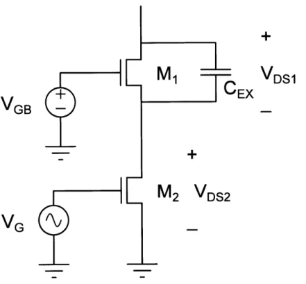
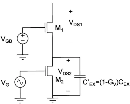
3.3 Device stacking configuration, top device M1 in a common-gate configuration
with its gate connected to a dc bias voltage, and the bottom device M2 in a common-source configuration gated on and off at the switching frequency. . 53
3.4 Unequal voltage sharing in a cascode pair. A 100MHz class-E inverter is designed with a cascoded pair with two identical devices, figure 4.4. Without additional capacitance across M 1, the bottom device absorbs most voltage
stress on the cascode structure, resulting in the total breakdown voltage significantly less than twice of a single device. The component values are:
CF = 150pF, LR = 17nH, CR = 200pF and RL = 2.15Q. Simulation files
are included in Appendix D. . . . . 54 3.5 Additional capacitance across Mi can address issues of unequal voltage
shar-ing and lossy transition state for a cascode device. . . . . 55 3.6 Adding additional capacitance across M1 allows the drain voltage to be
shared more equally between the two devices. A 100MHz class-E inverter is designed with a cascoded pair with two identical devices, figure 4.4. With additional capacitance across M1, the drain voltage is shared equally between
the top and the bottom device. The component values are: CF = 150pF,
CEX1 = 50pF, CEX2 = 120pF, LR = 17nH, CR = 200pF and RL 2.150.
The calculated CEX1 value from Equation 3.5 is 51pF. Simulation files are
included in Appendix D. . . . . 56 3.7 Due to Miller effect, CEX across Mi effectively appears as a negative
capac-itance across M 2. . . . 57
3.9 A tapered buffer gate driver with N-stages and a tapering factor of F. . . . 61 3.10 The normalized delay time to N(C + Cy) through the inverter
chain given the device CIss = 82pF, the output capacitance, and the
in-put capacitance of a single inverter on TSMC035HV process. The optimum number of stages in this case is 7. . . . . 61 3.11 The split capacitor model of a tapered inverter chain [1]. . . . . 62 3.12 Simulated Tapered Inverter Chain Gate Drive Waveforms. The waveforms
shown are the simulated Cadence waveforms for a 7-stage tapered driver with a tapering factor of 4 after stage 1,3,5 and 7. The input capacitance of the
List of Figures
4.1 Class E Inverter Performance vs. Load Resistance . . . . 66
4.3 Series/Parallel Drain and Gate Drive Voltage Waveforms. VGB is the gate bias voltage applied on the common-gate device in the cascode structure M 1, VB is the gate voltage on the common-source device M2 and is switching at the operating frequency 100MHz. The inverter drain voltage VDS across each cascode device and the voltage across the bottom device of the cascode structure are also shown. Relevant simulation files can be found in Appendix B . . . . .. . . .. . . . . 70
4.4 Class E Inverter . . . . 70
5.1 Resonant RF dc-dc Converter Block Diagram. . . . . 84
5.3 Fully-resonant Class E rectifier . . . . 86
5.5 Resonant class-E synchronous rectifier . . . . 88
5.6 A class-E synchronous rectifier and its voltage and current waveforms. At an output voltage of 1V, the component values are: CREC = 100pF, LREC = 23nH, LIN = 5nH, COUT = 0.001pF. Simulation files are included in A ppendix C . . . . . 89
5.7 Synchronous rectifier's input impedance. . . . . 91
5.8 Synchronous rectifier's peak voltage vs. duty ratio. By adjusting CREC and LRE.C, the peak voltage and the length of the conduction interval of the switch can be traded off. Simulation files for this example may be found in the Appendix C. . . . . 92
5.9 Dc-dc converter with synchronous rectifier. The converter may be achieved by connecting the inverter introduced in Chapter 3 with the rectifier topology. 92 5.10 Dc-dc converter with synchronous rectifier and a transformation network. The transformation network components LM and CM may be absorbed into LR and CREC. ... ... 93
5.11 100MHz dc-dc converter with synchronous rectifier simulation waveforms. The operating conditions are VIN = 2.3V, POUT = 1.5W, VOUT = 1V, and fsw = 100MHz. Component values are Ci = C2 =0.0l1pF, LF1 = LF2 = 18.5nH, CEX1 = CEX3 = 47pF, CEX2 = CEX4 = 80pF, C3 = 0.01pF, LR = 10nH, CR = 390pF, CREC = 200pF, and LREC = 12.5nH. Simulation files are included in Appendix C. . . . . 94
5.12 100MHz dc-dc converter with ±1ns of timing variation in the synchronous
rectifier.The operating conditions are VIN = 2.3V, POUT = 1.5W, VOUT =
1V, and fsw = 100MHz. Component values are C1 = C2 = 0.01pF,
LF1 = LF2 = 18.5nH, CEX1 = CEX3 = 47pF, CEX2 = CEX4 = 80pF, C3 =
List of Figures
5.14 Timing adjustment circuitry for the 100MHz dc-dc converter with syn-chronous rectification. A 3.3V ECL programmable delay chip MC100EP195 is used to generate the time delay block TD, which can achieve a time delay between 2.2ns to 12.2nS, with approximately 10ps increments. The detailed
schematics and board layout are included in Appendix C. . . . . 97
5.16 Converter model including all critical layout and packaging parasitic induc-tances. This model is attained via measurements of the PCB board in the impedance domain. With all other component values the same as those in figure 5.11, the additional parasitic component values are: LPAR1 = 0.6nH, LPAR2 = 0.5nH, LPAR3 = lnH, LPAR4 = 1.3nH, and LPAR5 = 0.5nH. The simulation files capturing this model are included in Appendix C. . . . . 98
B. 1 Parallel/Series reconfigurable inverter board -top copper layer . . . . 127
B.2 Parallel/Series reconfigurable inverter board -layer-2 copper . . . . 128
B.3 Parallel/Series reconfigurable inverter board -layer-3 copper . . . . 128
B.4 Parallel/Series reconfigurable inverter board -bottom copper layer . . . . . 129
B.5 Parallel/Series reconfigurable inverter board -schematic . . . . 130
B.6 100MHz Parallel/Series reconfigurable inverter . . . . 131
B.7 100MHz Parallel/Series reconfigurable inverter, effect of C3 . . . . 131
B.8 100MHz Parallel/Series reconfigurable inverter, effect of CEX on equal volt-age sharing . . . . 132
B.9 100MHz Parallel/Series reconfigurable inverter, no additional capacitance across top device in the cascoded structure . . . . 132
B.10 100MHz Parallel/Series reconfigurable inverter, effect of parasitics . . . . . 133
B.11 100MHz Parallel/Series reconfigurable inverter, effect of parasitics part 2 . 134 D. 1 Parallel/Series reconfigurable converter with synchronous rectifier board -top copper layer .. ... ... ... ... .... ... .. . 147
D.2 Parallel/Series reconfigurable converter with synchronous rectifier board -layer-2 copper . . . . 148
D.3 Parallel/Series reconfigurable converter with synchronous rectifier board -layer-3 copper . . . . 149
D.4 Parallel/Series reconfigurable converter with synchronous rectifier board -bottom copper layer . . . . 150
D.5 Parallel/Series reconfigurable inverter board - schematic . . . . 151
List of Figures
D.7 A fully resonant class-E rectifier. . . . . 152 D.8 A fully resonant class-E synchronous rectifier. . . . . 153 D.9 In fully resonant class-E synchronous rectifier, there is a tradeoff between
duty ratio and peak device voltage. . . . . 153 D.10 100MHz Parallel/Series reconfigurable converter with synchronous rectifier. 154
D.11 100MHz Parallel/Series reconfigurable converter with synchronous rectifier.
The rectifier is somewhat insensitive to the time delay of its gate drive voltage. 155
D.12 100MHz Parallel/Series reconfigurable converter with synchronous rectifier
with packaging and layout parasitics.
D.1 Parallel/Series reconfigurable converter with synchronous
top copper layer . . . . D.2 Parallel/Series reconfigurable converter with synchronous
layer-2 copper . . . .
D.3 Parallel/Series reconfigurable converter with synchronous
layer-3 copper . . . .
D.4 Parallel/Series reconfigurable converter with synchronous bottom copper layer . . . .
D.5 Parallel/Series reconfigurable inverter board - schematic .
D.6 Conventional class-E rectifier. . . . . D.7 A fully resonant class-E rectifier. . . . . D.8 A fully resonant class-E synchronous rectifier. . . . . D.9 In fully resonant class-E synchronous rectifier, there is a
duty ratio and peak device voltage. . . . .
rectifier rectifier rectifier rectifier tradeoff board -board board -board -between . . . . 156 147 148 149 150 151 152 152 153 153 D.10 100MHz Parallel/Series reconfigurable converter with synchronous rectifier. 154 D.11 100MHz Parallel/Series reconfigurable converter with synchronous rectifier.
The rectifier is somewhat insensitive to the time delay of its gate drive voltage. 155
D.12 100MHz Parallel/Series reconfigurable converter with synchronous rectifier
List of Tables
3.1 Integrated Device Parameters, Predicted . . . . 52 3.2 Integrated Device Parameters, Measured . . . . 52 4.1 Component Values and Specifications for Parallel-Series Inverter . . . . 79 5.1 Component Values and Specifications for Parallel-Series Converter with
Chapter 1
Introduction
T
HE SIZE of power conversion electronics is a dominantobstacle to achieving further miniaturization and integration of many modern mobile and communication systems. Moreover, power electronics having higher efficiency and control bandwidth are important for reducing the overall energy consumption of communications electronics.
In spite of the need for smaller and better dc-de power converters, it is difficult for many ex-isting conventional power converter designs to provide wide operation range while maintain-ing high efficiency and a small volume. Furthermore, while switched mode power supplies
(SMPS) have taken advantage of scaling trends in the form of improved semiconductors
and higher integration, the bulk energy storage (comprising most of the volume) required at contemporary switching frequencies of a few megahertz and below has not scaled to the same degree, leaving most commercial converters with a not-so-subtle footprint. Shrinking passive component volume at constant numerical component value and energy storage is one obvious way to target the needs for a smaller converter. However, fundamental scaling issues that bring efficiency down beyond acceptable limits make this approach impractical.
An alternative method to resolve the tradeoffs between small size and high efficiency is to reduce the required energy storage and passive component values by increasing the switching frequency [2]. The numerical values and energy storage requirements of energy storage elements (e.g., inductors and capacitors) required to achieve a given conversion function vary inversely with switching frequency (see, e.g., [2, Chapter 6]). Moreover, a higher switching frequency and reduced intermediate energy storage enable faster response to load transients and reduce the size of ancillary filter components (e.g. output capacitors). Higher switching frequencies can considerably widen converter control-loop bandwidth, which is typically limited to about a tenth of the switching frequency.
Introduction
The advantages of increasing switching frequency suggest that this method may hold the key to achieving designs that can meet all the demands of the next generation mobile and communication systems. This, in fact, has been an ongoing pursuit in power electronics since at least the 1970's [3] as switching frequencies have risen from tens of kilohertz to a few megahertz.
To design power converters at radically increased switching frequencies that attain signifi-cant reduction in passive component size requires leveraging semiconductor device technol-ogy, novel circuit topologies, and unconventional system architectures. Such designs also benefit from increased integration of devices (especially including integrated circuit
technol-ogy), improved passive components, and better packaging. This thesis will develop design
techniques for high-performance, low-voltage dc-dc power converters. Design of suitable switching circuits and integrated gate drivers in CMOS technology will be explored, along with improved controls and their application in various circuit topologies and functions. Together, these approaches will address design challenges associated with high-efficiency and high-bandwidth power conversion at low voltages. The new architectures, circuits and controls considered are expected to enable substantial miniaturization and improve response speed of inverters and dc-dc converters, and to permit improved performance in multiple applications.
1.1
Challenges of Increasing Converter Switching Frequency
A typical switched-mode power stage consists of semiconductor devices and passive energy
storage elements. While losses are distributed among the active and passive components in the power stage of a converter, the bulk of the system mainly resides in the volume of the passive elements. Increasing operating frequency can significantly improve the size, cost and transient response of the system. However, increasing power loss at higher operating frequency in conventional converters places an upper bound on the switching frequency. Switching power MOSFETs have experienced tremendous improvements in the last twenty years, yielding devices with lower on-state resistance and smaller packages. However, under high frequency operation, switching loss (including loss associated discharging the out-put capacitance and overlap loss), instead of conduction loss, becomes the dominant loss
1.1 Challenges of Increasing Converter Switching Frequency mechanism in a conventional hard-switched converter. This has imposed a upper limit on acceptable switching frequencies in such converters.
Another loss mechanism closely related to the characteristics of switching devices such as MOSFETs is gating loss, which results from charging and discharging the device input capacitance, CIss. For both lateral and vertical MOSFETs, gating loss has a linear de-pendency on the switching frequency [4, 5]. In the case of a conventional hard-switched
converter, the gating loss is described by the following equation:
PGATE = QGATEVGATEf = CGATEVGATEf (11
For a typical commercial 20V vertical MOSFET having a 2A current rating with effective gate capacitance of 200 pF operating at a switching frequency of a few megahertz, the loss is measured from hundreds of milliwatts to over a watt, which makes the efficiency unacceptable for low-voltage, low-power designs.
In addition to the conduction loss, switching loss and gating loss associated the semiconduc-tor devices, frequency-dependent losses resides in the magnetic components are yet another loss mechanism eating away efficiency. Inductors, incorporating conventional magnetic ma-terials may operate fine at low frequency. However, As the frequency is scaled up, core losses, captured by the Steinmetz equation 1.2, imposes a fundamental operating frequency limit of these materials. For conventional cored inductor, this frequency limit doesn't usually exceed a few megahertz, beyond which magnetics loss increases substantially.
P,(t) = kf"BO (1.2)
Altogether, these major loss mechanisms associated with conventional converter designs suggest that alternative design methods must be exploited to improve converter performance if we are to increase switching frequency to reduce the volume of modern switch mode power supplies.
Introduction
Lchoke LRCR
CP
RL
Figure 1.1: Class E Inverter
1.2
Very High Frequency Resonant Power Conversion
The predicted poor performance of conventional hard-switched converters at high frequency, exacerbated in the case of low-power converters, suggests that resonant power conversion may be a more viable candidate as the switching frequency moves beyond a few megahertz. Efficient power conversion at high frequency has been achieved using switched-mode RF inverters taking advantage of zero-voltage switching (ZVS) [3-19]. Inverters like the Class
E inverter [6-8], Figure 4.4, have been popular in various applications. By utilizing
reac-tive elements to shape the voltage and current waveforms, resonant power conversion can eliminate the significant amount of switching loss faced by traditional hard-switched con-verters at higher operating frequencies. Taking the advantages of resonant network one step further, gating loss can also be significantly reduced when a resonant network recycling a portion of the gate energy each cycle is utilized to drive the gate [4,5,18-24].
However, resonant power conversion has its own challenges, which limits its range of use. Reactive elements in resonant topologies are usually tuned to provide desirable ZVS perfor-mance (and high efficiency) at a single operating point. However, as the load moves away from the nominal load value, with which the resonant topology is tuned, converter perfor-mance can plummet. Furthermore, designing a suitable control method is also a non-trivial issue. Duty ratio control becomes difficult (if not impossible) to implement for resonant converters at high frequencies. Controlling power by varying switching frequency yields varying component stresses and efficiency reductions across load control limitations become yet another drawback for high frequency resonant converters.
1.3 Contributions and Organization of the Thesis
VREF REF COp
ompdrive
~dc-dc
Cconverter CBULK RL
Figure 1.2: Schematic depiction of VHF converter under on-off modulation.
Burst mode control [4,15,18,24,25] has been shown to address the control challenges above,
by separating the control function from the power stage operation of the converter, Figure
1.2. The converter cell is switched on and off at a modulation frequency, often much lower than the converter switching frequency, to control the average power delivered to the output. When the converter is on, it delivers a fixed power maintaining ZVS characteristics and good efficiency. When off, no power is delivered and there is no associated resonating loss. A particular implementation of this on/off control method [26], enables fast transient response and efficient light-load operation while providing controlled spectral characteristics of the input and output waveforms, which makes this control method suitable in a variety of applications (such as communication systems). In addition, a hysteretic override technique may further allow the converter to reject load disturbances with a bandwidth much greater than the modulation frequency, limiting output voltage disturbances to within a fixed value. Such operation allows the network to be tuned to enforce ZVS at one particular operating point. The result is maximum efficiency, better dynamics, and higher achievable operating frequency. The fact that this mode of operation allows much higher switching frequency is self-reinforcing-high frequency means less energy storage so the converter can be started and stopped more rapidly and achieve a wider load range.
1.3
Contributions and Organization of the Thesis
As suggested in the previous discussion, VHF resonant power conversion is a suitable de-sign method for low power converters to meet the two major concerns of future portable
Introduction
sonable Qs in the range of 60-120 operating at VHF regime can completely eliminate the frequency-dependent core losses. For capacitors, VHF operations reduces the total required capacitance value, leading to much smaller volume.
The primary goal of this thesis is to develope designs and techniques suitable for high-bandwidth RF power conversion at low voltages. There are three major areas that this thesis work will focus on: passives, devices, and circuits. The following chapters will address the topics in turn.
Chapter 2 explores magnetics design tradeoffs and scaling in VHF dc-dc converters, and examines how the physical sizes of magnetic components change with increasing frequency for different design options. We provide quantitative examples of magnetics scaling, and also point to opportunities in VHF magnetics design.
Chapter 3 examines methods to improve upon performance achievable via commercial off-the-shelf semiconductors for use in VHF applications. The variety and quality of discrete commercial MOSFETs with breakdown voltages lower than 20 V are very limited. Even the available ones are generally optimized for hard-switched applications. One can thus realize substantial performance improvements by designing customized devices in an integrated
CMOS process. With custom design, one can attain significant reduction in switching,
conduction and gating loss via modifying device layout, device packaging and extending safe operating area (SOA) in a low-voltage CMOS process. However, even when a optimal device geometry (for a given design) has been determined, driving the input capacitance of such a device at tens to hundreds of MHz is not a trivial issue. Integrating gate drivers on the same process introduces even more opportunities to achieve better performance. Through the magnetics scaling analysis, the most desirable range of operating frequencies can be determined. From which, a device geometry can also be reached via the device optimization algorithm along with a low-power gate driver design. Chapter 4 explores various circuit topologies as a means to leverage the optimized device/gate drive design in the tens to hundreds of MHz operating regime. Specifically, a inverter topology operating at hundreds of MHzs that can dynamically adjust the output power from full power to 1/4 of the full power level is introduced. Furthermore, this topology allows for an alternative gating scheme that further cuts down the gating loss by half, which directly translates to substantial performance improvements at light load. This topology operates at fixed
1.3 Contributions and Organization of the Thesis frequency and duty ratio. It eliminates the need for bulk inductors and provides excellent transient response. Compared to its counterparts, this design is specifically optimized to address the unique challenges of high-bandwidth low-voltage low-power designs.
Chapter 5 presents a full dc-dc converter utilizing the inverter topology discussed in Chapter 4. Advantages of synchronous rectification at low voltages is discussed in the context of a 100MHz class-E synchronous rectifier. The culmination of the developed design techniques in passives, semiconductor devices, and circuit topologies is an experimental prototype of a miniaturized 100MHz, 1W power converter utilizing synchronous rectification.
Resonant power conversion at VHF regime has proven its merits in the context of a low-power, low-voltage, high bandwidth dc-dc converter. Chapter 6 summarizes the design considerations for VHF resonant power conversion and suggests direction for continued work in this area.
Chapter 2
Magnetics Scaling
A
S INTRODUCED in Chapter 1, power electronics operatingat very high switching frequency (e.g, 10-100 MHz) are important in many applications including resonant inverters for heating, plasma generation, imaging and communications [6,10, 27-31] and resonant dc-dc converters [7,17,28,32-35]. Magnetic components play an important role in these applications for intermediate energy storage, impedance transformation, and filtering. These magnetic components should have a high quality factor and low loss in order to achieve highly efficient power conversion.
In this chapter, we explore frequency scaling of power converters, and examines how the physical sizes of magnetic components change with increasing frequency for different design options. We provide quantitative examples of magnetics scaling, and also point to opportu-nities in VHF magnetics design. Based on several key assumptions in Section 2.2, different
magnetic design tradeoffs (cored vs. air-core; conventional magnetic material vs. RF low-permeability materials) are studied and compared. The results from this chapter can help
to give a quantitative sense of the scaling of magnetic component size with frequency.
2.1
Background
Consider how a power converter could be redesigned to preserve the voltage and current waveform shapes, but with the waveforms scaled in time and amplitude to yield a new frequency and power level. Treating the system as a switched linear network, and defining scaling factors km, ki, and kf for circuit voltages (v), currents(i), and frequency(f):
Magnetics Scaling
vnew kv 'old
inew =ki -told (2.1)
fnew kf fold
then it is straightforward to show that the circuit powers and component values scale as:
Pnew = kvki Pold k
-k C l (2.2)
Lnew = - Loli
ki kf
k
Following this scaling for all circuit elements, the waveform shapes scale as desired in ampli-tude and time, and circuit efficiency remains unchanged. For operation at the same voltage and current levels but at a factor k1 higher in switching frequency, circuit resistances
re-main unchanged, while capacitor and inductance values scale inversely with frequency (by a factor 1/kj). This inverse scaling of passive component values and energy storage with switching frequency, along with the proportionate increase in achievable control bandwidth, clearly motivate use of higher switching frequencies. What is less clear and what we ex-amine as part of this work, is how the achievable sizes of the passive components change with frequency when practical constraints are taken into account. We focus on magnetic components, as they are the most challenging to scale to high frequencies and small sizes, and because they typically dominate the size of power electronic systems. Moreover, we restrict our discussion to scaling of ac inductors (e.g., for resonant operation), both because this is representative of scaling in many magnetic components, and because resonant circuit designs using such magnetics are often suited for operating at extreme high frequency and for achieving superior transient performance, which are the key applications addressed by the scope of this thesis work.
2.2 Magnetics Scaling Design Considerations
2.2
Magnetics Scaling Design Considerations
When inductance values are scaled inversely with switching frequency, the effective impedance levels provided remain unchanged as a design is scaled. How the size of an appropriate magnetic component scales, however, is a much more complex question, encompassing the dependence of winding loss [36-40], core loss and permeability [28,39-45], and heat trans-fer [34,44,46] on size and frequency. Size and frequency scaling of magnetic components has been considered in a variety of works: [39] considers how the quality factor of an inductor at a given frequency scales with linear dimension for various loss cases. Reference [40] exam-ines scaling of transformer parameters and performance with size and frequency under heat transfer limits, while [46] shows how achievable transformer size varies with frequency under efficiency and heat transfer limits. Reference [47] provides a transformer design algorithm including core loss and simplified winding loss, and explores via a design example how trans-former size scales with frequency. Reference [44] explores power density limits of inductors vs. frequency, considering core loss and heat transfer limitations. These references reveal that there are often limitations in scaling down the size of magnetic components, even if frequency is increased arbitrarily. Nevertheless, as illustrated below, considerable reduc-tion in the size of magnetic components is possible through frequency scaling if appropriate
materials and designs are employed.
We examine how the size of ac (e.g., resonant) inductors scale with operating frequency considering both efficiency (e.g., quality factor) and temperature constraints. We focus on single-layer-winding designs, and consider use of high-permeability ferrite materials, low-permeability rf materials, and coreless designs. In addition, in order to make the problem tractable, we only consider inductor design under a limited set of conditions. Nevertheless, these conditions are both very reasonable and practical for inductor scaling analysis at very high frequency. The key assumptions we are making here are:
1. Switching devices are not the limiting factor in operating frequency. As will be described
in Chapter 3, semiconductor characteristics and packaging inductance can be one of the key limiting factors in moving up converter switching frequency while maintaining accept-able efficiency. However, for the simplicity of this analysis, we will explore the operating frequency limit due to the magnetic component itself only.
Magnetics Scaling
2. As the operating frequency scales up, the converter time-domain waveforms are merely compressed. Often times, as we move up in switching frequency, the packaging parasitics have a larger effect on the overall performance of the system, changing the overall system impedance, and distorting waveshapes of the original system. For the purpose of analysis, we assume all waveforms preserve their original waveshapes and they are merely compressed in the time-domain, as per the scaling analysis described above.
3. The optimal geometry and structure of an inductor does not change with frequency,
In other words, we will scale an inductor geometry by changing all dimensions by linear dimensional factor e. This has been found to be the case in single-layer-wound toroidal RF inductors, for example [48,49].
2.3
Magnetics Scaling Method and Procedure
Given a constant magnetic component impedance and a set of operating conditions, the key question to be addressed under the aforementioned assumptions is how magnetics volume scales with frequency.
2.3.1 Numerical Analysis Procedure
Figure 2.1 illustrates the proposed scaling analysis procedure for a magnetic-core inductor design. Firstly, we decide some basic parameters from power electronics design requirements including the inductance (L), the AC current amplitude(IAc), a loss budget (Q), and a maximum temperature rise limitation. Secondly, we create a frequency scaling matrix (inductances vs. frequency while maintaining constant impedance) with corresponding set of new inductance at each frequency to keep the wL product. Then, we start with a given core design, and create a set of core sizes with each dimension scaled according to the assumptions stated in Section 2.2. Then, for each given frequency and each possible core size, we design a new scaled inductor and calculate its scaled core loss Pcore, winding loss
Pwinding and temperature rise. Finally, for each frequency, we search the entire design space
2.4 Magnetics Scaling Analysis
budget
(Q)
requirement and the temperature rise requirement. Numerical simulation script is included in Appendix A.2.4
Magnetics Scaling Analysis
2.4.1 Cored Inductor Scaling
There are two major loss mechanisms associated with a cored resonant inductor, core loss and winding loss. We model core loss Pcore using the classical power law or Steinmetz model:
Pcore = VcoreCM faBac (2.3)
where Vcore is the core volume,
f
is the operating frequency, Bac is the sinusoidal ac flux density in the core and CM, a and#
are parameters chosen to fit the model to measured loss data. For typical ferrite materials, a is in the range of 1.4-2.0 and 3 is in the range of 2.4 - 3.0 where specific parameters may need to be selected for a particular frequencyrange [50]. For a single-layer winding in the skin-depth limit we use a simple model for winding loss P.:
P _=I2 R - a Pw w7TP/lof (2.4)
W 2 ac 2 wc
6
2 wWwhere Iac is the sinusoidal ac current amplitude, p is conductor resistivity, l is the length of the winding, ww is the effective width of the conductor, and 6 is the skin depth, which is inversely proportional to frequency. In this model, we neglect gap fringing effects [21,51]. Consider how the achievable size of a resonant inductor scales with frequency when the in-ductive impedance is held constant and equivalent ac series resistance is held constant. This results in a required inductor quality factor
Q
(and loss) that is independent of frequency. In carrying out our scaling experiment, we start with an inductor having an optimized de-sign for a given frequency (winding, core geometry and gap). To scale the dede-sign in size, weMagnetics Scaling
YES
E ND
Figure 2.1: Cored inductor scaling analysis procedure. procedure is provided in Appendix A.
2.4 Magnetics Scaling Analysis
allow the core geometry to change proportionally in all linear dimensions (keeping the core geometry constant), including the gap, but allow the number of turns to vary (distributed in a single layer in the scaled winding window, thus changing wW). In scaling to a new frequency we seek the smallest design that meets both the impedance and quality factor requirements. If the size is held constant while frequency is increased by a factor kf , the winding loss could be held constant by decreasing the number of turns by a factor k 02 5, based on ( 2.4). If we adjust the gap to keep the inductive impedance constant, flux density scales down by ky07 . Core loss then scales as k
0.
If a < 0.75#, core loss, and thustotal loss, decrease. We can see that it is then possible to reduce the size, which will incur a loss penalty, and return to the original total loss. Ideally the gap length and number of turns would be re-optimized at the same time to maximize the size reduction.
However, if a > 0.75#, core loss increases if frequency is scaled up and impedance and
winding loss are held constant. In this case, size needs to be increased in order to maintain the original total loss. In principle, the size can either scale up or down with frequency, depending on the material parameters. In practice, the values of a and
#
that provide a good fit to core-loss data vary as a function of frequency: a becomes larger at high frequency and#
stays approximately constant or decreases [50]. Thus, at sufficiently high frequency, the improvements from scaling frequency cease and then reverse, so there is a limit to the amount that frequency scaling can be used to reduce inductor size.2.4.1.1 Cored Inductor Design Examples
To demonstrate this effect, we carry out a numerical design experiment. The resonant inductor design to be scaled realizes an impedance of 62.8 Q (i.e. 100 pH at 100 kHz) at
Q
= 100 for 1A peak ac current. We use a numerical search to optimize designs based on 3F3core material starting with scaling RM7 core with 800pt air gap. The optimization is based
on the assumptions introduced above, but additionally limits core flux density to below 0.3 T and considers only integer numbers of turns. The
Q
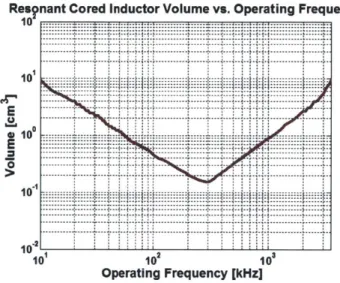
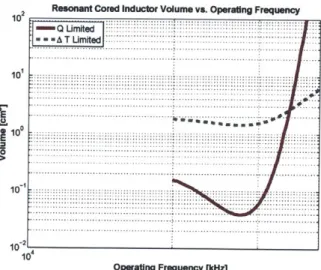
limited curve of Figure 2.2 shows the numerical optimization results and inductor box volume vs. design frequency. Note that box volume, as illustrated in [42], is the volume of the smallest box that the inductor could fit inside. The scaled inductor design achieves its minimum size at around 300 kHz, and beyond which the inductor volume increases drastically, with its minimum volume beingMagnetics Scaling
Resnant Cored Inductor Volume vs. Operating Frequency
10-... - - --... . . . . . ... - - . ...-- --- - 4- - - -... 10 -. E. -: -:: E *10 0 10 2 3 10 10 10 Operating Frequency [kHz]
Figure 2.2: Numerical Optimization results of inductor "box" volume vs. design frequency for an example resonant inductor
approximately 0.2 cm3. Figure 2.3 illustrates the two loss mechanisms of cored-inductors,
and their behaviors across the scaled frequency range. At low frequencies, winding loss contributes to a large portion of total loss, with flux density constrained primarily by saturation limits. However, at high frequencies, core loss increases significantly and the inductor core area must be increased to reduce flux density in order to maintain constant total loss and
Q
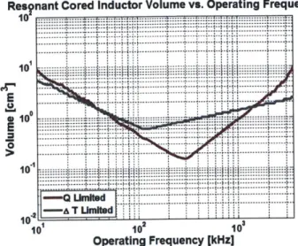
(loss budget). At frequencies where core loss is a factor limiting flux density (as opposed to flux density determined only by saturation limits), one ends up with flux density derated from the saturation limits by an amount that yields approximately equal core and winding loss.Also shown for comparison (Figure 2.4 are results for a separate CAD optimization which uses discrete, standard RM cores, wire sizes and gaps (with 3F3 material), incorporates multi-layer windings, and accounts for skin and proximity effect and core thermal limits, the inductor implemented here realizes an impedance of 157 £O (i.e. 250 piH at 100 kHz) at
Q
= 100 for 1 A peak ac current. We use a numerical search to optimize designs based on 3F3 core material. Results from this alternative optimization match well given differences in the design limits, and yield identical conclusions. We note that these results are qualitatively similar to those found for transformers in[46,47],
underscoring the limitations of frequency scaling in cored designs.2.4 Magnetics Scaling Analysis 10, 102 10 10"1 10
Loss and Flux Density vs. Frequency
: - - --- --- --- --- --- ---- --- -- --- -.-- - -- . . ----. ----. --- - - -- -t -- - ---4 t - -- - 4 -- --- -- -- --- -4 -- -i - - -- - - -i ----- ---4 - - -i --- ---t---4--t-t--- ->4--- ---- -- -- - -i- ---10 102 Operating Frequency [kHz]
10-Figure 2.3: Core loss and winding loss of an optimized resonant inductor vs. design fre-quency for a set of inductors realizing a constant impedance of 62.8 Q (i.e. 100 pH at 100 kHz) at
Q
= 100 for 1 A ac current. Numerical simulation files are included in Appendix A.10
1or
161,
Roeonan Core kductor Volume vs. Operin Prequeny
... . .. . .. .. .. .. ... . .... .4*4 ... .... ... .. .. . T.. .. U ... ed.... ... .. .. .... .. .. .. . 102
Operding Frequency pIHal
Figure 2.4: Numerical optimization results of inductor "box" volume (including discrete designs) vs. design frequency for a set of inductors realizing a constant impedance of 157
Q (i.e. 250 pH at 100 kHz) at
Q
= 100 for 1 A peak ac current. Numerical simulation files are included in Appendix A.10 1s I
10
Magnetics Scaling
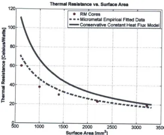
2.4.1.2 Temperature Constraint
It should be noted that there are also other constraints in miniaturization under frequency scaling. In the previous discussion, it is assumed that the inductor loss budget is the limiting factor for achieving a minimum volume. In addition to meeting a quality factor requirement, imposing a temperature rise limit on a given inductor may further increase its minimum achievable volume. In order to study how the volume of an inductor scales with a temperature rise constraint, a thermal model is first developed. Among the three heat transfer mechanisms (convection, conduction and radiation), the heat flow is proportional to surface area (of which the units are linear dimension squared) for convective and radiative heat transfer, whereas the heat flow through conduction is proportional to linear dimension if the dimensions of all structures are scaled together, ( 2.5). To form a conservative estimate at small scales, it is safe to assume that heat flow is at least proportional to the surface area and temperature rise, which corresponds to a constant heat flux limit for a given temperature rise, ( 2.6). qconvection = hA/AT oc e2 A AT qconduction = APT oC E (2.5) 1 PTH
qtotal (kiE2 + k2 6)AT
9tota
~kl6 2Zg(2.6) PDISS k1AAT
By matching the thermal resistance vs. surface area for this constant heat flux model
with discrete data points for RM type ferrite cores and an empirically-fitted curve for toroidal Micrometals cores [52], as shown in Figure 2.5 , we arrive at a heat flux limit of
6.7mW/(0C - mm2). This thus represents a thermal model which is quite conservative at small scales.
2.4 Magnetics Scaling Analysis
Thermal Resistance vs. Surface Area 120
0 RM Cores
- Micrometal Empirical Fitted Data
- Conservative Constant Heat Flux Model 100o 1 1... 2... 2.3.3.
~80
4 ... . .. . . ... . .. . . .. . . .. . . .. . .
9;0 1000 1500 2000 2500 300 3500 Surface Area [mm]
Figure 2.5: Thermal resistance vs. surface area for different data and models.
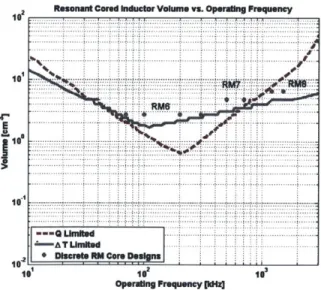
With this thermal model, a temperature limit of 400C is imposed on both previous inductor designs (i.e. 157Q and 62.8Q at 1 A ac current on a scaled RM core using 3F3 material). This AT limited curve of Figure 2.4 and Figure 2.6 plot the minimum size of an inductor that meets this temperature requirement without consideration of
Q.
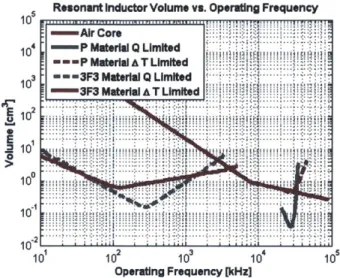
As shown in Figure 2.4 and Figure 2.6, both loss and temperature constraints are important, with an allowed design being on the maximum of the two curves.2.4.1.3 RF Low-Permeability Materials
As shown in Figure 2.6, resonant inductors constructed with conventional high permeability MnZn and NiZn ferrite materials, such as 3F3 and 3F4, are typically effective only up to a few megahertz, beyond which the volume must increase drastically to meet a given quality factor requirement. Introduction of low permeability rf materials (with several examples explored in [48,49,53]) extends the frequency range for which cored inductors are useful up to many tens of megahertz. However, core loss still imposes a fundamental frequency limit in minimizing size in resonant cored inductors built with rf materials, and there still exists an optimal frequency beyond which the inductor size increases in order to stay within a loss constraint. To demonstrate the efficacy of low-permeability RF materials, we simulate and optimize inductor designs for the same requirements (62.8f2 inductive impedance, 1 A ac current, a minimum
Q
of 100 and a maximum temperature rise of 40C ), using toroidsMagnetics Scaling
Resnant Cored Inductor Volume vs. Operating Frequency
10 .. 10'--- --- ---E10 --- t -4 0 100 . ... 10102 103 Operating Frequency [kHz]
Figure 2.6: Numerical Optimization results of inductor "box" volume vs. design frequency for an example resonant inductor with temperature limitations for a set of inductors realizing a constant impedance of 62.8 G2 (i.e. 100 piH at 100 kHz) at
Q
= 100 for 1 A ac current. Numerical simulation files are included in Appendix A.of P-type material (ps = 40) from Ferronics. The inductors designs are optimized based on a polynomial fit to the available core loss data [53] for P material and various toroidal core sizes [50]. Figure 2.7 illustrates that the box volume for inductors designed with P material is minimized near 30 MHz, with an achievable minimum size of ~~ 1.5cm3. Unlike the previous case, the minimum size in this example is limited by temperature rise. Figure 3 shows that, compared to designs with a conventional high-permeability material (i.e., 3F3), designs using an RF material (P) enables an approximate 40% reduction in volume to be achieved, along with a reduction of energy storage and increase in frequency by a factor of ~100. In other cases (e.g., higher temperature rise designs) the relative advantage of the
rf material would be even much larger.
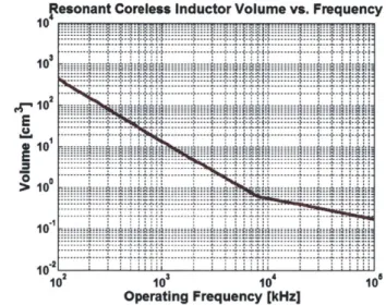
2.4.2
Coreless Inductor ScalingCore loss imposes fundamental frequency limits associated with minimizing size in cored resonant inductors. Since winding loss is the only major loss mechanism for a coreless design, coreless designs may offer a much better tradeoff between a given loss budget and volume at higher frequencies. In general, the inductance of a tightly-coupled magnetic structure can be expressed as being proportional to a linear dimensional scaling factor c
2.4 Magnetics Scaling Analysis
l Resonant Cored Inductor Volume vs. Operating Frequency 102. 10 101 101 102 Operating Frequency [kHz]
Figure 2.7: Resonant inductor volume comparison. The use of the rf material enables a ~ 40% reduction in volume as compared to using 3F3 material for this scaling example.
L = 1oc N2KE (2.7)
Consider a single-turn inductor: its inductance is directly proportional to the linear dimen-sion factor e (6), and its dc resistance is inversely proportional to e (7):
L = Kle (2.8)
Figure 2.8: Magnetic Dimension Scaling
Q Umited A T Umited, ... 4 . ... ... .. ... ... ... ... ... I ... ... ... ... ... ... .... .. ... ... ... ... ... .. .. . ... ... ... ... ... ... .... .. .. .... ... .. .. .. .. .. ... ... .. ... .. .. I ... ... I ... ... 4 0 ... ... ... ... ... .. ... ... ... ... ... .. ... ... ... .. .. .. .... .. ... ... ... ... ... .. .. .. .. . .. ... .. ... ... ... ... .... .... .... . ... ... .... ... -... .... ... ... .... ... ... ... ... .... ... ... ... ... - I ... ... ... ... I ... ... ... ... ... ... L ... ... ... .... ... ...
Magnetics Scaling
RDC =pl - K2 (2.9)
For ac resistance in the skin depth limit, the dependency on linear dimension is exchanged for a dependence on the square root of frequency:
d
RAC = d RDC = K3
<71
(2.10)For a closely-linked N-turn inductor, inductance, dc resistance and ac resistance are all merely scaled by number of turns squared.
L = N2KleRDc = N2K2 RAC = N2K3
f
(2.11)In order to scale an inductor design across frequency maintaining constant impedance and constant loss, we can first find the dependence of the quality factor on the linear scaling factor - and on frequency
27rf L 27rfN2Kie
Q
=
= = K4e (2.12)RAGc N2Kff
The quality factor is directly proportional to E and to the square root of frequency. Thus, to achieve a given impedance and quality factor as frequency is varied, an inductors linear dimension can be scaled as
f-
1/2, which in turns means that the volume of the inductor scales asf-3/
2. If quality factor were the only limiting factor, the required volume of a coreless inductor could be continuously reduced asf-3/
2as frequency increases. However, as the inductor volume (and surface area) gets smaller and smaller for a given loss, the inductor will eventually encounter its thermal (temperature rise) limit. From the thermal model developed in the previous section, imposing a temperature limit is equivalent to limiting heat flux through the inductor surface. Under this model, there are two ways through which the temperature rise can be decreased: reducing the loss and/or increasing the surface area. From ( 2.12), the quality factor is shown to be proportional to the linear
2.4 Magnetics Scaling Analysis
D
N: number of turns
Figure 2.9: Single layer coreless solenoid inductor
scaling factor. If the thermal model is combined with ( 2.12), the volume of a coreless inductor under a heat flux limit scales with
f
-1/2:AT= k Pdiss - k IRMS - k IRMSZ (2.13)
Areasurface AreaSurf ace
Q
e2 fTherefore, even in the heat flux (thermally) limited case, the volume of an air-core inductor can still be made smaller with increasing frequency. Furthermore, the quality factor of the inductor in the heat-flux-limited scaling actually improves as fi/3. This scaling can
be maintained so long as at least one turn or more is required for the desired impedance at the specified scale. (Scaling can still be achieved beyond this point in some cases, but necessitates changes in geometry.)
2.4.2.1 Coreless Inductor Design Example
For a single layer coreless solenoid inductor, a good empirical model is available based on Medhurst's work [54-57]. In Medhurst's model, quality factor
Q
is directly proportional to the diameter of a solenoid, square root of frequency and another factor IF, where T is a function of length 1 to diameter D of the solenoid and wire diameter to wire spacing:Q
m 7.5D' T/fWotimum 0.96 tanh(O.86 -