HAL Id: tel-02902102
https://tel.archives-ouvertes.fr/tel-02902102
Submitted on 17 Jul 2020
HAL is a multi-disciplinary open access
archive for the deposit and dissemination of sci-entific research documents, whether they are pub-lished or not. The documents may come from teaching and research institutions in France or abroad, or from public or private research centers.
L’archive ouverte pluridisciplinaire HAL, est destinée au dépôt et à la diffusion de documents scientifiques de niveau recherche, publiés ou non, émanant des établissements d’enseignement et de recherche français ou étrangers, des laboratoires publics ou privés.
Maiglid Andreina Moreno Villavicencio
To cite this version:
Maiglid Andreina Moreno Villavicencio. Development of 3D high-resolution imaging of complex de-vices by the correlation of ToF-SIMS and AFM. Electronics. Université de Lyon, 2019. English. �NNT : 2019LYSEI122�. �tel-02902102�
Opérée au sein de
INSA Lyon
Ecole Doctorale N° ED160
Électronique, Électrotechnique et Automatique
Spécialité de doctorat :Micro et nano technologies
Soutenue publiquement le 03 / 12 / 2019 par :Maiglid Andreina Moreno Villavicencio
Développement de l’imagerie 3D haute résolution
par ToF-SIMS et AFM de dispositifs avancés
Devant le jury composé de
Leonard, Didier PU - Université Claude Bernard Lyon 1 Président Galtayries, Anouk MC - Chimie ParisTech Rapporteure Conard, Thierry Ingénieur de recherche - IMEC Rapporteur Valle, Nathalie Ingénieur de recherche - LIST Examinatrice Fearn, Sarah Chargée de recherche - Imperial College Examinatrice
Gautier, Brice PU INSA Lyon Directeur de thèse
RÉSUMÉ
Développement de l’imagerie 3D haute résolution par ToF-SIMS et AFM de
dispositifs avancés
La miniaturisation continue et la complexité des dispositifs poussent les techniques existantes de nano-caractérisation à leurs limites. De ce fait, la combinaison de ces techniques apparait être une solution attrayante pour continuer à fournir une caractérisation précise et exacte. Dans le but de dépasser les verrous existants pour l’imagerie chimique 3D haute résolution à l’échelle nanométrique, nous avons concentré nos recherches sur la création d’un protocole combinant la spectrométrie de masse à ions secondaires de temps de vol (ToF-SIMS) avec la microscopie à force atomique (AFM). Ceci permet entre autres de corréler la composition et la visualisation en 3 dimensions avec des cartographies de topographie ou d’autres propriétés locales fournies par l’AFM. Trois principaux résultats sont obtenus grâce à cette méthodologie : la correction d’un ensemble de données ToF-SIMS pour une visualisation 3D sans artefacts, la cartographie du taux de pulvérisation locale permettant de mettre en évidence les effets liés à la rugosité et la présence d’interfaces verticales et la superposition des informations avancées ToF-SIMS et AFM.
Quatre applications de la méthodologie combinée ToF-SIMS et AFM sont abordées dans cette thèse. La procédure de correction des données ToF-SIMS en 3D a été appliquée sur une structure hétérogène GaAs / SiO2. Les artefacts liés à la pulvérisation, notamment l’effet d’ombrage, ont
été étudiés par le biais des cartographies de taux de pulvérisation sur des échantillons avec nano-motifs structurés et non structurés. Enfin, nous avons exploré la combinaison de l’analyse ToF-SIMS avec trois modes avancées de microscopie AFM : piézoélectrique (PFM), capacité (SCM) et conducteur (SSRM). Une première étude a notamment permis d’observer l’évolution et la modification chimique suite à l’application d’une contrainte électrique sur deux films minces piézoélectriques. Une deuxième étude s’est focalisée sur l’impact de l’implantation Ga lors de la préparation d’échantillons par FIB pour voir comment limiter l’effet de l’amorphisation sur la mesure électrique. Les aspects techniques de la méthodologie sont abordés pour chacune de ces applications et les perspectives de cette combinaison sont discutés.
Mots-Clés: AFM – ToF-SIMS – caractérisation chimique 3D – PFM – SCM – SSRM
corrélation et combinaison de techniques – reconstruction et visualisation 3D – effets d’ombrage – cartographie de vitesse de pulvérisation – overlay ToF-SIMS et AFM.
ABSTRACT
Development of 3D high-resolution imaging of complex devices by the
correlation of ToF-SIMS and AFM
The continuous miniaturization and complexity of devices have pushed existing nano-characterization techniques to their limits. The correlation of techniques has then become an attractive solution to keep providing precise and accurate characterization. With the aim of overcoming the existing barriers for the 3D high-resolution imaging at the nanoscale, we have focused our research on creating a protocol to combine time-of-flight secondary ion mass spectrometry (ToF-SIMS) with atomic force microscopy (AFM). This combination permits the correlation of the composition in 3-dimensions with the maps of topography and other local properties provided by the AFM. Three main results are achieved through this methodology: a topography-corrected 3D ToF-SIMS data set, maps of local sputter rate where the effect of roughness and vertical interfaces are seen and overlays of the ToF-SIMS and AFM advanced information.
The application fields of the ToF-SIMS and AFM combined methodology can be larger than expected. Indeed, four different applications are discussed in this thesis. The procedure to obtain the topography-corrected 3D data sets was applied on a GaAs / SiO2 patterned
structure whose initial topography and composition with materials of different sputter rates create a distortion in the classical 3D chemical visualization. The protocol to generate sputter rate maps was used on samples with structured and non-structured nano-areas in order to study the possible ToF-SIMS sputtering artefacts, especially the geometric shadowing effect. Finally, we have explored the combination of ToF-SIMS analysis with three AFM advanced modes: piezoresponse force microcopy (PFM), scanning capacitance microscopy (SCM) and scanning spreading resistance microscopy (SSRM).Specifically, two main applications were studied: the chemical modification during electrical stress of a piezoelectic thin film and the recovery of initial electrical characteristics of a sample subjected to Ga implantation during FIB preparation. Technical aspects of the methodology are discussed for each application and the perspectives of this combination are given.
Keywords: AFM – ToF-SIMS – 3D chemical characterization – PFM – SCM – SSRM –
correlation and combination of techniques – 3D reconstruction and visualization – geometric shadowing effect – sputter rate map – ToF-SIMS and AFM overlay.
CONTENTS
RÉsumÉ iv
Abstract vi
Contents viii
Abbreviation index xiii
List of Figures xv
CHAPTER I. Introduction to high resolution 3D chemical characterization of microelectronic
devices 19
1. Microelectronic technology 20
2. Three-dimensional characterization and chemical imaging 24 2.1. Beyond the ToF-SIMS challenges by its combination with the Atomic force
microscopy 27
3. ToF-SIMS and AFM as a combined approach to characterize microelectronic devices 29
4. Thesis outline 31
5. Conclusions 33
CHAPTER II. ToF-SIMS and AFM as individual characterization techniques and their
combined protocol 35
1. Time-of-Flight secondary ion mass spectrometry 36
1.1. General principle 37
1.2. Ion-solid interactions 41
1.3. Time-of-Flight mass analyzer 42
1.4. Instrumental setup 43
2. Atomic force microscopy 45
2.1. General principle 45
2.2. AFM scanning modes 48
3.2. Ex-situ ToF-SIMS / AFM instrumentation 58
4. Combined ToF-SIMS and AFM methodology 60
4.1. Sample preparation and previous analysis 62
4.2. Cyclical ToF-SIMS / AFM / profilometer analysis 62
4.3. Raw data treatment 64
4.4. Advanced data processing 66
5. Conclusions 71
CHAPTER III. Combined ToF-SIMS and AFM protocol for a topography-corrected 3D chemical
visualization and depth-profiles 73
1. 2D ToF-SIMS images and the 3D visualization 74
1.1. Challenges and artefacts 75
1.2. Solutions and approaches 78
2. Proposed ToF-SIMS and AFM combined methodology to correct the 3D ToF-SIMS
visualizations and depth-profiles 80
2.1. Overlay of the chemical information over topographical surfaces 83
2.2. Calculation of sputter rate maps 84
2.3. Topography-corrected 3D chemical visualization 86
2.4. Results and their 3D visualization 90
3. ToF-SIMS / AFM combined methodology applied on a GaAs / SiO2 patterned
structure 92
3.1. Sample description 93
3.2. Analysis conditions 94
3.3. Experimental section 94
3.4. Data processing 96
3.5. Results of the ex-situ methodology 98
3.6. Results of the in-situ ToF-SIMS and AFM combined methodology 105
4. Conclusions 108
CHAPTER IV. Studying the sputtering phenomenon of nanostructures with ToF-SIMS and
1. What really happens during sputtering and analysis of nanostructures? 112 1.1. Impact of the primary energy on sputter yield, roughness and depth resolution 114 1.2. Impact of the primary beam orientation on the lateral resolution, shadowing effect and topography evolution of the vertical interfaces 118
2. Chemical analysis of non-structured nano-areas 124 2.1. Sample description and preliminary analysis 125
2.2. Advanced characterization of nano-cracks 126
3. Conclusions 133
CHAPTER V. Combining ToF-SIMS with AFM electrical modes 135 1. ToF-SIMS with advanced AFM operation modes. Is it a novel combination? 136 2. ToF-SIMS and PFM combined methodology to study the chemical modification of
piezoelectric samples after local polarization 138
2.1. Experimental protocol and analysis conditions 139 2.2. Results of the non-ferroelectric LAO sample 144
2.3. Results of the BTO ferroelectric sample 150
2.4. Propositions for future work 152
3. Measuring and recovering electrical properties of doped samples with ToF-SIMS
and SCM / SSRM 154
3.1. Sample description and preliminary protocol 156 3.2. Results of the non-patterned silicon substrates 160
3.3. Results of the patterned samples 164
3.4. Proposed protocol for future work 166
4. Conclusions 168
Final conclusion and perspectives 170
Bibliography 175
Appendix 189
A.1. Formation of Cs+ aggregates at the sample surface 189
1. Méthodologie d’Analyse Combinée ToF-SIMS et AFM 195
1.1. Traitement des données brutes 196
1.2. Alignement et redimensionnement des données 197
1.3. Principaux résultats 199
2. Application de la méthodologie combinée AFM – Tof SIMS 203 2.1. Description de l’échantillon et conditions d’analyse 203
2.2. Descriptif expérimental 204
2.3. Superposition ToF-SIMS et AFM 205
2.4. Cartographie de vitesse de pulvérisation 206
2.5. Visualisation 3D des données ToF-SIMS corrigées 207 3. Étude du processus de pulvérisation sur des nanostructures à l'aide de la
méthodologie combinée AFM/ToF-SIMS 209
3.1. Résultats sur les motifs carrés de SiO2 210
3.2. Analyse d’un empilement SiN/AlN/GaN 213
4. ToF-SIMS combiné avec les modes AFM électriques 217 4.1. Etude de la modification chimique d’échantillons piézoélectriques après
polarisation électrique locale 217
4.2. Mesure et récupération des propriétés électriques d'échantillons dopés par
TOF-SIMS et SCM/SSRM 221
ABBREVIATION INDEX
2D Two-dimensional
3D Three-dimensional
AFM Atomic force microscopy
C-AFM Conductive-atomic force microscopy
CPD Contact potential difference
CMOS Complementary-metal-oxide-semiconductor
DFRT Dual frequency resonance tracking
EDX Energy-dispersive X-ray spectroscopy
EELS Electron-energy-loss spectroscopy
FTIR Fourier-transform infrared spectroscopy
FWHM Full width at half maximum
GSI Gigascale-scale integration
KFM Kelvin force microscopy
LMIS Liquid metal ion source
METRO 4-3D Metrology for future 3D-technologies
MFM Magnetic force microscopy
MOCVD Metal organic chemical vapor deposition
MOS Metal-oxide-semiconductor
MSI Medium-scale integration
PCA Principal component analysis
PFM Piezoresponse force microscopy
PFT Peak force Tapping
PI Feedback Proportional-integral feedback system
ROI Region of interest
SIMS Secondary ion mass spectrometry
SOC System on a single chip
SSI Small-scale integration
SSRM Scanning spreading resistance microscopy
STEM Scanning transmission electron microscopy
TEM Transmission electron microscopy
ToF-SIMS Time-of-flight secondary ion mass spectrometry
XPS X-ray photoelectron spectroscopy
LIST OF FIGURES
Figure I.1 - Evolution of microelectronics. 21
Figure I.2 - Analytical resolution vs. detection limit of most common characterization
techniques. 26
Figure I.3 - Advanced AFM operation modes. 28
Figure II.1 - Schematic of ToF-SIMS dual beam instrument. 38
Figure II.2 - Schematic of ToF-SIMS 3D analysis. 38
Figure II.3 - Force – distance curve. 45
Figure II.4 - Schematic of the AFM principle and components. 46 Figure II.5 - Resonance curve for a single harmonic oscillator. 49
Figure II.6 - MOS capacitor system. 51
Figure II.7 - Schematic of piezoelectric behavior under electric field. 54 Figure II.8 - Schematic of the ToF-SIMS and AFM combined methodology. 61 Figure II.9 - Schematic of the ToF-SIMS raw data processing. 64 Figure II.10 - Schematic of the profilometer raw data processing. 65 Figure II.11 - Schematic of the AFM raw data processing and displacement AFM profiles. 66 Figure II.12 - Schematic of the pixel size correction. 67 Figure II.13 - Schematic of the alignment process. 68 Figure II.14 - Table of compatibility created using normalized-cross-correlation. 69 Figure II.15 - Combined ToF-SIMS / AFM in-situ instrument. 57 Figure II.16 - Instrument for the ex-situ approach. 59 Figure III.1 - Aberrations of ToF-SIMS images created by the sample topography. 76 Figure III.2 - Distortion of 3D visualization when stacking 2D ToF-SIMS images. 77 Figure III.3 - Approaches to correct the 3D ToF-SIMS data visualization. 79 Figure III.4 - Exemplary ToF-SIMS and AFM data set. 82 Figure III.5 - Schematic of the overlay procedure. 84
Figure III.6 - Schematic of sputter rate maps. 85
Figure III.9 - Schematic of the relocation of the ToF-SIMS images intensities within the
reconstructed volume of each element. 89
Figure III.10 - GaAs layer grown in a SiO2 cavity. 93 Figure III.11 - Combined ToF-SIMS / AFM methodology on a GaAs based sample. 95 Figure III.12 - Schematics of the data processing steps. 96 Figure III.13 - Resizing the AFM and the ToF-SIMS images to obtain the same pixel size. 97 Figure III.14 – Alignment of ToF-SIMS images for the ex-situ procedure. 98 Figure III.15 - AFM and ToF-SIMS overlay for each cycle stage. 99 Figure III.16 - Topography profiles of AFM image sections. 100 Figure III.17 - Sputter rate maps [nm/s] of the GaAs / SiO2 structure. 102 Figure III.18 - Stack of ToF-SIMS images for the ex-situ procedure. 103 Figure III.19 - Alignment of ToF-SIMS images for the in-situ procedure. 106 Figure III.20 - Front view of the topography-corrected stack of ToF-SIMS images. 107 Figure IV.1 - AFM images of the “squares” SiO2 patterns with GaAs confined inside them. 114 Figure IV.2 - Influence of the primary energy on the sputter yield and surface roughness. 116 Figure IV.3 - AFM initial images of the SiO2 lines separated by GaAs. 118 Figure IV.4 - Influence of the primary beam orientation on the lateral resolution of ToF-SIMS
imaging. 119
Figure IV.5 - Influence of the beam orientation on the sputtering rate of the sample. 121 Figure IV.6 - Influence of the primary beam orientation on the topography evolution at the
interfaces. 122
Figure IV.7 - AlN / GaN heterostructure. 125
Figure IV.8 - High lateral resolution 3D ToF-SIMS analysis of the AlN / GaN structure. 127 Figure IV.9 - 3D non-corrected visualization of the ToF-SIMS data. 128 Figure IV.10 - AFM topographical images captured in areas of the beveled crater. 130 Figure IV.11 – Initial and final AFM topographical images. 131 Figure IV.12 - STEM and EDX images of a SiN / AlN / GaN structure. 132 Figure V.1 - PFM phase image of PZT, LAO, BTO, Al2O3. 140
Figure V.2 - Amorphous LAO structure 141
Figure V.4 - KFM images of the LAO structure. 145 Figure V.5 - Results of the second analysis of the LAO sample. 146 Figure V.6 - Results of the third analysis for the LAO sample. 147 Figure V.7 - PCA scores and loadings of the second LAO analysis. 148 Figure V.8 - PCA scores and loadings of the second LAO analysis. 149 Figure V.9 - Lanthanum normalized intensity and depth-proffiles obtained from the third LAO
analysis. 150
Figure V.10 - Results of the first analysis and second analysis of the BTO sample. 151
Figure V.11 – N-doped silicon substrate. 158
Figure V.12 – Doped silicon patterned samples. 159
Figure V.13 - Results of the first non-patterned sample. 161 Figure V.14 - AFM initial topography and cross sections profiles. 161 Figure V.15 - Results of the second non-patterned sample. 162 Figure V.16 - ToF-SIMS depth profiles of the gallium implanted areas. 163 Figure V.17 - Results of the first patterned sample. 164 Figure V.18 - Results of the second patterned sample. 166 Figure A.1 - AFM topographical images showing the Cs+ aggregates at the SiO2 surface. 161 Figure A.2 - Tip convolution in AFM profiles. 162 Figure A.3 - AFM profiles of the sample captured scanning at 0 and 90 degree. 163
CHAPTER I.
INTRODUCTION TO HIGH RESOLUTION 3D CHEMICAL
CHARACTERIZATION OF MICROELECTRONIC DEVICES
This chapter introduces microelectronic technology, its beginning and its challenges. It describes how its development has been important for every field of science and the spread of applications that it has had. The author addresses the importance of reliable characterization instruments that can assure the good performance of micro devices, especially those that can provide chemical information in three dimensions (3D). The pros and cons of using time-of-flight secondary ion mass spectrometry (ToF-SIMS) as a 3D chemical characterization technique are discussed. The chapter presents the atomic force microscopy as a correlative technique to overcome some of the ToF-SIMS limitations. It presents the state-of-the-art of this ToF-SIMS / AFM combination and details its advantages. The chapter concludes with the outline of the information found in this manuscript.
1.
M
ICROELECTRONIC TECHNOLOGYMicroelectronics is the area of technology that uses small elements to manufacture electronic systems. It emerged from the need of less expensive, lighter and smaller electronic devices such as radar, communication and missiles guidance systems.
The evolution of microelectronics is shown in Figure I.1.a. Microtechnology started in 1948 when John Bardeen, William Shockley and Walter Brattain created the first transistor. Three years later, this device would completely replace the electron tubes that electronic systems were using at that time. The transistors were fabricated with semiconductor materials such as germanium and doped monocrystalline silicon. Their size started no bigger than a fingertip and they are now three thousand times smaller than a human hair. They have evolved from lateral dimensions of 10 µm to 45 nm in forty years. Indeed, current production is seeking lateral dimensions down to 7 nm. [1,2]
The reliability of electronic systems, already complex by that time, was not improved by the addition of many small discrete components named transistors. To overcome this issue, in 1959, six of those circuit components were associated as a unit on a single substrate introducing the integrated circuits in the market. Transistors started to be manufactured directly on silicon surface, ten transistors forming the small-scale integration (SSI), one thousand of them in the medium-scale integration (MSI) and soon, ten millions of transistors in a gigascale-scale integration (GSI).
Integrated circuits were created to satisfy the demand of size and weight reduction, as well as a diminution of the number of connections in individual systems. Modern devices are only a few atoms tall and use metal-oxide-semiconductor (MOS) and complementary-metal-oxide-semiconductor (CMOS) technology.
Some modern electrical devices are not only integrated circuits but also integrated systems; they may have all the components needed by the system on a single chip (SOC) [5]. The wide applications of these powerful integrated circuits created the market of modern electronics: miniaturized, digital and intelligent electronic products with low energy consumption, good quality, reliability and a fair price-performance ratio. Figure I.1.b shows the evolution of transistor price and the density of integrated circuits in the past 20 years. The transistor’s price has decreased from 1 to 10-7 dollars since 1968. This price reduction is associated to the development of integrated systems with more and smaller transistors. The number of transistors per unit area quadrupled every three years and the price of circuits were reduced by half every 18 months. At the same time, the productivity gains were about 30% every year positioning the electronic industry at the top of the national economy in several countries. [6,7]
The key of the growing market is the investment in innovation to conceive faster, smaller, and more efficient devices; more transistors per area, more functions per area and less cost per function. Electronics started in radio, television and military devices such as weapons, navigation, communications and radar systems. Nowadays, microelectronics is present in the majority of electronic devices. They are found in our offices, in our household goods, in the gadgets that we use to communicate and to entertain us, in the hospitals and in our transportation systems [8]. Bargon [1] illustrated, seven years ago, the applications for microelectronics in every existing market. However, the applications are constantly improved and spread to other markets where consumer demands need to be satisfied: medicine, energy, aerospace, plastics, etc. [6]
These developments came with challenges and complexity. In 1965, Gordon Moore, cofounder of Intel Corporation, the largest semiconductor chip manufacturer, predicted that the semiconductor technology would duplicate its effectiveness every 18 months. Expecting that for 2020, the microelectronic technology will reach a scale of 14 nm. This surprisingly accurate prediction was named “Moore’s law”. [9]
This progress is not only seen in the reduction to nanometer scale but also in the new materials, structures, circuit design, working environment and the evolution of the processing techniques. The precision, quality control and the final product inspection were vital in the improvement of manufacturing. Indeed, the accuracy and reliability of production machines and measuring instruments were decisive factors in the development of the microelectronics industry. [6]
The need for qualitative and quantitative information of nano-devices introduced high quality, reliable and sophisticated characterization techniques. These nanocharacterization techniques allowed to study, throughout the synthesis and processing of nano-devices, the topographical surfaces, morphology, crystal structure, particle size, existing defects and their chemical composition at the nano-scale [10,11]. Furthermore, the continuous fabrication of 3D architectures at a scale where their lateral dimensions have approached their third dimension renders impossible the full comprehension of the system without the analysis of all three dimensions. [12]
2.
T
HREE-
DIMENSIONAL CHARACTERIZATION AND CHEMICAL IMAGINGThe need for high-resolution chemical and molecular characterization in two and three dimensions has emerged simultaneously in diverse fields of science. The development of chemical imaging in the 70s [13] had an important impact on the optimization of the
microstructure for composites materials, on the knowledge of biological structures, on the analysis of mechanical, magnetic and electrical phenomena at small scales, on the functionality of micro and nano devices and on the examination of dopant profiles of microelectronic systems. [14,15]
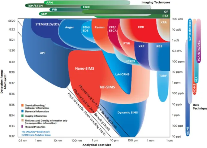
Figure I.2 presents the most common characterization techniques classified in colors by the information that they provide: imaging techniques in green, physical properties in violet, thickness and density in beige, elemental information in blue and molecular information in red. The utilization of them in physical, material, biological sciences, etc. depends primary on their non-destructive nature, affinity to certain material, spatial resolution and the detection range. [15]
Despite the multiples techniques shown in the graph, only a few of them can determine 3D molecular information or have been adapted to provide 3D chemical imaging. The most used techniques with their limitations are described below.
- Electron tomography: an electron microscopy technique that produces a 3D rendering from two-dimensional (2D) projections of the sample. The object is tilted inside the microscope to obtain a projection of the chemical composition along the electron trajectory. From the 2D projections (typically 1 nm spatial resolution), a reconstruction algorithm creates the 3D matrix of the sample in the real space. Depending on the electron microscopy mode selected to obtain the chemical composition and images [energy-dispersive X-ray spectroscopy (EDX), electron-energy-loss spectroscopy (EELS), electron holography, among others], there are restrictions for the detection of the chemical information and huge challenges when imaging soft materials. Furthermore, electron tomography requires sample preparation to reduce the sample thickness down to a few hundreds of nanometers. [14–16]
- NanoSIMS: uses the principle of dynamic SIMS to obtain elemental and isotopic information with a lateral resolution down to 50 nm. A primary ion beam bombards the surface and the secondary ions are separated using a magnet. The disadvantage of this technique is that only seven different masses can be separated and detected. [17]
- Atom probe tomography: it is a combination of field ion microscopy with a mass spectrometer. It was created to perform chemical measurements and imaging at the atomic scale (down to 0.3 nm in lateral resolution and 0.1 nm in depth resolution). It consists in the evaporation and ionisation of the sample atoms using a pulsed laser. The ions are projected onto a 2D detector where their flight time and x,y localization are registered. Reconstruction algorithms use the x,y localization to obtain 3D visualization of the sample. The main disadvantage of this technique is the sample preparation and thus the low detection range (at the best conditions 5.1018 at/cm3). The sample has to be transformed into a very sharp tip with an end-radius between 10 and 100 nm. [18,19]
- 3D time-of-fight-secondary ion mass spectrometry (ToF-SIMS): it was initially created to image the elemental information of surfaces through the detection of secondary ions sputtered from the sample using a primary ion beam. A second ion beam was integrated to the system in order to remove the already analyzed surface and expose a new one.
Figure I.2 Analytical resolution vs. detection limit of most common characterization techniques. They are classified in colors depending on the information that they provide. Image extracted from EAG Evans Analytical Group. [16]
A chemical image of the new surface is obtained and an in-depth chemical analysis is performed. The stack of those ToF-SIMS images creates a 3D representation of the sample. This technique does not require sample preparation and its depth resolution can be as good as 1 nm. It has a dynamic range and high mass resolution, up to 104 M/ΔM. However, its lateral resolution is only 100 nm.
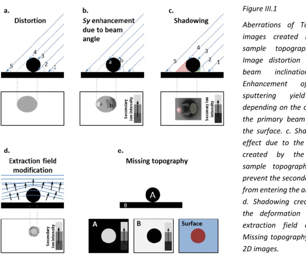
Additionally, challenges with the 3D reconstruction and the sputtering of inhomogeneous samples remain because the standard ToF-SIMS data reconstruction method does not take into the account the sample topography.
ToF-SIMS is a suitable technique to analyze complex stacks of thin organic and inorganic layers, devices with different compositions, samples with strong topography, patterned structures, among others. It is widely used in the microelectronics, biology, metallurgic and pharmaceutical fields for the identification of contamination, failure analysis, and evaluation of fabrication process and quantification of dopants. [20–22]
However, in microelectronics, the use of a large variety of materials in increasingly complex structures drove this technique to its limit in resolution. For many analytical questions, a combined characterization approach seemed more reliable. Some authors have combined the ToF-SIMS with techniques shown in the top left of the graph in Figure I.2 as a solution to improve the lateral resolution of the chemical imaging. Association of ToF-SIMS with several techniques and novel sample preparation as X-ray powder diffraction (XRD)
[23,24], X-ray photoelectron spectroscopy (XPS) [25–27], Fourier-transform infrared spectroscopy (FTIR) [28], scanning electron microscopy (SEM) [29], atom probe tomography
[30], and transmission electron microscopy (TEM) [31] are found in the literature. However, the
combination of ToF-SIMS with atomic force microscopy (AFM) is found to be the key for the 3D high-resolution imaging of complex microelectronic devices.
2.1. B
EYOND THET
OF-SIMS
CHALLENGES BY ITS COMBINATION WITH THEA
TOMIC FORCE MICROSCOPYThe AFM is largely used to image the surface topography of organic, inorganic and biomaterials. Topographical maps are created using the interaction force between a nanometric tip and the sample surface. The lateral resolution of 10 nm and the depth resolution of 0.1 nm turned the AFM into the instrument most utilized to manipulate and visualize surface properties at the nanoscale.
This technique opens the possibility of compensating the ToF-SIMS lateral resolution and at the same time, contributes the topographical information that is missing in the 3D reconstruction algorithm. Furthermore, the versatility of AFM as a characterization technique through the modification of the tip, allows it to image local properties of the sample. Figure
Conductive-atomic force microscopy (C-AFM) and Kelvin force microscopy (KFM) measure, respectively, the current between the tip and the sample and the tip-surface contact potential as function of an applied bias within dielectric thin films, dynamic random access memories, etc. [33,34]. Distinct operation modes were also developed to investigate the electromechanical response for piezoelectric films, mechanical response of soft samples and magnetic properties of microdevices. However, none of the existing modes provides molecular or elemental information.
Naturally, the interest of the scientific community on correlating the chemical and the topographical has increased with the years bringing the development of other combined instruments such as AFM with scanning electron microscopes (SEM) or with a NanoSIMS, unique instruments that enable the complementarity of these other techniques [36,37].
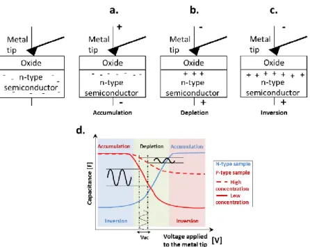
The AFM advanced modes have been implemented in the routine characterization of microelectronics since their development in the late 80s. Electrical modes such as scanning capacitance microscopy (SCM) and scanning spreading resistance microscopy (SSRM) are used to image dopant distribution and concentration within semiconductors [32].
3.
T
OF-SIMS
ANDAFM
AS A COMBINED APPROACH TO CHARACTERIZE MICROELECTRONIC DEVICESThe ToF-SIMS and AFM have been complementary techniques for more than 20 years in diverse fields of science. They were initially combined to relate surface roughness or morphology to sample composition. This combination has contributed in different ways to the understanding of many phenomena. A few examples are listed below.
- Physics of sputtering: study of inhomogeneity and damage produced by the ToF-SIMS sputtering through the measurement of the surface roughness by AFM [38–40]. Indeed, some authors have compared the damage and the ion-induced topography created by different ToF-SIMS sputtering conditions using AFM analysis in order to set the most suitable conditions for specific analysis [41–43].
- Polymers and organic molecules: study of phase formation, lamellar orientation, molecules aggregation and their distribution into the sample. [44–47]
- Biomolecules and cells chemical imaging: study of biochemical surface patterning, composition of human cells. [48,49]
- Inorganic samples: study of surface contamination or molecule absorption from the environment to metal surfaces, defects existing in interfaces and surfaces of inorganic samples. [50,51]
The research community is attracted by this combination and they are currently using it to advanced characterization of complex samples using diverse operation modes of AFM. - Conductive-AFM and ToF-SIMS: study the electroforming behavior in resistive switching
cells, hysteresis of solar cells. [52,53]
- Piezoresponse force microscopy (PFM) and ToF-SIMS: study of polarization switching in ferroelectric materials. [54,55]
- KFM and ToF-SIMS: correlation of hydrophilic, hydrophobic and charged regions with their chemical composition, study of surface potential and morphology control of organic solar cells. [56,57]
- SCM – SSRM and ToF-SIMS: study of carrier concentration profiles and atomic diffusion within layers. [58,59]
- Chemical modification of AFM tip and ToF-SIMS: study of end groups of molecules present on the sample surface, the determination of any specific recognition of those molecules and their distribution over the surface. [60]
The AFM has also emerged as a solution to overcome the artefacts found in a 3D ToF-SIMS analysis. It is a suitable characterization technique to provide the missing topography to the 3D ToF-SIMS reconstruction. [61,62]
The ToF-SIMS / AFM combination started ex-situ, but an analysis can be time consuming. The sample transfer, the pumping time and the area localization will add about 30 minutes each time a transfer is needed. The duration of a complete analysis depends on the individual time needed to perform common AFM images, common ToF-SIMS depth profiles but also on the transfer time between the two analysis positions. Additionally, the sample transfer needs to be done in a controlled environment to reduce the contamination of the surface.
Arising from the expansion of applications for these two techniques, in 2008 a European project named 3D NanoChemiscope started. Its goal was to develop a combined ToF-SIMS / AFM instrument for the three dimensional chemical analysis of nanostructures. This single ultra-high vacuum instrument would provide information, on the nanoscale, about surface chemistry and surface morphology from the same sample region [63].
The entry of this instrument on the market opened the possibility of performing in-situ analysis with less contamination or surface degradation; the sample remains in the vacuum chamber. The precision of the sample transfer between the instruments is assured by the integrated piezo displacement system allowing analysis to be performed on the same sample area. Additionally, the sample only needs to be pumped down once. However, depending on the AFM operation mode, good quality topographical images under vacuum can take days. Although ex-situ and in-situ methodologies have their advantages and inconveniences both can achieve similar results.
Further investigation of the application fields of combined characterization techniques is being carried out by laboratories around the world. A European project was created in 2016 under the name “Metrology for future 3D-technologies” (METRO 4-3D) in which ten European laboratories studied the applications of correlative characterization techniques in semiconductor 3D-structures and devices [64]. Part of the work in this manuscript was performed as part of this European programme and it has received funding from the European Union’s Horizon 2020 research and innovation programme under grant agreement No 688225.
This thesis project aims the development of a combined ToF-SIMS / AFM methodology that allows a correlation of the chemical and topographical information of advanced devices. It studies several applications of this combination while answering current challenges that the individual techniques present. The project was held at the NanoCharacterization Platform of CEA Grenoble. However, it benefited from the in-situ ToF-SIMS / AFM instrument located at IMEC in Belgium and the data treatment knowledge of the EMPA group located in Switzerland.
4.
T
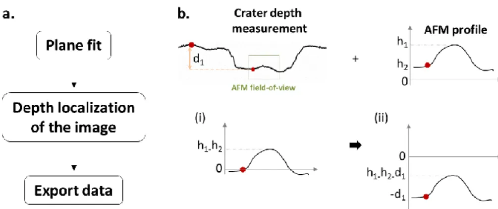
HESIS OUTLINECHAPTER II of this thesis project presents in detail a combined ToF-SIMS and AFM methodology that can be used in the microelectronic field. The methodology comprises AFM topographical images, crater depth measurements and sequences of ToF-SIMS images, all acquired on the same area of the sample. The principle is to perform AFM images and crater depth measurements every time an interface is detected in the ToF-SIMS depth-profile. These intermediate AFM images can be used to estimate the sample surface topography and roughness at different points of the depth profile, matching each value to their corresponding chemical element at that depth. In the case where AFM advanced operation modes are used, a combination of three types of information is possible: chemical, topographical and the property provided by the advanced mode. In addition, the intermediate AFM images allow the calculation of pixel-per-pixel sputter rates and provide further knowledge about the sputtering behavior of 3D systems. [65,66].
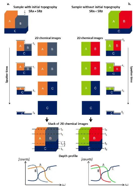
CHAPTER III describes the process to correct the 3D ToF-SIMS visualization of a GaAs / SiO2 heterogeneous sample using the established ToF-SIMS and AFM combined methodology. The initial topography of the sample and the high difference of sputter rates between the GaAs and the SiO2 creates a distortion of the ToF-SIMS data set when performing a classical 3D visualization. In the same way, local sputter rate maps of the analyzed area were calculated and the lateral variation of sputter rates was analyzed using the AFM topographical profiles. Moreover, overlay of the chemical elements over topographical surfaces allowed the correlation of the chemical composition with surface roughness and morphology.
The ToF-SIMS and AFM procedure to obtain local sputter rate maps was used to study the artefacts found when performing ToF-SIMS analysis of nano-structures. CHAPTER IV starts analyzing the optimization of the analysis conditions when sputtering nano-patterns. Specifically, the influence of the primary energy and beam orientation on sputter yield, sample roughness, lateral and depth resolution and topography evolution. It introduces the term geometric shadowing effect that was sequentially studied for an AlN / GaN heterostructure with cracks on all over the surface.
Finally, three AFM advanced operation modes are introduced in CHAPTER V. They are piezoresponse force microscopy (PFM), scanning capacitance microscopy (SCM) and scanning spreading resistance microscopy (SSRM). Specific protocols for the experiments are described. The chapter starts with the combination of PFM with ToF-SIMS. It was used to analyze the chemical modification produced during electrical stress of piezoelectric thin films. The chemical effect of the contact of the AFM tip with the surface is also investigated.
Secondly, the results obtained through the combination of ToF-SIMS with AFM electrical modes such as SCM and SSRM are presented. The ToF-SIMS sputtering was used to remove from an n-p-doped sample the gallium implantation from FIB preparation and thus, recover the initial electrical characteristics.
The thesis manuscript ends with the general conclusions of the different sub-projects and the perspectives of this combined ToF-SIMS and AFM methodology.
5.
C
ONCLUSIONSThis chapter presents the motivations behind this project and concludes with the thesis outline.
The development of microelectronics brought the necessity of having reliable three dimensional characterization techniques at the nanoscale. Both chemical and morphological information is required to control the processing of microelectronic devices. Many existing characterization techniques are at the limits of their capacities when faced with the increasing complexity of new devices. The combination of techniques may be a solution to exceed those limits.
The ToF-SIMS was described as a powerful 3D chemical characterization technique. It has high detection range, provides chemical maps of the detected secondary ions and the analysis can be performed in-depth. However, the lateral resolution of 100 nm and the lack of consideration of the sample topography when analyzing a sample are seen as a limitation for the characterization of microdevices. The AFM was identified as a characterization technique that could resolve the ToF-SIMS limitations. Indeed, the AFM provides maps of surface topography with a lateral resolution of 10 nm, and the possibility of using advanced operation modes of the AFM to analyze other local properties of the sample exists.
The AFM and ToF-SIMS have been used ex-situ as complementary techniques for many years. Some of the applications of this combined ToF-SIMS and AFM methodology are listed. This combination has been of recent interest for many research groups and an in-situ ToF-SIMS and AFM instrument is currently on the market. There are advantages and inconveniences working in-situ and ex-situ but if they are considered, the results are comparable.
CHAPTER II.
TOF-SIMS AND AFM AS INDIVIDUAL CHARACTERIZATION
TECHNIQUES AND THEIR COMBINED PROTOCOL
In this second chapter, the working principle of the time-of-flight secondary ion mass spectrometry (ToF-SIMS) and the atomic force microscopy (AFM) are introduced. The operation modes that were used during the development of this thesis project are also addressed. Secondly, the complementarity of these techniques is demonstrated through the development of a combined ToF-SIMS / AFM protocol and a fully description of the protocol is presented. Lastly, the instruments employed to perform the ex-situ and the in-situ ToF-SIMS / AFM combined methodology are described.
1.
T
IME-
OF-F
LIGHT SECONDARY ION MASS SPECTROMETRYThe mass spectrometry uses the principle of mass to charge (m/z) of ions demonstrated by Joseph John Thomson in 1886. The secondary ion mass spectrometry (SIMS) studies the secondary ions emitted from a surface (< 0.5 nm depth) to determine their mass-to-charge ratio and to obtain the functional groups, elemental and molecular composition of the analyzed sample. SIMS is a destructive characterization technique; the impact of the primary ions damages the sample surface and the near vicinity (up to 500 µm away due to redeposition). [67,68]
1.1. G
ENERAL PRINCIPLEThe secondary ion emission is achieved by bombarding the sample surface with a primary ion beam of sufficient energy to produce a process known as sputtering [69]. The primary ions collide with the solid, some of them with enough energy to break the superficial bonds and to eject some molecules or atoms from the surface. The extracted atoms can be neutral, positively or negatively charged. The charged particles are accelerated by an electric field at a fixed voltage (U). They enter into a field free drift tube of length (L) where a time-of-flight analyzer measures the time-of-flight (tTOF) that the ions require to reach the detector. Their m/z is calculated from their tTOF (Eq. II.1) under two assumptions: the energy supplied to the ions by the electric field is transformed into kinetic energy and gravity or other external forces do not affect the ion flight. Hereby, lighter ions arrive faster than heavier ions at the detector.
[70] 𝑡𝑇𝑂𝐹 [𝑠] = 𝐿 𝑣= 𝐿 √2. 𝑒. 𝑈√ 𝑚 𝑧 Eq. II.1 [71]
Initially, the ToF-SIMS was a technique for surface analysis, the so-called static SIMS. For this, the number of primary ions or primary ion dose (Ip) needs to be lower than 1013 ions/cm2
[21,70,72]. However, if higher doses are used, the ToF-SIMS can perform dynamic SIMS analysis. The most common mode is the depth-profiling. Here, two primary beams are required: the analysis and the sputter beam (see the diagram in Figure II.1.a). The analysis beam analyzes the surface; the sputter beam then removes the already analyzed surface thus digging into the sample. This cycle is repeated many times to obtain a depth profile [73]. The analysis and
the sputtering can be done by the same ion gun in the single beam mode or by different guns in the dual-beam mode [74]. The ToF-SIMS depth-profiling dual beam mode can be performed in non-interlaced or interlaced mode.
In the non-interlaced mode, the analysis and the sputter phase are separated. The analysis beam scans the entire area, the secondary ions are detected, and lastly the sputter beam sputters the surface. There is a pause time before repeating the cycle where a low energy electron gun, better-known as a “flood gun”, neutralizes the surface charges [70,72,75]. In the interlaced mode, the analysis beam analyzes a pixel, the sputter beam sputters that pixel and then the flood gun neutralizes the surface charges. The extraction field is switched off to assure that only the secondary ions emitted by the analysis beam enter to the flight tube. The analysis time for a given depth analyzed is shorter than using non-interlaced mode. [74,76]
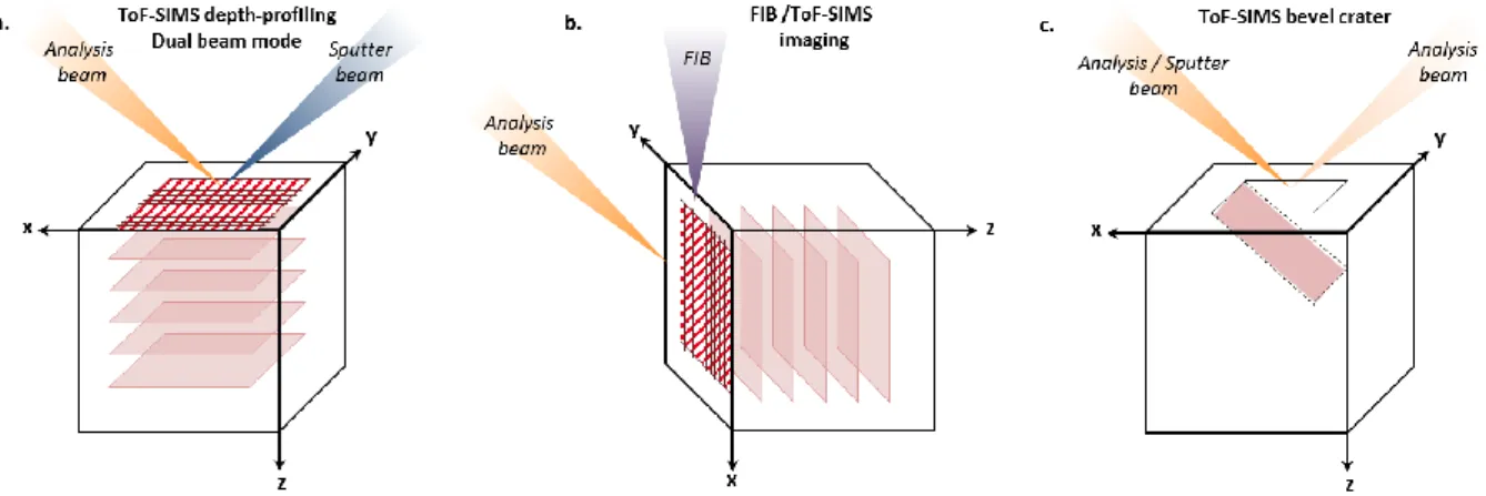
Besides the ToF-SIMS depth-profiling, the in-depth chemical information can be obtained by the FIB / ToF-SIMS imaging and the bevel crater approach (Figure II.2.b and c respectively).
Figure II.1 a. Schematic of the ToF-SIMS dual beam instrument. Information provided by the detected secondary ions: b. mass spectrum, c. chemical image for each ion and d. depth profile of secondary ion intensities.
Figure II.2 Schematic of the a. ToF-SIMS depth-profiling dual beam mode, b. FIB / ToF-SIMS imaging and c. ToF-SIMS bevel crater.
The FIB / ToF-SIMS approach is suitable to analyze the 2D planes perpendicular to the top of the sample surface, contrary to the depth-profiling where the analyzed 2D planes are the one parallel to the sample surface [77]. The third approach consists on creating a bevel crater
instead of a flat crater. The ion beam is used to mill the surface in a bevel shaped crater by varying the dose from 0 to 100% from one side of the crater to the other. This method allows a rapid surface study of the generated cross-section and is especially useful on thin multi-layers structures as the bevel introduces a magnification factor. [78]
The ToF-SIMS analysis beam scans areas from a few µm2 to several hundred of µm2 with a pixel resolution between 2 x 2 pixels and 2048 x 2048 pixels. From each pixel, a mass spectrum such as the one in Figure II.1.b is collected. From each scan, 2D images such as those shown in Figure II.1.c are produced. Moreover, from each 3D analysis the previous results are collected as a function of the sputter time (t). From them, a depth profile as shown in Figure II.1.d and a 3D visualization are generated.
- Mass spectrum: one mass spectrum is collected per pixel representing the number of detected secondary ions (intensity) as a function of their m/z ratio. Two important characteristics of the spectra are their mass resolution of up to M/ΔM > 104 and their mass range of 10 kDaltons which enables the detection of polymers, isotopes, ions, among others [70,79]. The pulsing width of the primary beam influences the mass resolution of the spectra; shorter the pulse is, higher is the mass resolution. However, this last one is also affected by other factors such as the dead time of the detector, the sample topography or roughness and the correction of the secondary ion energy distribution [70,74].
- 2D ToF-SIMS images: they are obtained by locating the secondary ion intensity of every m/z specie at the pixel from where it was sputtered. The lateral resolution can go down to 100 nm and it depends mainly on the interaction volume that is related to the diameter of the primary beam. The smaller this is, the higher is the lateral resolution
[70,80]. Aberrations of the 2D images are commonly found because the ToF-SIMS neglects the sample topography when performing an analysis. Concrete examples will be given in 0.
- Depth profile: it represents the intensity of each m/z specie as a function of the sample depth or sputter time. The ToF-SIMS may achieve a depth resolution down to 1 nm depending on the accumulation of the sputtering damage and the sample roughness. It is influenced by the sputter beam energy, current, angle, sample morphology, among others [81,82]. Information about its calculation can be found in [73,83,84].
- 3D visualization: it is generated by stacking the ToF-SIMS images. However, the aberrations in the ToF-SIMS images propagate themselves to the 3D visualization.
The third dimension of the volume corresponds to the sputter time. This can be transformed into a depth (z) scale using the sputter rate (SR) [nm/s], Eq. II.2.
𝑧[𝑛𝑚] = 𝑆𝑅. 𝑡 Eq. II.2 [73]
1.1.1. S
PUTTER RATE CALCULATIONThe sputter rate refers to the velocity at which the atoms are extracted from the sample. It changes vertically, in the depth-profile, and horizontally, from pixel to pixel, product of the damage accumulation on the sample surface and the non-homogeneous sputtering [69,85–87].
The sputter rate depends on the mechanism of energy transfer between the primary ions and the sample. Thus, its value relies upon the material nature, the sample topography and the setting of the primary beam. It can be calculated by [88]:
- depth-profiling a sample with well-known depth dimensions to determine the needed time to sputter a specific depth.
- measuring the depth of the crater created during the analysis with another technique and then use the Eq. II.2 to calculate the sputter rate.
- using the sputter yield (Sy) which is linked to the sputter rate (SR) by the relation of Eq. II.3. The equation includes the molar mass (M) of the material present in the sample, the primary ion beam current (I), the sample density (ρ), the Avogadro number (NA), the electron charge (e) and the surface area hit by the primary ions (A).
𝑆𝑅[𝑛𝑚/𝑠] = 𝑀. 𝐼. 𝑆𝑦
𝜌. 𝑁𝐴. 𝑒. 𝐴 Eq. II.3 [73]
The sputter yield is the number of secondary particles of a given specie (neutrals or charged) that were extracted from the surface per impact of primary ion. The sputter yield is affected by the sample topography, roughness and the analysis conditions. It is enhanced when the primary beam hits the surface at glancing angle [83] and it is directly proportional to the ion current, the primary energy and the mass of the primary ions. However, the opposite effect is seen when the mass of the primary ions is excessively increased or the beam energy is higher than 30 keV. In this case, there is a deep penetration of the primary ions producing their implantation at a large depth. Thus, collisions are not shallow enough to cause the ejection of atoms. [72,89] The theoretical values for the elements of the periodic table depending on the energy and angle of the primary beam can be calculated following the empirical formula developed by Yamamura et al. [90–92]. However, an experimental value can be obtained from Eq. II.4 where ρa is the atomic density, A is the surface area hit by the primary ions, z is the sputtered depth and Ip is the primary ion dose.
𝑆𝑦 =𝜌𝑎. 𝐴. 𝑧
𝐼𝑝 Eq. II.4 [72,74]
The ion dose corresponds to the number of primary ions per unit of area. It is calculated following the Eq. II.5 or the ToF-SIMS IONTOF software SurfaceLab 6.
𝐼𝑃[𝑖𝑜𝑛/𝑚2] = 𝐼. 𝑡
𝑒. 𝐴 Eq. II.5 [93]
1.2. I
ON-
SOLID INTERACTIONSThe collision of a primary ion accelerated to several keV with a surface is mainly led by elastic interactions between the primary ions and atoms from the surface. From the moment a primary ion strikes the surface, the energy from the ion is transferred to the sample. If the primary ion energy is higher than the surface bonding energy, the sputtering of atoms or molecules from the first 5 Å of the sample occurs. Sputtering-induced damages as dislocations, vacancies, stress, strain, atom implantation, recoil or cascade mixing are then produced in the following nanometers. After this damaged area, the maximum penetration of the primary ions is found. [69,84,94]
Three elastic collision models can explain this distribution in the sample [95,96]:
- Knock-on: two-body collision regime. The primary ion hits the surface; its energy is transferred to an atom of the sample. The atom has now enough energy to displace itself deeper in the sample or to be sputtered. This occurs for primary energy less than 1 keV. - Linear cascade: the energy transferred to the superficial atom is sufficiently high that it can collide with other atoms and transfer them enough energy for them to displace as well. Sputtering can occur if the cascade approaches the surface.
- Spike: the energy transferred to the atoms of the second collision causes them to collide with other atoms increasing the density of moving atoms. No sputtering is produced because the collisions are deep in the sample.
After the collision, low energy electrons, photons, neutrals and charged particles are emitted. These last one are the so-called secondary ions. They may be formed by, for example, the dissociation of MxOy and MxCsy compounds created after a reaction of remaining Cs+ or O2+ primary ions with M metallic atoms of the sample [72,97]. The oxygen keeps the negative charge as it is more electronegative and the M+ fragment is formed. In the opposite case, cesium can behave as an electron donor due to its low electronegativity creating fragments of Cs+ and M-.
This example relates the nature of the primary ion beam with the sputtering yield of a specific species [21,79,98]. The ionization theories vary depending on the nature of the matrix and differ in when and how the charges are created. At the moment there is not a formal explanation of the ionization process. However, it is possible to find some of the proposed models in the literature: nascent ion molecule model, desorption ionization model, the bond breaking model, electron tunneling model [21,94].
Along the entire process, the surface is constantly changing. The recoil implantation that corresponds to the displacement of one atom of the sample within the sample creates defects. The cascade produces layer mixing. The generated impurities, ion implantation, atomic mixing, surface roughness produce non-homogeneous sputtering, causing local changes in the sputtering yield and with it the diminution of the depth resolution. [96] This phenomenon of
local sputtering may also lead to the development of the surface topography, better-known as ion induced topography. The generated morphology usually starts with etch pits and it can evolved into ripples, pits, facets, etc. depending on the sputtering conditions and the sample nature [41,85,96,99].
1.3. T
IME-
OF-F
LIGHT MASS ANALYZERThe secondary ions are attracted to the analyzer using the voltage set by the extractor. Inside the 2 m flight tube, the ions are focused by a lens toward the detector. The ions reach the reflector (see Figure II.1.a) and their trajectory length is modified according to the ion energy. The higher the energy, the deeper the ion will enter into the reflector increasing his path before being redirected to the detector by an electrostatic field. Any extra energy that atoms from the same nature may have is compensated with a longer flight-path. Thus, ions of same nature will arrive at the same time to detector. The time-of-flight is calculated per secondary ion using the time spent between the pulsing of the analysis beam and its arrival to the detector. [21,70]
The number of detected secondary ions of species m, known as secondary ion intensity (Im), is calculated with the following relation:
𝐼𝑚 = 𝑛. 𝐼𝑝.𝑆𝑚. 𝑃𝑚+/−. 𝐶𝑚 Eq. II.6 [100]
The relation includes the surface concentration of the element m (Cm), the probability of that element to be ionized either positive or negative (Pm), the sputter yield of m particles (Sm), the primary ion dose (Ip) and the transmission efficiency of the instrument toward the detector (n), 90 – 95 % for the instrument we have used (ToF-SIMS V ION-TOF).
1.4. I
NSTRUMENTAL SETUP1.4.1. A
NALYSIS BEAMThe analysis beam is a low current (less than some pA) high energy pulsed beam. Generally, a liquid metal ion source (LMIS) is used. The beam can be formed by atomic ions or metal clusters: Bix+, Ga+, Aux+ and In+ are some of them. The bismuth is the most common due to the wide range of primary ion species that it produces (Bi+, Bi++, Bi
3+, Bi3++, Bi5+, Bi7+). A suitable analysis gun should produce the highest secondary emission with the smallest beam size. Empirically, it has been shown that the increase of projectile mass increases secondary ion emission. However, this trend can be reversed due to the lower velocity of heavier clusters as in the case of Bi5+. [84,93]
The ion source consists of two electrical contacts set on an insulating base. Those contacts are the support of a heater filament where a needle and a reservoir coated with the metal are mounted. A high negative potential is applied from an extractor located close to the tip of the needle. The needle is heated and due to the negative potential the electrons of the metal goes backwards while the positive metal ions move toward the tip creating a cone and starting the ion emission. [74,84,101]
The ions are accelerated to an energy that is typically between 15 keV and 30 keV. Electrostatic lenses focus the beam and a Wien filter (flight time filter) separates the ions by their mass. Electric and magnetic fields accelerate the atoms in order for them to be separated according to their velocity. Only the required type of ions goes through the filter to reach an aperture that gives final size of the beam. [96,101]
The mass resolution is defined by the pulse width, the shorter the pulse, the higher the mass resolution. However, a short pulse width reduces the secondary ion intensities and thus the signal-to-noise-ratio of the ToF-SIMS images. [79,93,102,103] Following these constraints,
diverse operation modes are possible:
- Bunched mode: suitable for high mass resolution analysis. It applies a pulse of about 600 ps with high current (more than 500 primary ions per pulse).
- Collimated mode: suitable for high lateral resolution analysis. The aperture defines the beam diameter, about 100 nm. Long pulse to guarantee a high signal-to-noise-ratio by increasing secondary ion intensity.
- Burst mode (patented by IONTOF): good compromise between the mass and the lateral resolution. The pulse time is about 1.5 ns with a current of 100 primary ions. Several pulse repetitions in one cycle are done in order to sum the secondary ion intensities obtained at each time. This way, the pulse is short enough to have 5000 M/ΔM mass
The analysis beam should sputter an insignificant depth compared to the entire sputtered depth, a fraction less than 0.01. To achieve this value, the dose ratio between sputter beam and analysis beam should be in the rage of 600 up to 1000 [45].
1.4.2. S
PUTTER BEAMThe sputter beam is used for 3D ToF-SIMS analysis. It is a DC, low energy (from 100 eV to a few keV), high current beam (up to several hundred nA). A high primary energy may fragment the molecules causing the loss of chemical information; a low primary energy (less than 500 eV) creates ion deposition and collision mixing on the surface. A compromise between fragmentation and depth resolution should be found.
C60+, SF5+, Arx+, O2+, Cs+, Xe+ are the most frequent ions for sputtering and they are used as atomic ions or as clusters. It is also possible, but not common, to use some of the primary ions on the list for analysis and sputtering. The selection of the sputter ions depends on the sample nature. The organic molecules are likely to be fragmented under a strong impact of the primary ions and then the chemical information can be missed [80]. Argon clusters sources
were developed to sputter polymeric matrices reducing the damage and fragmentation without losing secondary ion intensity. The energy of a single ion depends on the number of atoms in the cluster. Extensive information about ToF-SIMS analysis on organic materials can be found in those references[ [45,74,104,105].
The beam formation is different. The Cs+ ions are formed during the evaporation of a Cs metal or compound; the vapor flows towards a porous plug where it diffuses. They are then extracted and accelerated. On the other hand, the noble gas and oxygen beams are formed by electron impact ion sources. In this case, electrons are accelerated through an aperture where they collide with the gas molecules to produce the ions. References [21,74,96] give more information about this principle. The analysis area should be 9 times smaller and centered with the sputtered area to avoid the edge effects [45,79].
The chemical information provided by the ToF-SIMS characterization technique can be combined with other physical properties to obtain a better understanding of the sample.
2.
A
TOMIC FORCE MICROSCOPYThe atomic force microscopy (AFM) was created in 1986 by Binnig, Quate and Gerber [106]
to overcome the main limitation of the scanning tunnelling microscopy, the surface imaging of exclusively conductive samples. Its principle is based on the detection of interaction forces between the sample surface and a tip located a few nanometers above on a flexible cantilever. Those interaction forces are assumed to represent the surface topography.
2.1. G
ENERAL PRINCIPLEThe interaction forces between the tip and the sample surface vary with the tip-sample distance. Figure II.3 describes this variation and illustrates the three existing regimes: (i) no interaction force when the tip is far away from the surface, (ii) the attractive regime when the tip approaches itself toward the sample surface and, (iii) the repulsive regime when the tip is in contact with the sample. [107]
Different nature of forces are found within each regime. In the attractive regime, long and short-range forces in the range of pN to nN are detected [108]:
- Electrostatic force: long-range force produced by a non-zero potential difference between the tip and the sample. This force is always present for conductive or semi-conductive samples and tips.
- Magnetic force: long-range force obtained by the utilization of magnetic tips to locally measure magnetic properties of the sample.
- Van der Waals force: long-range force due to the variation in the local electric dipole between the atoms of the tip and the sample.
- Capillarity force: short-range force produced by the deposition of water molecules from the air in the sample or in the tip surface. A water meniscus between the sample and the tip is formed when they are close enough. This force can be reduced when working inside a glove box with controlled oxygen and H2O levels.
Figure II.3
Force – distance curve. Three regimes: attractive, repulsive and no forces. Three AFM operation modes are represented in the curve: the contact mode in the repulsive regime, the non-contact mode in the attractive regime and the intermittent-contact that includes the
The repulsive regime is dominated by the Pauli exclusion principle. It depends on the tip apex and the penetration of this one in the sample. The detected forces can be controlled by the cantilever geometry and nature, but in general, they have values of about 100 nN.
There is a different AFM operation mode associated to each regime. They are identified with different colours in the curve of Figure II.3:
- Contact mode: the tip is in contact with the sample while scanning. The analysis is consequently carried out in the repulsive regime (red part of the curve).
- Non-contact mode: the tip never touches the sample; it scans the surface in the attractive regime (blue part of the curve).
- Intermittent-contact mode: the tip traverses the attractive and repulsive regimes while scanning the sample (green part of the curve).
2.1.1. AFM
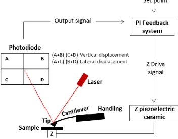
EXPERIMENTAL SETUPFigure II.4 shows the schematic of the AFM general principle used by all operation modes. A laser beam hits the end of the cantilever; its reflection reaches the center of a photodiode (0,0). The tip starts scanning the surface in the x-y plane, analyzing the number of points required by the user. Each point is called a pixel. The interaction force between the tip and the sample changes with the surface topography displacing the reflection of the laser at the photodiode. The photodiode determines the vertical displacement of the laser, called output signal, and sends it to the proportional-integral feedback system. This compares the detected value with a fixed set point. The set point corresponds to a property that allows to detect the modification of the interaction forces. It can be the amplitude or the frequency of the cantilever when this one is oscillating or the applied force when the tip is in contact with the surface.
Figure II.4
Schematic of the AFM principle and components: the four-quadrant photodiode to measure the cantilever deflection with the laser beam deviation, the feedback system which gives the z drive signal to the piezoelectric in order to restore the value to the set point.