Demonstration of a hitless bypass switch using nanomechanical
perturbation for high-bitrate transparent networks
The MIT Faculty has made this article openly available. Please share
how this access benefits you. Your story matters.
Citation
Chatterjee, Rohit, Mingbin Yu, Aaron Stein, Dim-Lee Kwong, Lionel
C. Kimerling, and Chee Wei Wong. “Demonstration of a hitless
bypass switch using nanomechanical perturbation for high-bitrate
transparent networks.” Optics Express 18, no. 3 (January 28, 2010):
3045. © 2010 OSA
As Published
http://dx.doi.org/10.1364/OE.18.003045
Publisher
Optical Society of America
Version
Final published version
Citable link
http://hdl.handle.net/1721.1/79709
Terms of Use
Article is made available in accordance with the publisher's
policy and may be subject to US copyright law. Please refer to the
publisher's site for terms of use.
Demonstration of a hitless bypass switch using
nanomechanical perturbation for high-bitrate
transparent networks
Rohit Chatterjee1, Mingbin Yu2, Aaron Stein3, Dim-Lee Kwong2, Lionel C. Kimerling4, and Chee Wei Wong1*
1Center for Integrated Science and Engineering, Solid-State Science and Engineering, and Mechanical Engineering,
Columbia University, New York, NY 10027, U.S.A.
2
The Institute of Microelectronics, Singapore 117685, Singapore
3Center for Functional Nanomaterials, Brookhaven National Laboratory, Upton, NY 11973, U.S.A. 4Microphotonics Center and Materials Processing Center, Department of Materials Science and Engineering,
Massachusetts Institute of Technology, MA 02139, U.S.A. *cww2104@columbia.edu
Abstract: We demonstrate an optical hitless bypass switch based on
nanomechanical proximity perturbation for high-bitrate transparent networks. Embedded in a single-level π-imbalanced Mach-Zehnder interferometer, the two nanomechanical-based ∆β-directional couplers permit broadband signal rerouting on-chip, while the selected wavelength remains unaffected at all times for optical filter reconfiguration. The optical hitless switch is implemented in the silicon nanophotonics platform, with experimental measurements matching well with numerical and theoretical modeling.
©2010 Optical Society of America
OCIS codes: (130.4815) Optical switching devices; (230.3120) Integrated optics devices
References and links
1. T. Barwicz, M. R. Watts, M. A. Popović, P. T. Rakich, L. Socci, F. X. Kärtner, E. P. Ippen, and H. I. Smith, “Polarization-transparent microphotonic devices in the strong confinement limit,” Nat. Photonics 1(1), 57–60 (2007).
2. F. Xia, L. Sekaric, and Y. Vlasov, “Ultracompact optical buffers on a silicon chip,” Nat. Photonics 1(1), 65–71 (2007).
3. B. G. Lee, A. Biberman, P. Dong, M. Lipson, and K. Bergman, “All-Optical Comb Switch for Multiwavelength Message Routing in Silicon Photonic Networks,” IEEE Photon. Technol. Lett. 20(10), 767–769 (2008). 4. B. G. Lee, X. Chen, A. Biberman, X. Liu, I.-W. Hsieh, C.-Y. Chou, J. I. Dadap, F. Xia, W. M. J. Green, L.
Sekaric, Y. A. Vlasov, R. M. Osgood, Jr., and K. Bergman, “Ultrahigh-Bandwidth Silicon Photonic Nanowire Waveguides for On-Chip Networks,” IEEE Photon. Technol. Lett. 20(6), 398–400 (2008).
5. M. Haurylau, G. Chen, H. Chen, J. Zhang, N. A. Nelson, D. H. Albonesi, E. G. Friedman, and P. M. Fauchet, “On-Chip Optical Interconnect Roadmap: Challenges and Critical Directions,” IEEE Sel. Top. Quantum Electron. 12(6), 1699–1705 (2006).
6. D. A. B. Miller, “Device Requirements for Optical Interconnects to Silicon Chips”, Proc. IEEE Special Issue on Silicon Photonics 97, 1166 – 1185 (2009).
7. Q. Xu, B. Schmidt, S. Pradhan, and M. Lipson, “Micrometre-scale silicon electro-optic modulator,” Nature 435(7040), 325–327 (2005).
8. C. K. Madsen, and J. H. Zhao, Optical Filter Design and Analysis: A Signal Processing Approach, John Wiley and Sons, Inc., New York, NY, USA, 1999.
9. B. E. Little, J. S. Foresi, G. Steinmeyer, E. R. Thoen, S. T. Chu, H. A. Haus, E. P. Ippen, L. C. Kimerling, and W. Greene, “Ultra-compact Si-SiO 2 microring resonator optical channel dropping filters,” IEEE Photon. Technol. Lett. 10(4), 549–551 (1998).
10. T. Barwicz, M. A. Popović, F. Gan, M. S. Dahlem, C. W. Holzwarth, P. T. Rakich, E. P. Ippen, F. X. Kartner, and H. I. Smith, “Reconfigurable silicon photonic circuits for telecommunication applications,” Proc. SPIE 6872, 68720Z – 68720Z–12 (2008).
11. H.-Y. Ng, M. R. Wang, D. Li, X. Wang, J. Martinez, R. R. Panepucci, and K. Pathak, “4×4 wavelength-reconfigurable photonic switch based on thermally tuned silicon microring resonators,” Opt. Eng. 47(4), 044601 (2008).
12. C. R. Doerr, L. W. Stulz, D. S. Levy, R. Pafchek, M. Cappuzzo, L. Gomez, A. Wong-Foy, E. Chen, E. Laskowski, G. Bogert, and G. Richards, “Wavelength add-drop node using silica waveguide integration,” J. Lightwave Technol. 22(12), 2755–2762 (2004).
13. V. Craciun, and O. W. W. Yang, “Ring resonator-based sparse reconfigurable optical add-drop multiplexer. part II: Node level analysis,” Proc. SPIE 5247, 561–568 (2003).
14. H. A. Haus, M. A. Popović, and M. R. Watts, “Broadband hitless bypass switch for integrated photonic circuits,” IEEE Photon. Technol. Lett. 18(10), 1137–1139 (2006).
15. M. A. Popović, H. A. Haus, and M. R. Watts, “General approach to hitless switching and FSR extension for resonators in integrated photonic circuits,” in Proc. of Optical Fiber Communication Conference, paper OWI66 (2006).
16. M. A. Popović, E. P. Ippen, and F. X. Kärtner, “Universally balanced photonic interferometers,” Opt. Lett. 31(18), 2713–2715 (2006).
17. M. A. Popović, T. Barwicz, F. Gan, M. S. Dahlem, C. W. Holzwarth, P. T. Rakich, H. I. Smith, E. P. Ippen, and F. X. Kärtner, “Transparent wavelength switching of resonant filters,” in Proc. of Conference on Lasers and
Electro-Optics, postdeadline paper CPDA2 (2007).
18. M. A. Popović, T. Barwicz, M. S. Dahlem, F. Gan, C. W. Holzwarth, P. T. Rakich, M. R. Watts, H. I. Smith, F. X. Kärtner, and E. P. Ippen, “Hitless reconfigurable and bandwidth-scalable silicon photonic circuits for telecom and interconnect applications,” in Proc. of Optical Fiber Communication Conference, paper OTuF4 (2008). 19. H. L. R. Lira, S. Manipatruni, and M. Lipson, “Broadband hitless silicon electro-optic switch for on-chip optical
networks,” Opt. Express 17(25), 22271–22280 (2009).
20. N. Sherwood-Droz, H. Wang, L. Chen, B. G. Lee, A. Biberman, K. Bergman, and M. Lipson, “Optical 4x4 hitless slicon router for optical networks-on-chip (NoC),” Opt. Express 16(20), 15915–15922 (2008).
21. R. E. Scotti, C. Madsen, C. H. Henry, G. Lenz, Y. P. Li, H. Presby, and A. White, “A hitless reconfigurable add-drop multiplexer for WDM networks utilizing planar waveguides, thermo-optic switches and uv-induced gratings,” in Proc. of Optical Fiber Communication Conference, 142 – 143 (1998).
22. P. T. Rakich, M. A. Popović, M. R. Watts, T. Barwicz, H. I. Smith, and E. P. Ippen, “Ultrawide tuning of photonic microcavities via evanescent field perturbation,” Opt. Lett. 31(9), 1241–1243 (2006).
23. M. Li, W. Pernice, and H. Tang, “Tunable bipolar optical interactions between guided lightwaves,” Nat. Photonics 3(8), 464–468 (2009).
24. M. Eichenfield, R. Camacho, J. Chan, K. J. Vahala, and O. Painter, “A picogram- and nanometre-scale photonic-crystal optomechanical cavity,” Nature 459(7246), 550–555 (2009).
25. G. S. Wiederhecker, L. Chen, A. Gondarenko, and M. Lipson, “Controlling photonic structures using optical forces,” Nature 462(7273), 633–636 (2009).
26. H. Kogelnik, and R. Schmidt, “Switched directional couplers with alternating ∆β,” IEEE J. Quantum Electron. 12(7), 396–401 (1976).
27. M. Papuchon, Y. Combemale, X. Mathieu, D. Ostrowsky, L. Reiber, A. Roy, B. Sejourne, and M. Werner, “Electrically switched optical directional coupler: Cobra,” IEEE J. Quantum Electron. 11(9), 921–922 (1975). 28. H. F. Taylor, “Optical switching and modulation in parallel dielectric waveguides,” J. Appl. Phys. 44(7), 3257–
3262 (1973).
29. H. A. Haus, Waves and Fields in optoelectronics, (Prentice Hall, 1984).
30. A. Yariv, “Coupled-wave theory for guided-wave optics,” IEEE J. Quantum Electron. 9(9), 919–933 (1973). 31. R. L. Espinola, M. C. Tsai, J. T. Yardley, and R. M. Osgood, Jr., “Fast and low-power thermooptic switch on
thin silicon-on-insulator,” IEEE Photon. Technol. Lett. 15(10), 1366–1368 (2003).
32. Q. Lai, W. Hunziker, and H. Melchior, “Low-power compact 2×2 thermooptic silica-on-silicon waveguide switch with fast response,” IEEE Photon. Technol. Lett. 10(5), 681–683 (1998).
33. R. S. Jacobsen, K. N. Andersen, P. I. Borel, J. Fage-Pedersen, L. H. Frandsen, O. Hansen, M. Kristensen, A. V. Lavrinenko, G. Moulin, H. Ou, C. Peucheret, B. Zsigri, and A. Bjarklev, “Strained silicon as a new electro-optic material,” Nature 441(7090), 199–202 (2006).
34. R. Soref, and B. Bennett, “Electrooptical effects in silicon,” IEEE J. Quantum Electron. 23(1), 123–129 (1987). 35. M.-C. M. Lee, and M. C. Wu, “Tunable coupling regimes of silicon microdisk resonators using MEMS
actuators,” Opt. Express 14(11), 4703–4712 (2006).
36. M. W. Pruessner, K. Amarnath, M. Datta, D. P. Kelly, S. Kanakaraju, P.-T. Ho, and R. Ghodssi, “InP-based optical waveguide MEMS switches with evanescent coupling mechanism,” J. Microelectromech. Syst. 14(5), 1070–1081 (2005).
37. E. Ollier, “Optical MEMS devices based on moving waveguides,” IEEE J. Sel. Top. Quantum Electron. 8(1), 155–162 (2002).
38. T. Bakke, C. P. Tigges, J. J. Lean, C. T. Sullivan, and O. B. Spahn, “Planar microoptomechanical waveguide switches,” IEEE J. Sel. Top. Quantum Electron. 8(1), 64–72 (2002).
39. A. Taflove, and S. C. Hagness, Computational Electrodynamics: The Finite-Difference Time-Domain Method, Third Edition. Artech House Publishers, 2005.
40. Y.-I. Lee, K.-H. Park, J. Lee, C.-S. Lee, H.-J. Yoo, C.-J. Kim, and Y.-S. Yoon, “Dry release for surface micromachining with HF vapor-phase etching,” J. Microelectromech. Syst. 6(3), 226–233 (1997). 41. M. Offenberg, B. Elsner, and F. Lärmer, “Vapor HF etching for sacrificial oxide removal in surface
micromachining,” Electrochemical Society Fall Meet 94, 1056–1057 (1994).
42. C. R. Helms, and B. E. Deal, “Mechanisms of the HF/H2O vapor phase etching of SiO2,” J. Vac. Sci. Technol.
10(4), 806–811 (1992).
43. P. J. Holmes, and J. E. Snell, “Vapour etching technique for photolithography of silicon dioxide,” Microelectron. Reliab. 5(4), 337–341 (1966).
1. Introduction
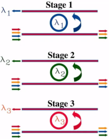
In current wavelength division multiplexing (WDM) systems and photonic on-chip interconnect networks [1–6], rerouting of wavelength signals is a critical element to optical information processing. This can be achieved with reconfigurable optical add/drop multiplexers (OADMs) [7–9]. The present challenge involving such OADMs is that their reconfiguration to reroute a different wavelength must take a finite time [10–13], which is typically in the range of microseconds to even milliseconds. During this reconfiguration time, undesired wavelengths get rerouted if they are in the same channel as the OADMs. This is further illustrated in Fig. 1. For example, for a 40 Gbit/s channel, a 1 microsecond
reconfiguration time of the OADMs results in 4 × 104 bits lost when the targeted wavelength
is tuned from one position to the next or when the filter is switched on or off in an optical network. Our objective is therefore to demonstrate a design that permits wavelength filter reconfigurability and on/off switching without any loss of information bits. Also, the entire operation needs to be performed without affecting other wavelength channels – in other words, the operation needs to be transparent or hitless [14]. Two main requirements emerge from this scenario: (1) enabling a binary on/off switching of the filters without any loss of data bits, and (2) enabling filter reconfigurability without any loss of data bits by temporary transfer of data from the signal bus to a ``bypass” bus without disturbing other wavelength channels. Secondary objectives are to achieve small form factors and low power requirements for scalability to high-density integrated optics, materials compatibility with silicon photonics for potential processing integration, and minimal design and fabrication complexity in order to for high-density scalability.
Fig. 1. A challenging problem in current WDM networks. The flow of signals through a reconfigurable optical add-drop multiplexer (OADM) before, during and after reconfiguration is shown schematically. The different wavelength signals are depicted by different colored arrows. Stage 1 depicts the situation before any tuning of the OADM has taken place. The desired wavelength signal λ1 is dropped out and re-routed. Now, if it is desired to drop λ3 instead of λ1, reconfiguration of the OADM takes place. During this finite time, the OADM is tuned through all wavelength channels in between λ1 and λ3 and undesired wavelength signals get re-routed. As an example, in Stage 2 at some time step during reconfiguration, λ2 (where λ1 < λ2 < λ3) although not desired, gets re-routed to a different channel.
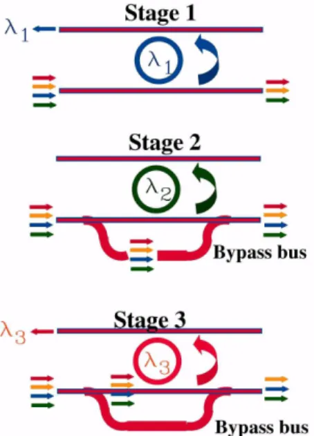
Recently a few solutions to this approach of hitless tuning has been suggested [14–19], along with spatial non-blocking switches [20] and earlier studies [21]. The approach towards solving this important problem described in Ref. 14 to 18 employs a “slow” hitless switching scheme for lossless reconfiguration. Here we demonstrate experimentally, for the first time, this hitless switch scheme using integrated nanomechanical proximity perturbation in a single-level π-imbalanced Mach-Zehnder interferometer.
The operation of the hitless bypass switch is described schematically in Fig. 2, and a practical implementation of this scheme is illustrated in Fig. 3. It consists of two inverse-signed symmetrically actuated 2 × 2 switches arranged in a balanced Mach Zehnder configuration. In this implementation, the 2 × 2 switch is a ∆β switched directional coupler (where ∆β is the propagation constant mismatch between two waveguides) with nanomechanical proximity perturbation [22–25] to control the power transfer ratios [26–28]
with tuned propagation constant mismatch ∆β. A φ-phase shift, relative to the phase response
of the reconfigurable filter, is introduced to one arm of the Mach Zehnder, with a π-phase shift desired if no reconfigurable optical device is present. The switch does not need to be fast as it serves as a bypass router for the reconfigurable filter.
Fig. 2. The hitless bypass switch - a possible solution to WDM reconfiguration. The hitless bypass switch schematically described here attempts to provide a possible solution to the problem described in Fig. 1. Similar to Fig. 1, the flow of signals through a reconfigurable optical add-drop multiplexer (OADM) before, during and after reconfiguration is shown schematically. The different wavelength signals are once again depicted by different colored arrows. Stage 1 depicts the situation before any tuning of the OADM has taken place. The desired wavelength signal λ1 is dropped out and re-routed. Now as described in Fig. 1, if it is desired to drop λ3 instead of λ1, reconfiguration of the OADM takes place. During this finite time, the OADM is tuned through all wavelength channels in between λ1 and λ3. To prevent undesired wavelength signal loss, during the reconfiguration of the OADM, the hitless bypass switch provides a path where all the signals are temporarily transferred, thus completely bypassing it. This is shown in Stage 2. In Stage 3, after reconfiguration of the OADM is complete, the hitless bypass switch allows all wavelength signals to remain in the original channel and the desired wavelength λ3 gets re-routed.
2. Hitless bypass switch operation
The operation of the hitless bypass switch is described in Ref. 14, and illustrated here in Fig. 4 for convenience. The directional couplers are designed such that in the unperturbed case (∆β = 0) complete power transfer takes place from one waveguide to the other.
Fig. 3. Practical implementation of the hitless bypass switch. Schematic of a practical implementation of the hitless bypass switch using nanomechanical proximity perturbation based ∆β directional coupler switches is shown. Three main functional characteristics needed in this design are depicted: (1) cascading of two perturbed directional couplers in a Mach-Zehnder configuration, (2) large-amplitude perturbation of the directional couplers, and (3) inclusion of a φ-phase shift in one of the interferometer arms.
Case I: (∆β ≠ 0) In the off-state, the ∆β switches are completely detuned (Fig. 4a) and all
input wavelengths from the top port (a1 in Fig. 4a) go through the top port a3 of the directional couplers to the wavelength selective device, which in this case is a ring resonator filter. The desired wavelength then gets rerouted while the other wavelength channels remain unaffected and emerge out of a5.
Case II: (∆β = 0) During reconfiguration of the ring resonator filter, the switches are
synchronously turned to the on-state (unperturbed case; Fig. 4b) and all input wavelengths travel from the top input port (a1 in Fig. 4b) to port a4 and are then transferred back to a5. Thus, the switch creates a bypass port for the wavelengths during the tuning of the OADM.
It is important to note that during all intermediate states between the unperturbed case and completely detuned case or vice versa, the undesired wavelength channels remain unaffected
and always exits out of the port a5. This is achieved because of the reversal of the input of the
second directional coupler with respect to the first, and also by the π-phase shifter which causes destructive interference of the signals at the bottom port port a6 of the second directional coupler. As an example, we illustrate the 3-dB scenario in Fig. 4c. In the 3-dB
coupler, the signal input a1 power is evenly split between two arms, with a π/2 phase lag in
(for example) the bottom arm. The signal in the bottom arm is then additionally phase-lagged by π. Upon exit of the second cascaded perturbed directional coupler, the wave in a6 is
destructively interfered, while the wave in a5 maintains unchanged in this transition state. In
all other transition states, we emphasize that this analysis continues to holds true, as with the 3-dB transition state. This will be further verified with coupled-mode calculations in the next section. The resultant signal intensities for various states are summarized in Table 1, with α
the signal intensity in port a3. For any phase shifts introduced by optical devices in the bypass
Fig. 4. Schematic of signal propagation through the hitless bypass switch. a, for limiting condition of completed detuned state. b, for limiting condition of completely unperturbed state. c, for the 3-dB transition state. Notice in the 3-dB transition state, the power in the top arm is π-phase shifted, leading to destructive interference at the exit of the perturbed directional coupler. This maintains power in a5 throughout the transition.
Table 1. Resulting signal intensities for various states.
Detuning state Bypass region signal a3 (normalized to a1(0))
Bypass region signal a4 (normalized to a1(0))
Bypass region signal a5 (normalized to a1(0))
Unperturbed state 0 1 1
Completely detuned state 1 0 1
3-dB transition state 0.5 0.5 1
All other transition states varies, α varies, 1-α 1
As described in Ref. 14, the coupled mode theory formalism [29,30] has been employed to illustrate the operation and performance sensitivity of the hitless switch in the weakly coupled regime. The net transfer matrix for the two cascaded directional couplers and the phase shifter, phase-shifted by ± ∆θ/2, is described in Ref. 14 as:
( ' / 2) / 2 11 ' ' j j T rr e− φ φ+ + ∆θ tt e∆θ = − (1)
(
( / 2) ( ' / 2))
21 ' ' j j T = −j t re− φ+ ∆θ −tr e φ+ ∆θ (2)where r (r’), t (t’) and φ (φ’) are the reflection, transmission and phase of the first (second)
directional coupler. As defined in Ref. 14, the transmitted wave amplitudes b'
'
b =T a, with T12= −T21*,
* 22 11
T = −T . If we assume that we have identical ∆β switches under
synchronous operation, then r = r' and t = t'. To achieve complete transmission, Eqs. (1) and (2) verifies that two conditions need to be true: (1) switch 2 input has to be reversed with respect to switch 1 so that φ = -φ' and, (2) ∆θ = π or a π differential phase shift must be introduced to one of the arms of the directional coupler [14].
3. Performance and sensitivity analysis of the design
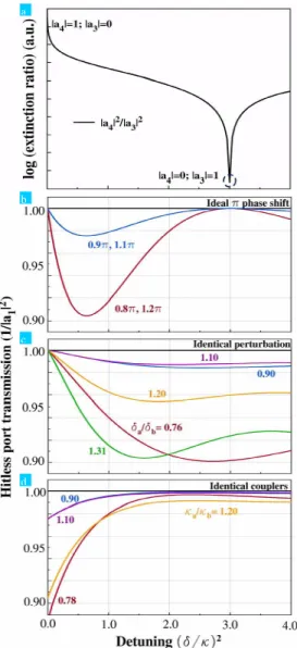
Figure 5a illustrates the results of coupled-mode analysis on the two cascaded perturbed directional couplers in the Mach-Zehnder configuration. The extinction ratio, defined as
2 4
a /a32, is illustrated for various
(
)
2
/
δ κ ratios, where δ ≡(β1−β2) / 2 is the propagation
constant mismatch (detuning) between the two waveguides (β1 and β2), and κ is the
coupling strength. With zero detuning, all power is found in a4; as the detuning δ goes up to
3κ, the signal in a4 drops to zero and all the power goes to a3. We note that this transfer does not affect the power levels in a5 and a6 during the bypass switching operation. Unity output power ( a5 2; Port 5) is always observed for all intermediate states (expressed by varying
(
δ κ/)
2 ratios), confirming the hitless nature of the designed switch. The sharp dip in the extinction ratio as δ gets close to 3κalso suggests that the detuning needs only to get close to optimal design values and a sharp dip in transmission of a42 can be observed inexperiment. Alternatively, this suggests that even if there are device nanofabrication variations from the optimal design parameters, a sharp dip will still be observable in experiments, since the range of δ is sufficiently large - using ∆β perturbation - to compensate for deviations of κ from design.
Variations on the symmetry of the ∆β perturbation and coupling, and π-imbalanced Mach-Zehnder are investigated through closed-form solutions from coupled-mode theory. Figure 5b
shows the power in the hitless port a52 (normalized by input power
2 1
a ) as the device goes
through the transition states, when the π-phase shift departs from ideal. In particular, we observe an excess loss of ~0.1 dB (0.4 dB) for a 10% (20%) variation in the desired π-phase
shift. During the bypass switch transition, the maximum excess loss occurs when δ/κ = 3 /2.
Furthermore, as shown in Fig. 5b, we emphasize that the switch remains hitless with zero
excess loss for all phase variations when δ/κ = 3 . This is due to zero cross-over when the
perturbed directional couplers are completely detuned.
Figure 5c shows hitless port a52as the device goes through the transition states, when the
two perturbed directional couplers departs from ideal. In particular, to keep the excess losses
below 0.5 dB, variations in the perturbations of the two directional couplers (δa/δb) should be
kept between 0.76 and 1.31 of each other. In addition, unlike the variations on the π-phase shift analyzed in Fig. 6a, there are residual transmission losses even at δ/κ = 3 due to incomplete field interference when the perturbations are asymmetric. Figure 5d shows the sensitivity of the two-cascade perturbed directional coupler design to asymmetry in two couplers, which may arise from nanofabrication variations in the directional coupler gap separation. To keep the excess losses below 0.5 dB, variations in the coupling coefficients of the two directional couplers (κa /κb) should be kept between 0.78 and 1.20 of each other. Residual transmission losses are also due to incomplete field interference when the couplers are asymmetric.
a
b
c
d
Fig. 5. Closed formed solution using coupled mode theory. a, Power in ports a3 and a4 for different detunings. When δ/κ = 3, all power from a4 gets transferred to a3 and complete detuned case is achieved. Note that for all values of the detuning parameter, the transmission in the hitless port is always 100% irrespective of the states of the directional coupler. (b, c, d), Sensitivity analysis of the two-cascade directional coupler design due to variations in π-phase shift (b), asymmetric perturbation (c) and coupling coefficients (d). Variations are investigated for a design threshold loss of 0.5 dB.
4. Nanomechanical proximity perturbation based ∆β directional coupler switch
A key component of the hitless bypass switch is the ∆β directional coupler, where the propagation mismatch can be controlled through thermal heating [31,32], electro-optic tuning [33,34], or suspended movable waveguides [35–38]. The first two approaches require relatively high powers, while with an electrostatic approach for the movable waveguides, significantly lower power switching is required. Here we employ electrostatic actuation of a fabricated movable dielectric nanobeam (100 nm in width and 200 nm in height, as shown in the inset of Fig. 6b) for proximity perturbation of the directional coupler.
Fig. 6. Numerical calculation of detuning parameter (δ/κ) for a high index contrast system. a, 3D FDTD method was used to find the coupling length for various separations between the two arms of the directional coupler. Here coupling length refers to the length required for complete coupling of light from one port of the directional coupler to the other. For a particular separation, the length is found and then κ is calculated. The inset gives the geometry and dimensions of the directional coupler used in the simulation. Inset also gives the 3D FDTD calculation showing the transfer of power from one port to the other looking from the top of the directional coupler. b, The detuning parameter (δ/κ) is plotted against the proximity distance. The figure shows that the required detuning parameter value (δ/κ = 3) can easily be achieved using the proximity perturbation method. Inset shows the geometry and dimension of the device that was studied.
As shown in Fig. 6a, our particular implementation is for a silicon-based directional coupler, with each (500 nm × 200 nm) waveguide designed to support a single transverse electric (TE) mode. 3D finite-difference time-domain simulations [39] were performed to
obtain the coupling lengths versus the separation distances (for example, a κ of ~1.85 × 10⁴
m−1 for a gap separation of 280 nm). We then examined numerically the perturbed waveguide
propagation constant β’ in the first waveguide, for varying proximity distance d (labeled in the
inset of Fig. 6b) of the nanobeam from the directional coupler. δ was obtained from (β’ - β2)/2
where β2 is unperturbed propagation constant of the second waveguide. Figure 6b shows the
resulting designed δ/κ values for varying nanobeam proximity distance d. A large set of δ/κ values can be obtained within the controllable range of d. Particularly, we note that the desired detuning δ/κ of 3 can now be achieved for complete switching, as required in the hitless switch.
Fig. 7. 3D numerical simulations of the influence of the perturbing dielectric on the high index contrast directional coupler system. a, Cross-section view of the directional coupler system showing the E-field distribution for different perturbing distances. As the perturbing distance is increased from panel (1) to panel (3), the mode shifts from the launch arm to the other arm of the directional coupler representing the unperturbed state of operation of the switch. b, Top: FDTD results showing unperturbed cross state. Bottom: FDTD results showing completely detuned state, with the power remaining in the source waveguide at the output plane.
We further confirm the switching with finite-difference time-domain results as shown in Fig. 7, for perturbed directional coupler with a 85 um coupling length. The top panel of Fig. 7b shows the directional coupler without any perturbation [see also Fig. 7a(3)]; the bottom panel shows the completely detuned state, with power remaining in the source waveguide at the output [see also Fig. 7a(1)]. In the completely detuned state (Fig. 7b bottom panel), we also note the weak spatially-oscillating fields between the two waveguides, which correlates with earlier suggestions from coupled mode theory, with an estimated maximum power transfer of 0.25 at half the original coupling length.
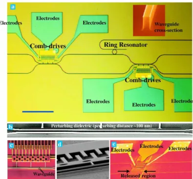
5. Nanofabrication of the hitless bypass switch
Encouraged by the numerical and theoretical simulations, we fabricated the complete hitless bypass switch on silicon-on-insulator wafers with 200 nm silicon device thickness and 3000 nm oxide substrate. The devices are patterned using deep-UV or electron-beam lithography, with reactive ion etching as shown in Fig. 8a to 8e. The two ∆β directional couplers are cascaded in the Mach Zehnder arrangement, with the π-phase shift is implemented with extension of one of the Mach-Zehnder arms by half its guided wavelength. The directional coupler gap is 250 nm. To demonstrate the hitless switch operation, the coupling lengths are chosen to be 40 um. This ensures a complete cross state when unperturbed (with 0.4-dB excess loss) and a mixed cross / bar state (74.6% power in cross state, 16.5% in bar state, with remaining in excess loss) when perturbed with 90 nm proximity distance.
d
Fig. 8. Fabrication results of the hitless bypass switch. a, Optical microscope image of the hitless bypass switch with the cascaded nanomechanical proximity perturbation based directional coupler ∆β switches and a ring resonator coupled to one of the arms of the Mach Zehnder interferometer. Scale bar: 100 µm. Inset shows the cross-section profile of a waveguide (not same device) with vertical sidewalls and small sidewall roughness. b, Close-up SEM image of the perturbing dielectric and the waveguides. Perturbing distances of ~90 to 100 nm was achieved for some of the devices. c, SEM image of the comb-drive actuators. The perturbing dielectric is connected to the comb-drives through thin beams. d, Optical microscope image of the mask created from photoresist. The clear area is directly exposed to the vapor HF and the oxide underneath that gets taken away releasing the comb-drives and the directional coupler. e, SEM image of a ∆β switch after vapor HF and oxygen plasma to remove the photoresist layer.
Almost vertical sidewalls with very little sidewall roughness (less than 5 nm) were achieved. Overall, less than 6% deviation from the designed dimensions were obtained in the hitless switch nanofabrication, within the tolerance levels for less than 0.5 dB excess loss targets. Gold electrodes were next patterned onto the silicon-on-insulator samples through electron-beam lithography and thermal evaporation. A photoresist mask is then patterned and the oxide underneath the device region undercut with vapor hydrofluoric acid [40–43] to suspend the perturbed directional couplers and the comb-drive actuators for measurements.
6. Experimental results and discussions
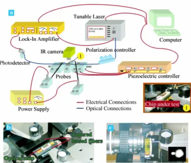
The fabricated devices were tested using a tapered lensed fiber-chip-fiber transmission setup (Fig. 9), consisting of a tunable laser (1480 nm to 1580 nm) as the input source with lock-in
amplification, polarization controllers and precision xyz-stages for input/output fiber
positioning to the waveguides. To actuate the nanomechanical beams and the comb-drives, four external probes were connected to the electrodes (two for each ∆β directional coupler switch) with static DC differential bias applied during the optical measurements.
Fig. 9. Experimental setup for testing the performance of the hitless bypass switch. a, Schematic of the experimental setup. Inset shows a close up image of the chip under test together with the input and output tapered lensed fibers and two electrical probes. To measure the hitless bypass switch four probes was used. b, Zoomed in top view photograph of the chip without the probes. c, Modified setup to collect the output light using an objective lens instead of the tapered lensed fiber. Inset shows the output IR image seen from the cross-section of the waveguide ends. It shows that the output light from one of the arms of the bypass switch is much stronger than the output from the other arm.
We first measure directly the switching contrast of the nanomechanical proximity perturbation based ∆β directional coupler switches. The drop port transmission of the ring resonator (coupled to one of the arms of the Mach Zehnder interferometer) was measured, in both the perturbed (0V DC bias) and unperturbed states. To achieve the unperturbed state, a 40V DC bias was applied to the electrodes of the comb-drive actuators to pull the nanomechanical dielectric beam away from the directional couplers. The result of the experiment is presented in Fig. 10c. Almost 31 dB of switching contrast was achieved at the resonance peak wavelength of 1540 nm. The variation in the peak transmission is suspected to be due to wavelength-dependences of the coupler. The high extinction ratio is achieved because of the small proximity perturbation distance (~90 nm) obtained for the nanofabricated devices. Figure 10b shows the topview infrared images of the chip collected in the far-field, corresponding directly with the input and output port positions of Fig. 10a.
1490 1500 1510 1520 1530 1540 1550 1560 1570 1580 -2 -1 1500 1520 1540 1560 1580 T ra n s m is s io n Wavelength (nm) Wavelength (nm) T ra n s m is s io n 1500 1520 1540 1560 1580 0 dB -10 dB -20 dB port B (40 V) port B (0 V) port C (40 V) port C (0 V) perturbed (0V) unperturbed (40V) 0.000 0.010 0.012
Fig. 10. Measurement results on the hitless bypass switch. a, Light-path in the switch for the perturbed (top figure) and unperturbed cases (bottom figure). Note that, in both cases, light always emerges out of port B and no light comes out of port C. The perturbed case is chosen such that there is light-path in both arms of the Mach-Zehnder to specifically illustrate the hitless switch operation. b, Top-view infrared image of the hitless bypass switch in both example states. c, Transmission spectrum (linear scale) from the drop port of the ring resonator in the perturbed and unperturbed cases. With the perturbed state (0V bias), light on-resonance with the microring resonator on the top interferometer arm is filtered into the drop port, with the resulting spectral resonances. At 40V, the unperturbed condition is achieved and almost all light goes through the bottom portion of the switch and negligible amount of light gets dropped through the ring resonator. 31 dB of contrast is achieved between the perturbed and unperturbed states. d, Transmission measurements through port B and C of the hitless bypass switch for the perturbed and unperturbed cases. An averaged extinction ratio of 17.3-dB and 11.8-dB is achieved for the unperturbed and perturbed cases respectively, across the wavelength range demonstrated.
To verify the hitless performance of the bypass switch, the transmission through port B and port C (illustrate in Fig. 10a) was measured for the two example unperturbed (40V) and perturbed (0V) cases. The result is shown in Fig. 10d. From the results, it is clear that the measured transmission through port C always has suppressed transmission for our perturbed and unperturbed states, for the full range of wavelengths examined with our tunable laser source. Note that the perturbed case has light intensity in both arms of the π-imbalanced Mach-Zehnder (74.6% power in cross state and 16.5% in bar state). With the π-phase shift, the fields destructively interference in the second directional coupler, with output transmission in port C suppressed. Moreover, the transmission through port B is always high for the non-resonant wavelengths irrespective of the state of the individual ∆β switches, demonstrating the functional performance of the bypass switch. We also note that in port B there are local resonances (dips in the dash-dot green plot) during the perturbed (0V) state, which arises from the finite reflections at the interfaces of the ∆β switches and can be reduced through adiabatic tapering at the interfaces. We emphasize that the average extinction ratio (between port B and C) preserves an approximately 17.3-dB and 11.8-dB intensity contrast
for the unperturbed and perturbed states, across the wavelength range demonstrated for the hitless switch.
7. Conclusion
We present the first implementation of a nanoelectromechanical single-level hitless bypass switch, in a silicon photonics platform. The proximity perturbation method was introduced to demonstrate the cross-to-bar state switching in each of the two cascaded ∆β switches in the Mach-Zehnder interferometer. With an included microring filter, an almost 31 dB of extinction ratio with negligible undesired wavelength rerouting was demonstrated. This allows an optical hitless switch for future high density integrated circuits. Future studies include high bitrate measurements to demonstrate the implementation of this hitless switch in on-chip nanophotonic networks for optical signal processing.
Acknowledgement
This work is dedicated to Professor Herman Haus, who originated the configuration of this hitless switch. We acknowledge stimulating discussions with M. Popovic, M. Watts, X. Yang, S. Kocaman, M. Aras, A. Biberman, K. Bergman, and M. Beals; generous use of the vapor HF system with J. Hone and M. Klima; use of probes from K. Shepard; and partial funding from the DARPA MTO Electronics and Photonics Integrated Circuits program.