Publisher’s version / Version de l'éditeur:
Vous avez des questions? Nous pouvons vous aider. Pour communiquer directement avec un auteur, consultez la première page de la revue dans laquelle son article a été publié afin de trouver ses coordonnées. Si vous n’arrivez pas à les repérer, communiquez avec nous à [email protected].
Questions? Contact the NRC Publications Archive team at
[email protected]. If you wish to email the authors directly, please see the first page of the publication for their contact information.
https://publications-cnrc.canada.ca/fra/droits
L’accès à ce site Web et l’utilisation de son contenu sont assujettis aux conditions présentées dans le site LISEZ CES CONDITIONS ATTENTIVEMENT AVANT D’UTILISER CE SITE WEB.
Nanotechnology, 30, 23, pp. 1-17, 2019-03-25
READ THESE TERMS AND CONDITIONS CAREFULLY BEFORE USING THIS WEBSITE. https://nrc-publications.canada.ca/eng/copyright
NRC Publications Archive Record / Notice des Archives des publications du CNRC :
https://nrc-publications.canada.ca/eng/view/object/?id=e0ccd675-a940-44af-8c7e-510a04f66d6c
https://publications-cnrc.canada.ca/fra/voir/objet/?id=e0ccd675-a940-44af-8c7e-510a04f66d6c
NRC Publications Archive
Archives des publications du CNRC
This publication could be one of several versions: author’s original, accepted manuscript or the publisher’s version. / La version de cette publication peut être l’une des suivantes : la version prépublication de l’auteur, la version acceptée du manuscrit ou la version de l’éditeur.
For the publisher’s version, please access the DOI link below./ Pour consulter la version de l’éditeur, utilisez le lien DOI ci-dessous.
https://doi.org/10.1088/1361-6528/ab0393
Access and use of this website and the material on it are subject to the Terms and Conditions set forth at
Nanowire-based sources of non-classical light
Nanotechnology
TOPICAL REVIEW • OPEN ACCESS
Nanowire-based sources of non-classical light
To cite this article: Dan Dalacu et al 2019 Nanotechnology 30 232001
View the article online for updates and enhancements.
Recent citations
Demonstration of InP/InAsP/InP axial heterostructure nanowire array vertical LEDs
Tomoya Akamatsu et al
-Review on the quantum emitters in two-dimensional materials
Shuliang Ren et al
-Topical Review
Nanowire-based sources of non-classical
light
Dan Dalacu , Philip J Poole and Robin L Williams
National Research Council of Canada, Ottawa, Ontario, K1A 0R6, Canada
E-mail:[email protected]
Received 5 November 2018, revised 19 December 2018 Accepted for publication 31 January 2019
Published 25 March 2019
Abstract
Sources of quantum light that utilize photonic nanowire designs have emerged as potential candidates for high efficiency non-classical light generation in quantum information processing. In this review we cover the different platforms used to produce nanowire-based sources, highlighting the importance of waveguide design and material properties in achieving optimal performance. The limitations of the sources are identified and routes to optimization are proposed. State-of-the-art nanowire sources are compared to other solid-state quantum emitter platforms with regard to the key metrics of single photon purity, indistinguishability and entangled-pairfidelity to maximally entangled Bell states. We also discuss the unique ability of the nanowire platform to incorporate multiple emitters in the same optical mode and consider potential applications. Finally, routes to on-chip integration are discussed and the challenges facing the development of a nanowire-based scalable architecture are presented.
Keywords: single photon sources, quantum dots, semiconductor nanowires (Some figures may appear in colour only in the online journal)
1. Introduction
Non-classical light plays a major role in many quantum information technologies [1]. Light sources that produce
single photons or entangled photon pairs are a required resource in many quantum-secured communication and quantum computing schemes. Sources based on solid-state emitters have emerged as a promising scalable solution for the generation of non-classical light and the advances in thisfield over the last half decade have been the subject of numerous review articles[2–10].
Depending on the application, an ideal non-classical source would generate single photons or entangled photon pairs on-demand at high repetition rates with unity efficiency. For many schemes, the sequential single photons emitted by
the source are required to be indistinguishable from each other, as well as indistinguishable from photons emitted by remote sources. Such sources have proven difficult to man-ufacture in the solid state: there is typically no control of the emitter position, making it difficult to isolate single emitters as required to ensure high single photon purity. Spectral diffusion due to a fluctuating charge environment [11] and
interaction with the phonon bath[12] lead to spectra that are
not Fourier-transform limited, reducing indistinguishability. For the case of quantum dots(QDs), which offer a mechanism to produce polarization entangled pairs via the biexciton– exciton cascade [13], the phase term between the
polariza-tions of the emitted pair due to system asymmetries makes it difficult to harness the entanglement [14]. Finally, for emitters
in bulk, device efficiencies are extremely low due to the difficulty in extracting light from high index materials [15].
These limitations have, to a large extent, been mitigated by employing optical microcavities [16, 17] in conjunction
with resonant excitation [18–20]. By coupling the emitter to
an optical mode that is easily collected, high efficiency
Nanotechnology 30(2019) 232001 (17pp) https://doi.org/10.1088/1361-6528/ab0393
Original content from this work may be used under the terms of the Creative Commons Attribution 3.0 licence. Any further distribution of this work must maintain attribution to the author(s) and the title of the work, journal citation and DOI.
devices can be obtained. For small mode volume, high quality factor (Q) cavities, Purcell-enhanced spontaneous emission rates[21] lead to sources that can operate at higher repetition
rates. The shorter emitter lifetimes limit the time scale over which spectral diffusion[22] and acoustic phonon-mediated
pure dephasing[23] can affect coherence. Microcavities can
also enhance non-phonon-assisted emission rates whilst simultaneously frustrating phonon-assisted emission [24].
Using resonant excitation schemes to coherently populate optical transitions eliminates relaxation jitter[25] and reduces
decoherence processes[26] (e.g. inhomogeneous broadening
and dephasing of excitonic states) associated with above-gap excitation. Resonantly excited microcavities have been used to the demonstrate near-optimal sources of indistinguishable photons[27–31].
To realize these cavity-mediated performance enhance-ments requires both spectral and spatial matching of the emitter and cavity mode. As the near-optimal sources cited above were achieved with randomly positioned emitters, the question of yield and scalability becomes important. An incremental advance towards scalability has been demonstrated using deterministic cavity fabrication on pre-selected, but still ran-domly nucleated, emitters [32, 33]. This is however, not
equivalent to the manufacture of arrays of identical emitters having the desired properties. To date, the level of performance demonstrated with randomly positioned emitters has yet to be reproduced using position-controlled approaches[34–38]
deter-ministically coupled to high Q microcavities[39–41], although
significant advances have been made in improving the optical quality of site-controlled emitters[42,43].
An alternative to high Q cavities is an approach based on photonic nanowires, the subject of this review. The photonic nanowire operates as a waveguide to efficiently collect the photons from the emitters it contains. It is a broadband device and the large operating bandwidth greatly relaxes the spectral matching requirements, although spatial matching of the emitter to the maximum of the optical mode is still critical. Bottom-up approaches [44], which have emitters naturally
aligned on-axis for optimal coupling to the fundamental waveguide mode, are ideal. The bottom-up approach is also readily adapted to position-controlled growth [34] without
loss of optical quality [45]. In contrast to other positioning
techniques where the yield of sites containing one and only one emitter can be low [42,46], the number of emitters in
bottom-up nanowires can be fully controlled and device yield is nearly 100% [47, 48]. The control of the number and
position of perfectly aligned emitters coupled to the same optical mode provides an ideal platform for studying both short range interactions based on QD molecules [49, 50] as
well as long range waveguide-mediated interactions[51,52].
Finally, photonic nanowire sources can deliver single photons propagating in a well-defined Gaussian mode [53]
enabling efficient coupling to single mode fibers [53,54]. An
all-fiber-based single photon source [55] can potentially
eliminate the active alignment procedures required with free-space approaches. For example, by adoptingfixed alignment techniques developed forfiber-based superconducting single photon detectors [56], one can envision the development of
high efficiency field-deployable ʻplug and play’ devi-ces[57,58].
Table 1 summarizes the different platforms that have employed the photonic nanowire approach. It includes a variety of material systems operating over a large range of emission wavelengths and shows a large variation in perfor-mance. The majority of devices listed utilized optical pump-ing although devices based on electrical excitation[59] have
also been demonstrated [60]. The table highlights two
dis-tinctly different approaches to photonic nanowire manu-facture: a top-down approach where emitter integration is based on randomly nucleated emitters including QDs[61–64]
and defect centers[65,66] and an approach based on
bottom-up techniques, mentioned above, where the emitter is inte-grated deterministically and includes selective-area [67–70]
and vapor–liquid–solid [44,47,48,71–76] growth modes.
This review focuses on nanowires as sources of quantum light as opposed to the more general photonics perspective for which the reader is directed to [81]. Both top-down and
bottom-up approaches are included as they share the same waveguide design principles. The top-down approach is also compatible with a variety of emitters, whereas bottom-up devices are strictly QD-based. Section 2 covers device fab-rication and highlights the importance of growth conditions in bottom-up nanowires in determining material properties. In section 3 we outline the key design requirements for high efficiency device operation. In sections4,5and6we address the quantum properties of nanowire sources including single photon purity, indistinguishability of sequentially emitted photons, and entangled-pair generation. Section 7 discusses approaches to monolithic integration of nanowire sources and nanowire-microcavity coupled systems. Finally, in section8
efforts to incorporate multiple emitters in a single nanowire are presented and possible applications are explored.
2. Fabrication and growth
There are two elements that comprise a nanowire quantum light source: the emitter, which produces the quantum light and the waveguide, which efficiently delivers the quantum light to an external optical system. As mentioned above, nanowire sources fall into two categories: bottom-up sources, where both the emitter and the waveguide are defined through growth, and top-down sources, where the waveguide is defined through etching of the bulk material that contains the emitters. These two approaches are discussed below.
2.1. Top-down nanowires
In the top-down approach emitters based on self-assembled QDs [82, 83] and defect centers in diamond [84, 85] have
been used. The former have been grown using Stranski– Krastanow (S–K) growth [86] whilst for the latter,
back-ground defects in bulk diamond are used[65]. The nanowire
waveguide, shown in figure 1(f), is defined using
electron-beam (e-beam) lithography and dry-etching of the host mat-erial. The conventional and well-understood processing
techniques used to control waveguide diameters and tapers, important for device efficiency (section 3), make
bottom-down nanowires technologically attractive.
The number of emitters per waveguide can be controlled to a limited extent by adjusting the emitter density in the host material before etching. Typical devices contain several emitters [61] which will impact the single photon purity
(section 4). As the emitters are randomly distributed in the
host, there is no control of the position of the emitter within the waveguide [87] and device performance will vary from
nanowire to nanowire depending on how well the emitter is coupled to the waveguide mode(section3). There have been
some recent attempts at deterministic positioning of defects in diamond nanowires using a focused ion beam(FIB) to locally generate defects, with quoted resolutions in the tens of nan-ometers. However, the nanowires still contain 1 to 8 defects each and the yield is low at 5%[66].
2.2. Bottom-up nanowires
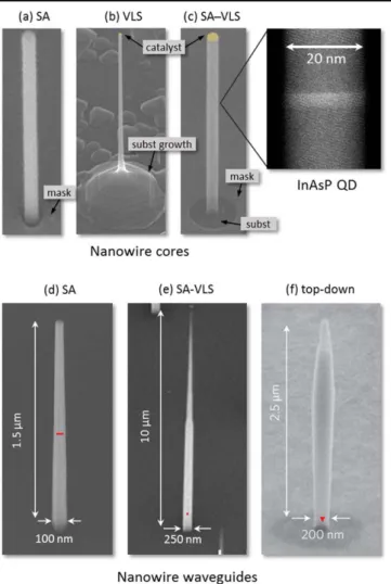
For bottom-up sources, the emitters are QDs defined by the grown nanowire (i.e. they form a segment of the nanowire core) allowing for complete control of the QD geometry (i.e. diameter, height) [88]. Importantly, sources based on
bottom-up nanowires inherently contain one emitter per device, and the emitter is precisely positioned on the waveguide axis. Waveguides are defined by switching from an axial (i.e. perpendicular to the growth substrate) to a radial growth mode such that the axially grown nanowire core acts as a template for the waveguide growth.
There are two basic bottom-up growth techniques: one based on selective-area (SA) epitaxy consisting of growth on a patterned substrate [89] and a second based on vapor–solid–
liquid(VLS) epitaxy [90] which uses metal particles to
cat-alyze the nanowire growth. The SA approach is by definition a site-controlled technique whereas the VLS approach was originally developed using randomly distributed particles [90–92] but is readily adapted to site-control using e-beam
patterning and metal lift-off[93].
In the SA approach the growth is typically performed on {111} zincblende (ZB) substrates or {0001} wurtzite (WZ) substrates with the polarity chosen to give vertical growth [89]. We note that the lattice-matching requirements for
defect-free growth in nanowire systems are greatly relaxed and growth of high quality material on dissimilar substrates, in particular III–V on silicon, has been demonstrated [94].
The substrate is coated with a mask, typically a dielectric like SiO2, which provides growth selectivity (i.e. no growth
occurs on the mask). This is patterned using e-beam litho-graphy to open up holes exposing the semiconductor surface. Under the appropriate conditions, growth on such a patterned substrate only occurs in the holes exposing the semiconductor surface, as shown infigure1(a). Growth conditions are
cho-sen to promote axial growth [95] and the QD inserted by
switching precursors from those required for the host semi-conductor to those for the dot material, e.g. from InP to InAs. The waveguide is then grown by cladding the nanowire with a shell using growth conditions that promote radial growth[95],
seefigure1(d).
In the VLS approach, vertically oriented nanowires are grown on cation-terminated{111} or {0001} substrates (e.g.
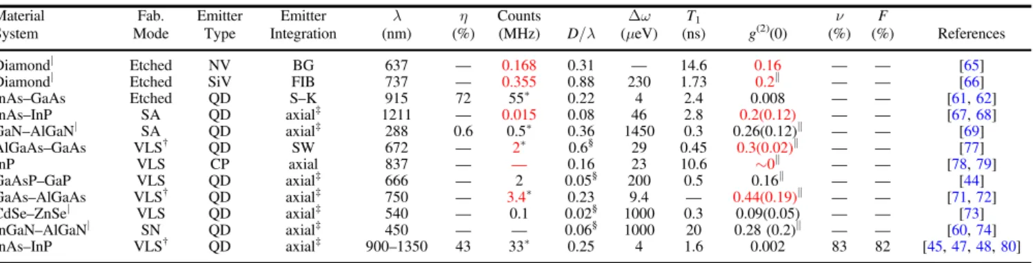
Table 1.Comparison of different top-down and bottom-up nanowire-based quantum light sources.
Material Fab. Emitter Emitter λ η Counts Δω T1 ν F
System Mode Type Integration (nm) (%) (MHz) D/λ (μeV) (ns) g(2)(0) (%) (%) References Diamond| Etched NV BG 637 — 0.168 0.31 — 14.6 0.16 — — [65]
Diamond| Etched SiV FIB 737 — 0.355 0.88 230 1.73 0.2P — — [66]
InAs–GaAs Etched QD S–K 915 72 55* 0.22 4 2.4 0.008 — — [61,62]
InAs–InP SA QD axial‡ 1211 — 0.015 0.08 46 2.8 0.2(0.12) — — [67,68]
GaN–AlGaN| SA QD axial‡ 288 0.6 0.5* 0.36 1450 0.3 0.26(0.12)P — — [69]
AlGaAs–GaAs VLS† QD SW 672 — 2* 0.6§ 29 0.45 0.3(0.02)P — — [77]
InP VLS CP axial 837 — — 0.16 23 10.6 ∼0P — — [78,79]
GaAsP–GaP VLS QD axial‡ 666 — 2 0.05§ 200 0.5 0.16P — — [44]
GaAs–AlGaAs VLS† QD axial‡ 750 — 3.4* 0.23 9.4 — 0.44(0.19)P — — [71,72]
CdSe–ZnSe| VLS QD axial‡ 540 — 0.1 0.02§ 1000 0.3 0.09(0.05) — — [73]
InGaN–AlGaN| SN QD axial‡ 450 — — 0.06§ 1000 20 0.28(0.2)P — — [60,74]
InAs–InP VLS† QD axial‡ 900–1350 43 33* 0.25 4 1.6 0.002 83 82 [45,47,48,80]
Material system— | indicates sources that have demonstrated room temperture operation.
Fabrication mode— SA: selective-area, VLS: vapor–liquid–solid, SN: spontaneous nucleation. † indicates VLS that also utilizes an oxide mask. Emitter type— NV: nitrogen vacancy, SiV: silicon vacancy, QD: quantum dot, CP: crystal phase dot.
Emitter integration— BG: background, FIB: focused ion beam, S–K: Stranski–Krastanow, SW: sidewall quantum dot. ‡ indicates emitter incorporation modes where the number of emitters is controlled.
λ — emission wavelength.
h — source efficiency.
Counts— color indicates continuous wave (CW)(red)or pulsed(black) excitation. Count rates at first lens are marked with a*, otherwise detection location was not specified.
D/ l — normalized waveguide diameter. § indicates nanowires transferred from the growth substrate and measured from the side.
w
D — emission linewidth. T1— radiative lifetime.
g(2)(0) — second order correlation. Values in parenthesis are corrected for background and detector timing response. Color indicates CW(red)or pulsed(black) excitation. indicates excitation power below saturation or not specified.
n — two-photon interference visibility.
(111)B / Group V-terminated) of the same material system. As above, defect-free growth on dissimilar substrates (e.g. III–V on silicon [92]) has also been demonstrated. Using
appropriate conditions, growth only occurs at the metal-semiconductor interface in a layer by layer fashion [96, 97]
allowing for nanowire growth with dimensions dictated by the size of the catalyst as shown infigure1(b). QDs are included
as above by switching precursors from the host to the dot material. In this way, QDs with abrupt interfaces and lateral dimensions corresponding to the nanowire core can be incorporated[34].
For completeness, we note two alternative avenues for integrating QDs in VLS-based nanowires. The first uses crystal phase(CP) QDs [78,79] where confinement is
pro-vided by band-offsets of the same material in different CPs (e.g. ZB versus WZ), discussed below. Here, control of the
number of emitters is not straight forward[98] and a route to
providing lateral confinement in the case of a QD in a waveguide structure is not evident as the dots are essentially planar defects which will propagate into the cladding. The second alternative integration method relies on QD formation on the sidewalls of the nanowire in a radially grown hetero-structure[77] via a strain-driven growth similar to that used to
grow dots in inverted pyramids[36]. This method, however,
does not provide the two major advantages normally asso-ciated with bottom-up nanowires, namely control of the number of QDs and their optimal position within the nano-wire for maximum coupling to the fundamental wave-guide mode.
As with SA nanowires, the VLS nanowires are clad using growth conditions that promote radial growth. In this growth mode there always exists a competition between substrate growth and VLS growth, evident infigure1(b). As the
con-ditions required to promote radial growth also tend to promote substrate growth, this makes it difficult to controllably clad the nanowires. A variation on the growth mode combines SA and VLS epitaxy[99]: holes are patterned in an oxide mask as
in the SA approach and catalysts are deposited in the center of these holes using a self-aligned lift-off process. This growth mode can be used to control where substrate growth can occur (e.g. the annulus of exposed substrate observed in figure1(c)),
allowing for the growth of waveguides tailored to the emis-sion wavelength of the QDs [47, 48]. Furthermore, by
con-trolling the relative axial, radial, and substrate growth rates, waveguides with well-defined tapers can be obtained, figure1(e). Both of these aspects play a crucial role in device
efficiency, as discussed section3.
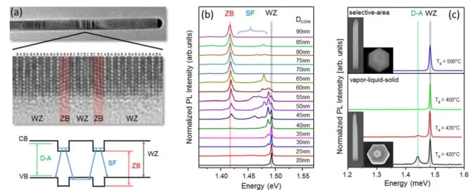
Binary semiconductor nanowires grown using VLS epi-taxy are known to exhibit a polytypic crystal structure[100]:
they contain segments of both ZB and WZ CPs. WZ and ZB in the 111á ñ direction differ only in the stacking sequence of the bilayers that make up the semiconductor and an insertion of one phase in the other constitutes a stacking fault(SF). The density of SFs will depend on nanowire diameter, growth conditions and material system[101,102]. For example, InP,
which is ZB in bulk, transitions to a WZ crystal structure for small nanowire diameters. This occurs through the appear-ance of WZ insertions in a predominantly ZB nanowire which, with decreasing diameter, transition to ZB insertions in a predominantly WZ nanowire shown infigure2(a). Since
the bandgaps of the two crystal phases are different, this transition can be observed in photoluminescence(PL) spectra of nanowires with different core diameter, as shown in figure2(b).
The presence of SFs has a profound effect on the optical properties of nanowire-based quantum emitters. For example, the band alignment for the WZ InP material system (lower panel of figure2(a)) is such that SFs (ZB insertions) act as
electron traps. For above-band excitation there will be a time-varying occupation of these traps with electrons that are free to move in the cross-section of the nanowire, resulting in a fluctuating charge environment for any QD in close proxi-mity. This will lead to significant spectral wandering of the QD emission wavelength, severely limiting two-photon
Figure 1.Upper panel: scanning electron microscopy(SEM) images of InP nanowire cores showing the different bottom-up growth modes:(a) SA—selective-area; (b) VLS—vapor–liquid–solid; and (c) SA–VLS which combines VLS growth with an oxide mask . The inset on the right shows a high resolution transmission electron microscopy(HRTEM) image of an InAsP QD embedded in an InP nanowire core. Lower panel: SEM images of nanowire waveguides based on(d) bottom-up nanowires grown using SA growth. Reproduced from[68]. © IOP Publishing Ltd. All rights reserved. (e) Bottom-up nanowires using SA–VLS growth and (f) top-down nanowires. Reprinted by permission from Springer Nature Customer Service Centre GmbH]: Springer Nature [61] (2010).
interference, discussed in section 5. The quantum emitters should therefore be incorporated in pure phase nanowires. For small diameter nanowires this is readily achieved using appropriate growth conditions[47] but becomes increasingly
difficult as the diameter increases. This means that to obtain a large enough diameter nanowire for good waveguiding, see section 3, requires a core–shell approach, where a small diameter pure WZ phase nanowire core is first grown fol-lowed by radial growth to form a shell. This lateral growth is commensurate with the crystal structure of the core resulting in a large diameter, pure WZ phase nanowire waveguide.
Finally VLS epitaxy is typically performed at lower temperatures compared to conventional growth resulting in a lower quality material. Impurities and crystal defects incor-porated in low temperature grown material [103] lead to
shallow donor and acceptor(D–A) levels which are evident in PL (see figure 2(c)). As with SFs, the trap population
dynamics limit two-photon interference by creating a varying charge environment. Growth at higher temperatures using conventional VLS epitaxy is difficult due to competition between growth at the metal-semiconductor interface and growth on the substrate. However, using SA–VLS, where substrate growth is limited, growth temperatures approaching those used in conventional high material quality epitaxy can be achieved[99].
3. Source efficiency
It is highly desirable for a quantum light source to produce a large photonflux coupled into the optical system of choice. The maximum flux will be limited by three parameters: (1) the internal quantum efficiency of the emitter, (2) the spontaneous emission rate of the emitter, and(3) the efficiency of coupling those emitted photons into the external optical system. We define the source efficiency, η, as the number of photons col-lected by the external optical system each time the emitter is
excited. The generated photons will couple to the available photonic modes of the nanowire waveguide (figure3(c)) with
efficiency βmode. For single mode operation [53] where the
waveguide is designed to confine only the fundamental mode HE11, the source efficiency can be written as
, 1
HE11 IQE
h=ab h ( )
where bHE11 is the fraction of photons emitted into the HE11
mode,α is the fraction of these photons that are coupled to the external optical system, and ηIQEis the internal quantum ef
fi-ciency of the emitter. For high quality QD materialηIQEis close
to 100%.
The maximum collection efficiency α will be limited to 50% using the standard nanowire geometry as half the emission is directed downwards toward the substrate. Although it entails added complexity in the fabrication, this 50% loss can largely be recovered using a back mirror deposited on the bottom of the nanowire[61,76,104]. Using
a strictly cylindrical waveguide design will further reduce the collection efficiency due to (1) back reflections from the top of the nanowire and(2) the large divergence of the mode (i.e. losses due to limitations in the numerical aperture of the collection optics). These can both be reduced by introducing a taper along the nanowire length(see figure3(a)) to expand the
mode, limiting its divergence as it exits the nanowire [53, 105]. Alternatively, the HE11 mode can be expanded
using an inverted taper approach [63] although this then
requires an antireflection coating to reduce backreflection. Together, these two design considerations provide a route to fabricating sources with near-unity collection ef fi-ciency[106].
HE11
b is given by the spontaneous emission rate into the fundamental mode,GHE11, relative to the emission rate into all
modes: , 2 HE HE HE 11 11 11 b g = G G + ( )
Figure 2.(a) Upper panel: HRTEM image of the crystal structure in a mixed-phase InP nanowire showing ZB insertions (i.e. stacking faults)
in a predominantly WZ crystal. Lower panel: Corresponding bandstructure showing the WZ–ZB band alignment and optical decay channels. (b) Spectra from InP nanowire waveguides showing the transition from pure WZ to pure ZB crystal structure as a function of the nanowire core diameter.(c) Spectra from InP nanowire waveguides grown at different temperatures. Material quality, as measured by the D–A emission peak, improves with increasing growth temperature.
whereγ corresponds to all other modes. Calculated values for ,
HE11 HE11
b G andγ as a function of the normalized waveguide diameter, D/λ, are shown in figure3(c) after [106] (see also
[48]). D is the waveguide diameter and λ is the wavelength of
the emitter. The emission rates are calculated atλ=950 nm for the InP material system and have been normalized with respect to values in bulk. From the figure, it is evident that high efficiency devices can be obtained for a large range of diameters with peak values ofbHE11=95%for D/λ∼0.25. The values ofbHE11 calculated here assumes that the QD is
centered laterally in the nanowire, i.e. at the peak of the optical mode. Any off-center positioning will result in a reduction of the coupling to the HE11 mode and potential
coupling to higher order modes (TE TM01, 01), resulting in
poorer efficiency.
As mentioned above, efficiency alone is not a complete measure of source performance; a high spontaneous emission rate of the emitter is also important for a high photonflux. As figure 3(c) shows, the spontaneous emission rate of the
emitter is dependent on the normalized diameter via the Purcell effect[107] (i.e. the overlap of the optical mode with
the emitter). In particular, the rate is inhibited for D/λ<0.24 which results in long radiative lifetimes[108,109] and a drop
in the measured count rates[48]. Therefore, whilst a source
may be very efficient over a large range of D/λ, the max-imum number of photons emitted from the source per unit time will depend strongly on D/λ.
A better measure of device performance is photon number per second collected by the optical system, Φp.Φp
will depend not only on source efficiency but also on the
spontaneous emission rate of the 2-level emitter and the probability pethat it is excited:
p p T , 3 p e HE e 1 11 h h F = G = ( ) where T1is the radiative lifetime of the transition. According
to equation(3), to maximizeF sources should be operated atp
excitation powers where pe is maximum (i.e. at saturation)
and, from of figure3(c), nanowire waveguides should have
normalized diameters D/λ∼0.24 whereGHE11=0.88Gbulkis
maximum.
The optimal geometry having D/λ=0.24 and including a tapered top(figure3(a)) is obtained in top-down approaches
using well-understood lithography and dry-etching processes [61]. It is less trivial to obtain this geometry using bottom-up
growth approaches. As mentioned in section2.2, a two-step nanowire growth process is essential, where an initial step in an axial growth mode is used to grow a nanowire core and define the QD and a second step in radial growth mode is used to grow a cladding to define the nanowire waveguide. Independent control of axial and radial growth rates and their ratio are necessary to define the core (i.e. the QD), the clad-ding(i.e. waveguide) and to taper the waveguide, as discussed in section 2.
The source efficiency η can be determined from the integrated PL intensity using pulsed excitation to extract the average number of photons emitted per excitation pulse. To ensure the emitter is excited with each pulse, excitation powers that saturate the 2-level transition are used. For sources based on defects, one typically uses the integrated counts in the zero phonon line (ZPL) (e.g. λ=637 nm at
Figure 3.(a) Schematic of a tapered nanowire waveguide showing emission channels into confined (GHE11) and leaky (γ) modes.
(b) Refractive indices of the confined modes as a function of normalized waveguide diameter, D/λ. Inset shows the electric field intensities of the modes.(c) Normalized spontaneous emission rates calculated for an InP waveguide at an operating wavelength of λ=950 nm. (d) PL spectrum and(e) detected count rates in the zero-phonon neutral and charged exciton lines for CW (solid square) and pulsed (open square) excitation.
300 K for NV centers). For QDs without charge state control [110], the ground state emission in a time-integrated
photo-luminescence measurement can show different excitonic charge complexes depending on the background doping and Fermi level pinning. For an accurate determination ofbHE11,
all contributing excitonic complexes should be included. Excitation with a continuous wave(CW) source is more appropriate for determining the maximum attainable Φp in
that it represents the maximum pulse rate at which the source can be excited[111] (i.e. with CW excitation, the emission
rate is limited by the emitter lifetime as opposed to the excitation pulse repetition rate).
An example of determining device performance is shown infigures3(d) and (e) for a high efficiency source consisting
of a tapered InP waveguide with D/λ=0.24 with an embedded InAsP QD. Figure3(d) shows the time-integrated
PL spectrum from the dot which emits from two charge complexes: the neutral (X) and negatively charged (X-) exciton, distinguished by their exchange splitting [83].
Figure3(e) shows the detected integrated intensity of the ZPL
for X and X-as a function of excitation power for both CW and pulsed excitation. Table2lists the ZPL counts at thefirst lens (i.e. with the spectrometer and collection optics throughput of 10% accounted for) at saturation for both charge complexes and both excitation methods.
Using the counts in the ZPL(i.e. from a lorentzian fit of the spectrally resolved PL peak) neglects emission into pho-non sidebands which can account for 20% of the total counts at a temperature of 4 K [3]. Alternatively, integrated counts
can be determined using single-photon avalanche diodes where the fraction of phonon-assisted emission counted will depend on the width of the spectral filter used. For some applications phonon-assisted emission does not impact sys-tem performance, but where indistinguishable photons are required(section5), performance will be degraded.
An efficiency of η=31% is obtained from the ratio of the ZPL intensity of X and X- combined to the pulse repe-tition rate of 80 MHz. This measurement is only accurate for a source where multi-photon emission is not observed up to saturation, see section 4. From equation (1), the measured
collection efficiency is α=32.6%, assuming bHE11=0.95 and ηIQE=1. The maximum collection efficiency for this
device design (i.e. no back mirror) and including only the counts in the ZPL (i.e. neglecting emission in the phonon sidebands) is αmax=0.4, corresponding to a maximum
efficiency for the device of ηmax=38%, just 7% higher than
measured.
The count rates in the ZPL using CW excitation(i.e. Φp)
increase by 3.3x for X and 1.8x for X-. This increase
compared to pulsed excitation is consistent with the measured lifetimes of T1∼2.5 ns giving a decay-limited excitation rate
of 400 MHz and an ultimate bound on increased intensity of 5x.
We note that this exercise is to evaluate the source design: in real devices, η andF need to be specip fied for a
given transition and will be lower for devices emitting from different charge complexes. This efficiency loss can be recovered using devices with charge state control[112].
Efficiencies exceeding 70% have been obtained from nanowire sources based on the top-down approach using the X transition [61] whilst bottom-up approaches have
demon-strated efficiencies exceeding 40% using the X- transition [45, 76]. The state-of-the-art top-down nanowire sources
employed a back mirror whilst the devices in[45] did not. As
such, the efficiencies demonstrated with both top-down and bottom-up approaches represents close to the ultimate per-formance possible. This level of perper-formance is on par with state-of-the-art sources based on QD micropillar cavities which have achieved efficiencies of close to 80% [113].
However, there is a trade-off between the conditions which give maximum efficiency (e.g. typically above-band excita-tion at powers that saturate the 2-level transiexcita-tion) and those that optimize the quantum properties. Efficiencies and quantum properties(section4through section6) both need to
be specified in order to make meaningful comparisons between platforms Ideally, a metrology-based approach should be established in order to standardize the character-ization methodology of non-classical light sources and allow for a true comparison of the various platforms.
Unlike nanowire devices, sources based on micropillar cavities benefit from Purcell-enhanced emission rates. Typical lifetimes for QDs in high efficiency micropillar sources are a few hundred picoseconds[113] with shorter lifetimes possible
using photonic crystal cavities[114]. These values are much
lower than those reported for high efficiency nanowire devi-ces (see table 1). Thus, cavity-based sources will greatly
outperform nanowire devices in terms of emission rates (i.e.
p
F). Efforts to combine nanowires with cavities to provide Purcell enhancements and wavelength discrimination are discussed in section7.
4. Single photon emission
High single photon purity (i.e. low probability of emitting multiple photons) is a prerequisite for any quantum light source. Ideally, the source should emit exactly one photon at a time into a given spatiotemporal mode on demand. For some quantum cryptographic communication protocols (e.g. BB84 [115]), high single photon purity is sufficient. Two photon
correlation events are quantified by the second-order corre-lation function, g( )2( )t , which, for a single mode opticalfield
characterized by creation and annihilation operators aˆ†and aˆ,
is defined by g a t a t a t a t a a , 4 2 2 t = á +t +t ñ á ñ ( ) ˆ ( ) ˆ ( ) ˆ ( ) ˆ ( ) ˆ ˆ ( ) ( ) † † †
Table 2.Counts atfirst lens in the ZPL at saturation. Exciton Counts(CW) Counts(pulsed) Efficiency, η
(Mcps) (Mcps) (%)
X 15.1 4.6 5.7
X- 36.6 20.2 25.3
where á ñ· denotes the statistical average. In the case of photon number states, n∣ ñ,g( )2( )t provides a measure of the
multi-photon emission probability. In particular, the correlation function dips at zero delay, g( )2(t =0),(i.e. the photon sta-tistics display antibunching):
g n
n n
0 1 1 1. 5
2 ( )= - = - ( )
( )
Hence, for any given Fock state with n>1,g( )2( )0 1 2. This is used to argue that g( )2( )0 1 2implies single photon emission. However, practical sources require, as a minimum, g(2)(0) values of less than 0.1 [4].
Photon emission statistics are measured using a Hanbury Brown-Twiss(HBT) interferometer [116] where the photons
are directed to the input of a beamsplitter with the outputs directed to two single photon detectors. Timing electronics are used to count and correlate detection events between the two detectors. Figure 4(a) shows the time-correlated counts
from a nanowire source using CW(upper panel) and pulsed (lower panel) excitation [117]. For CW excitation, the
multi-photon emission probability is determined from g( )2(t =0) whilst the time-dependence gives the decay rate of the transition. A g(2)(0) derived from a CW measurement post-selects only those photons that arrive simultaneously atτ=0 convoluted with the temporal response of the detectors. To achieve on-demand operation, pulsed excitation has been proposed [118] to generate a regulated stream of single
photons. The multi-photon emission probability in a pulsed g(2)(τ) measurement is determined from the ratio of the area of the peak at τ=0 to that of the adjacent peaks. We will refer to this probability as g(2)(Δτp). Pulsed g(2)(τ)
measure-ments provide additional information on the photon statistics, e.g. re-excitation of the emitter within the same pulse cycle [119–121] which appears as a characteristic double-peaked
feature around the dip atτ=0 [119].
A prerequisite for a perfect single photon source(i.e. zero multi-photon emission) is the isolation of a single 2-level emitter. This includes both spatial isolation of a single emitter as well as spectral isolation of a single transition from that emitter. In this context, bottom-up nanowires using QD
emitters are close to ideal. A single emitter is incorporated by design and in high material quality QDs at low temperatures (e.g. 4.2 K), the different excited complexes (such as X X, -or XX) do not spectrally overlap and are readily spectrally filtered. A multi-photon emission probability of g( )2(Dtp) =0.002 with an efficiency of 43% has been demonstrated using the SA–VLS approach [45, 47] with InAsP QDs emitting at
λ=950 nm. This widely tunable system has also been used to demonstrate single photon emission in the telecom O-band, with a measured g(2)(Δτp)=0.02 at λ=1340 nm [48].
Isolating a single emitter when using the top-down fab-rication approach with randomly nucleated self-assembled QDs is more of a challenge than for the bottom-up approach. A QD density needs to be targeted that minimizes the number of emitters per device (to limit the possibility of several emitters contributing to a non-zero g(2) [63]) but also
mini-mizes the number of empty devices. This will affect device yield. Furthermore, as the position of the QD within the waveguide is random, efficiencies from device to device will vary depending on how well the emitter is coupled to the optical mode [87]. Even with these concerns, devices based
on the top-down approach using self-assembled QDs have demonstrated state-of-the-art multi-photon emission of g(2)(Δτp)=0.008 at an efficiency of 72% [61]. The device
yield aspect distinguishes top-down and bottom-up approa-ches, as highlighted infigure4. In the bottom-up approach the yield of working devices is nearly 100%: each nanowire contains a single emitter and each emitter is optimally posi-tioned in the waveguide for maximum coupling to the HE11
mode. Consequently, all sources show similar count rates at saturation and g(2)(Δτp) values of less than a few percent.
High efficiencies have also been demonstrated using micropillar cavities when excited above-band, as mentioned in section 3. Unlike nanowires, however, these devices [113,122] exhibit increased g( )2(Dtp)values when excited at
powers whereΦpis maximum(i.e. at saturation). With
above-band excitation, the system is flooded with carriers which, if they persist for times comparable to the exciton lifetime, can be captured by the QD after the first excitonic photon has been emitted[119,120]. This will increase g(2)(Δτp). Cavity Figure 4.(a) Second-order correlation measurements from a nanowire QD for CW (upper panel) and pulsed (lower panel) excitation.
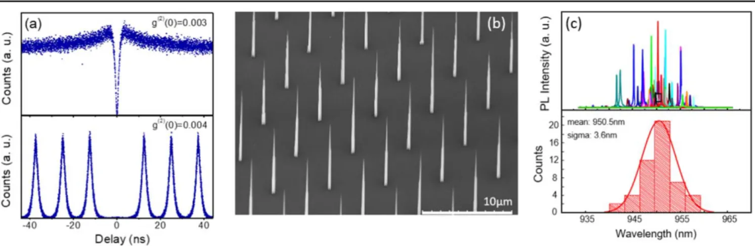
Reproduced with permission from[117]. (b) SEM image of an array of nanowires showing unity growth yield. (c) Upper panel: spectra from 50 nanowire QDs showing unity emission yield. Lower panel: histogram of the corresponding emission wavelengths.
structures can promote such re-excitation by decreasing the QD exciton lifetime,(as is demonstrated in a comparison of on and off resonance g(2)(τ) measurements in [118] and
[122]). Additionally, cavity effects may increase the lifetime
of off-resonant excitons in nearby traps(e.g. in the wetting layer [122, 123]) which can also lead to re-population of
the QD.
In order to achieve the high single photon purity at maximum F observed in nanowire systems, microcavityp
devices have employed electric fields and/or resonant exci-tation[27,28]. Recent results with electric field tuned QDs in
cavities[27] show improved performance at saturation with
g(2)(Δτp)=0.024 measured in devices operating at 65%.
This suggests that the electric field used for tuning is sweeping away excess carriers from the region around the QD that were generated by the above-band excitation.
Using resonant excitation [120], on the other hand,
avoids re-population of the excited state within the same pulse cycle by directly loading the excited state. Resonant fluores-cence, however, requires rejection of the pump laser and for rejection based on polarization[124] results in a 50% drop in
efficiency. Hence, state-of-the-art micropillar cavities with single photon purities comparable to nanowires operate at reduced efficiencies of 15%–37% [27,28]. Recovery of this
loss should be possible with a rejection of the pump that is based on orthogonal excitation and emission directions [18, 125]. Alternatively, asymmetric microcavities systems
can be employed to preferentially generate photons in a single polarization state[126].
The absence of cavity effects and wetting layers in bot-tom-up nanowires may contribute, together with being a uniquely single emitter device, the high single photon purity observed in nanowire systems using above-band excitation at maximumF .p
5. Indistinguishable photon emission
In many applications, the emitted photons from quantum sources are required to be identical in all degrees of freedom [11] (i.e. perfect overlap of the photon wave-packets in
energy, time, space, polarization). Secure communication schemes such as quantum repeater-based entanglement dis-tribution [127] and measurement-device-independent
quant-um key distribution [128] rely on such indistinguishable
photons as do quantum computing schemes based on linear optics [129]. Factors limiting the ability to generate
indis-tinguishable photons in nanowires, and solid state systems in general, include charge noise and interactions with acoustic phonons [130, 131]. If these decoherence mechanisms are
present, the emitted photons will not be lifetime-limited and emission energies will be time-dependent (i.e. the optical linewidths will be broadened).
Charge noise can be caused by a time-dependent popu-lation of traps near the emitter which produces afluctuating charge environment and leads to spectral wandering of the emission energy. In top-down nanowire sources based on
self-assembled QDs, these traps are due to impurity-related defects, the wetting layer, or other dots. In bottom-up nano-wires, charges can also be trapped in SFs, as discussed in section 2. The dramatic effect of SFs on the emission line-width of a QD in a VLS-grown nanowire is shown in the upper panel offigure5(a). For mixed-phase nanowires [132]
having SF densities of a few tens per micron, measured linewidths are Δω>400 μeV and vary immensely from nanowire to nanowire depending on the proximity of a SF to the QD. In pure phase nanowires[45,47] (SF densities of less
than 1μm−1), the linewidth collapses by over two order of magnitude to Δω∼4 μeV, close to that expected for a radiative lifetime of T1∼2 ns.
The coupling of acoustic phonons to the optical transition associated with a 2-level system results in emission into sidebands around the ZPL. While phonon absorption can be eliminated at sufficiently low temperatures, the emission process will persist. At 4 K, emission into the phonon side-bands can be 20% of the total emission [3], see figure5(b).
Coupling to phonons shifts the energy of the emitted photon with a corresponding decrease in indistinguishability.
The level of indistinguishability between two photons is determined from a two-photon interference measurement [133] and for a pulsed measurement is quantified [134] by the
visibility,ν: g g g , 6 2 2 2 n t t t = D - D D ^ ^ ( ) ( ) ( ) ( ) ( ) ( ) ( ) where g2 Dt ( ) ( ) (g2 Dt ^ ( )
( ) ) is the integrated probability,
within a time windowΔτ about τ=0, of detecting photons at both outputs of a beamsplitter for indistinguishable (dis-tinguishable) photons at the two inputs. Perfectly indis-tinguishable photons will coalesce and exit the same output port, g(2)(Δτ)P=0, whereas distinguishable photons will have equal probabilities of exiting each output port,
g2 Dt =0.5
^
( )
( ) . An ideal source will have ν=1 over Δτ
covering the entire repetition period aroundτ=0 whilst any timing jitter in the relaxation process or dephasing in the 2-level transition will result in coincidence counts for
0
t
D ¹ . Here, dephasing is any mechanism that reduces the coherence time, T2, of the photon such that it is not
lifetime-limited(i.e. T2<2T1).
To date, two-photon interference measurements on nano-wires have been reported only for the bottom-up SA–VLS system [45]. Using above-band excitation from a 20 MHz
pulsed source, sequential photons delayed by 50 ns show low non-post-selected visibilities of ν∼4% when all the emitted photons are collected. The low value is a consequence of relaxation time jitter associated with above-band excitation and the presence of decoherence mechanisms discussed above. This results in a multi-peaked visibility measurement(see inset, figure5(c)) characteristic of two-photon interference from
non-lifetime-limited photons [26]. Improved visibilities can be
achieved using temporal post-selection where only the photons received within a small time delay around τ=0 are used. Since many of the photons are being thrown away this results in a drop of the source efficiency (figure5(c)). A visibility of
ν∼80% was obtained at a device efficiency of 10%, similar to other state-of-art broadband approaches using above-band excitation[135].
This level of performance is significantly lower than state-of-the-art QD micropillar cavities which have achieved extremely high levels of indistinguishability (ν>98%) in devices operating at efficiencies of 15%–33% [27,31].
Near-unity non-post-selected visibilities in these devices have only been achieved through resonant pumping schemes in com-bination with Purcell-enhanced spontaneous emission rates,
both of which help to mitigate the decoherence mechanisms cited above. As well as reducing relaxation timing jitter, resonant pumping avoids the charge fluctuations associated with above-band excitation, where the system isflooded with carriers with each excitation pulse. For example, visibilities in micropillar devices drop to ν=53% when exciting non-resonantly into the QD wetting layer[113] (where increased
timing jitter in the emission process for cavity environments [26] may also contribute to the decrease in visibility).
Purcell-mediated lifetime reduction may also mitigate the effects of a fluctuating charge environment by decreasing recombination times to levels potentially lower than the time scales asso-ciated with charging events. This same increase of the spontaneous emission rate into the cavity mode will also limit phonon emission and absorption processes[24].
To obtain higher visibilities in nanowire devices, higher quality material is required to reduce defect-related trap density and attain lifetime-limited emission linewidths. Improving material quality can be achieved using higher temperature growth as discussed in section 2. Alternatively, post-growth annealing-mediated intermixing has been sug-gested as a route to remove grown-in defects from nanowires [136]. Additionally, techniques to stabilize the charge
environment can be employed, for example, 2-color excita-tion [113] where visibilities as high as ν=80% have been
achieved in devices operating at efficiencies of 79%. Near-unity visibilities, however, will require resonant excitation to eliminate relaxation timing jitter. Resonant excitation in other broadband QD-based devices [19, 137] has demonstrated
non-post-selected visibilities exceeding 90%. Ideally, the excitation scheme would employ rejection techniques that do not sacrifice device efficiency [18, 125, 126]. Resonant
excitation of nanowires[62,138,139] has yet to be applied to
two-photon interference measurements.
High efficiency devices operating at high repetition rates will ultimately require nanowire-cavity coupled systems. Cavity structures can mitigate phonon-assisted emission[24]
which is normally discarded in broadband devices through spectrally filtering. Using emitter-cavity systems will make resonant excitation mandatory in order to reduce timing jitter in the emission process due to long-lived(off-resonant) states populated at excitation powers where F is maximump [26].
Nanowire-cavity systems for generating quantum light have yet to be demonstrated (see section 7 for possible routes to on-chip nanowire integration).
Finally, two-photon interference measurements are typi-cally quoted for sequential photons emitted from the same source, over short(a few ns) time intervals between photons. However, it is the indistinguishability on longer time scales [29,30,130], as well as indistinguishable photons generated
by remote sources[140,141], that are required in the
appli-cations listed above. For remote sources, tuning methods will be required as the emission energies from nominally identical nanowire devices vary by several meV as shown in figure4(c). Tuning the emission energy of nanowire sources
has been demonstrated using techniques adopted from self-assembled QDs devices and include both permanent[79,136]
and dynamic[64,142] approaches. Figure 5.(a) PL spectra from a QD in a mixed crystal phase
nanowire(from [132]) and in a pure WZ nanowire (from [47]). Insets show corresponding HRTEM images of the crystal structure. (b) PL spectrum from the dot on a logarithmic scale showing phonon emission and absorption sidebands. Blue curve is afit to the ZPL. (c) Dependence of the two-photon interference visibility on source efficiency (i.e. amount of temporal post-selection). Inset shows the coincidence counts(i.e. 1-n) in the zero-delay peak obtained using above-band 20MHz pulsed excitation, from[45].
6. Entangled photon pair emission
Entangled photons are required for certain quantum crypto-graphy protocols [143, 144], quantum repeaters [127] and
certain quantum computing schemes[145,146]. Each of the
degrees of freedom of a photon can be entangled(see [6]) and
for two-level systems, one typically employs polarization [147] or time-bin [148] entanglement.
Polarization-entangle-ment can be generated using post-manipulation of indis-tinguishable photons [149] or within the source itself (e.g.
using the XX− X cascaded emission in QDs [13,147]). In the
XX−X cascade, the polarization of the photon from the biexciton decay is entangled with that from the exciton decay to form a maximally entangled Bell state i.e.
Hxx Hx ei s Vxx Vx
1 2
yñ = ñ ñ + t ñ ñ
∣ (∣ ∣ ∣ ∣ ), where s is the ani-sotropic exchange splitting (AES) between the two inter-mediate exciton states(figure 6(a)) and τ is the time interval
between the biexciton and exciton emission.
The time-dependent phase factor due to a non-zero AES will limit the fidelity to a maximally entangled Bell state. AESs arise from any asymmetries in the system, for example, in the QD shape, composition, strain, or crystal structure. The bottom-up nanowire platform provides a route to the growth of highly symmetric QDs. The dot shape is dictated by the nanowire and not influenced by crystal lattice direction-dependent adatom mobilities, resulting in a highly circular in-plane geometry as shown in the inset of figure 6(b).
Fur-thermore, VLS nanowire QDs are typically grown in the WZ CP on {0001} WZ ({111} ZB equivalent) planes without wetting layers, providing higher axial symmetry compared to ZB S–K dots grown on (001) substrates. This high symmetry
is expected to manifest in a reduced AES[152]. Splittings of
SA–VLS grown InAs QDs in InP nanowires range from 1 to 10μeV with over 50% having splittings of <2 μeV [150], see
figure6(b). The likely origin of non-zero splittings is an axial
inversion anisotropy [153] due to phosphorus and arsenic
tailing inherent to the growth process.
The measure of entanglement is given by thefidelity to a maximally entangled state, determined from the cross-corre-lations between each of the transitions shown infigure6(a) as
a function of polarization basis using a polarization-resolved HBT-type measurement. The fidelity, F, is calculated from
F 1 Crectilinear Cdiagonal Ccircular 1
4
= ( + + - ) where C is the degree of correlation for a given polarization basis denoted by the subscripts. C is given by[154]:
C g g g g , 7 xx x xx x xx x xx x , 2 , 2 , 2 , 2 = -+ ( ) ( ) ( ) ( ) ( )
where gxx x( )2, and gxx x( )2, are the second-order correlation functions when detecting the XX photon(e.g. HXX) with a copolarized
(e.g. HX) and cross-polarized (e.g. VX) X photon, respectively.
Several nanowire systems have demonstrated correlated XX−X emission including devices based on SA growth [67,68] as well as CP QDs in VLS nanowires [79]. However,
to date, only the InAsP–InP system grown using the bottom-up SA–VLS technique has demonstrated entangled photon pair generation [80, 150,155] with reported fidelities to the
maximally entangled state of F>80% [80]. Higher fidelities
should be achievable using the various AES tuning techni-ques developed for QDs(see [156]) in order to eliminate the
small remaining splitting. Alternatively, which-path infor-mation can be eliminated even in QDs with a non-zero AES
Figure 6.(a) Polarization-resolved PL spectra from a nanowire QD with an anisotropic exchange splitting (AES)=8 μeV, from [47]. The inset shows the level diagram of the XX−X cascade. (b) Histogram of AESs from measurements on 16 nanowire QDs, from [150]. Inset is a top-view SEM of a nanowire core with the gold catalyst highlighted, showing high in-plane symmetry.(c) Comparison of the entanglement fidelity and photon-pair source efficiency of different entangled photon-pairs sources. The blue squares correspond to parametric down-conversion sources whilst the rest are QD sources. The two sources highlighted by the yellow ellipses are based on nanowire QDs. Reproduced from[80].CC BY 4.0.(Updated to include the recent results from [151] ( )).
by tuning the biexciton binding energy to zero[157,158], or
compensating for the phase term arising from non-zero AES through the use of rotating waveplates[159].
The photon-pair source efficiency from nanowire devi-ces, defined as the average number of photon pairs per excitation pulse collected into thefirst lens, is low at ∼0.3%. Although this compares well with other QD-based sources (see figure 6(c), after [80]), there is much room for
improvement. For a broadband device such as a nanowire this efficiency depends on the square of the single photon effi-ciency,η, since it is a two photon process, and on the ability to reliably excite the XX state with every laser pulse. This is further complicated for devices using cavities where both the XX and X have to emit within a cavity mode for good col-lection efficiency. With a typical nanowire η of 31% the maximum efficiency is 9.6% compared to a measured 0.3%, implying that the above bandgap excitation used results in low biexciton population fidelity. Key to achieving higher efficiencies are excitation schemes whereby the biexciton state is populated with unityfidelity [160].
Ultimately, 2-level systems should outperform para-metric down-conversion sources where efficiencies are limited due to the probabilistic emission process(i.e. higher efficiency comes at the expense of reduced fidelity due to multi-pair emission, see figure 6(c)). This was recently
demonstrated in a QD system using two-photon excitation (TPE) to coherently populate the XX state with high effi-ciency[151]. TPE together with the broadband operation of
nanowire devices (required to collect the energetically dis-tinct X and XX photons) should enable high efficiency nanowire-based sources of entangled photon pairs in the near future.
7. On-chip integration
As highlighted in the previous sections, nanowire sources would benefit from integration with optical microcavities. Coupling to microcavities would allow for operation at higher repetition rates as well as improve the indistinguishability of the emitted photons. Nanowires are typically grown perpendicular to the substrate (i.e. in a 111á ñ direction on a {111} substrate) and have large aspect ratios making mono-lithic integration difficult. This is in contrast to S–K QDs or defect-based emitters which are readily integrated on-chip using, for example, photonic crystal structures [16,161].
Growth of SA nanowires directly on Si waveguides has been proposed as an avenue for monolithic integration using as-grown nanowires perpendicular to the substrate[162]. Although
highly scalable, the coupling efficiency to the Si waveguide is low at 1%. Higher efficiencies will require growth of nanowires at non-normal directions to the substrate. This entails mod-ification of the growth substrate to expose the appropriate facets, for example, through etching [163] or template growth.
Non-normal growth has been demonstrated using ridge-type struc-tures[164] and even nanowires [165] as the template.
In the near term, a less scalable solution involves the transfer of nanowires from the growth substrate to a new sub-strate with pre-patterned alignment marks. Subsequent proces-sing is used to define appropriate photonic structures around the nanowires using the alignment marks as a reference, as shown schematically in figure 7(a), after [166]. Using this approach,
VLS-grown nanowires were embedded in SiN waveguides with a measured coupling efficiency from the nanowire to the waveguide of 24%, and a measured multi-photon emission probability of g( )2( )0 =0.07[166]. Once nanowire emission is coupled to a waveguide then photonic integrated circuits are
Figure 7.(a) Upper panel: schematic of an InP nanowire embedded in a SiN waveguide. Middle panel: FDTD simulation of the electric field
profile (Ex) in a SiN waveguide with an embedded QD. Simulated coupling efficiency for unpolarized emission from the QD to the SiN waveguide mode is 36%(18% for forward and backward directions). Lower panel: schematic of the pick and place transfer process. Reprinted with permission from[166]. Copyright (2016) American Chemical Society. (b) Upper panel: schematic of an InP nanowire on a SiN waveguide for evanescent coupling. Lower panel: FDTD simulations of the electricfield profile (Ex) for a device with 90% coupling to the waveguide mode(left) and SEM image of an evanescently coupled nanowire waveguide device (right).
readily envisioned. For example, dynamic routing of single photons has been demonstrated using a tunable ring resonator, as well as multiplexed single photon emission through the coupling of two nanowire sources into the same SiN waveguide[167].
An alternative approach, shown infigure7(b), relies on
evanescent coupling of the nanowire emission to a waveguide in a manner similar to that reported in[168]. There, epitaxial
layers containing S–K QDs were patterned with a taper to facilitate the transfer of the optical mode to an underlying SiN waveguide. In the nanowire case, the required taper can be obtained through growth, and for taper lengths of 10μm, coupling efficiencies of greater than 90% are predicted [169].
Importantly, combining this approach with a nanomanipulator having a sufficiently high positioning precision [170] would
greatly simplify the nanowire waveguide alignment process. This corresponds to an incremental increase in scalability in that it allows for the pre-fabrication of complex photonic circuits onto which pre-selected nanowires can be placed deterministically, rather than building the photonic circuit around the already positioned nanowires. Furthermore, eva-nescent coupling is compatible with ring resonator structures where Purcell-mediated emission rate enhancements of ∼6 are predicted from coupling to the whispering gallery modes of the resonator[168]. Alternatively, designs have also been
proposed whereby nanowire sources can be coupled to pho-tonic crystal waveguide and cavity structures[171,172] with
demonstrated eight-fold emission rate enhancements[172].
8. Multiple emitter nanowires
As mentioned in section 1, a unique feature of bottom-up nanowire growth is the ability to incorporate multiple, aligned
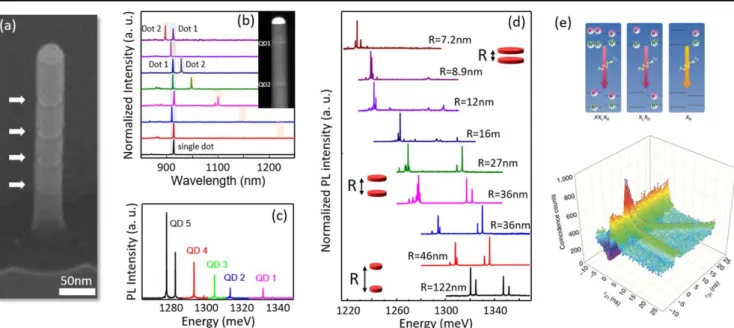
QDs optimally coupled to the same optical mode. Such structures, an example of which is shown infigure8(a), have
been demonstrated using the different bottom-up growth modes and in different material systems [44, 70,173, 174].
The separation between the QDs as well as their thicknesses and compositions can be reproducibly controlled through the epitaxial growth process, in contrast to results obtained when stacking S–K QDs [49].
The ability to control the composition of the individual QDs has been used to quantify the D/λ dependence of the spontaneous emission rate [48]. Using double QD structures
embedded in nanowire waveguides with diameter D, the emission energy of one of the dots was progressively shifted to longer wavelengths by increasing the arsenic content. The two dots were sufficiently separated to avoid electronic coupling. The observed decrease in intensity as the dot is red-shifted, shown infigure8(b), is consistent with the expected decrease
in the spontaneous emission rate shown infigure3(c).
Uncoupled, multidot structures also provide a route to developing sources with higher emission rates that do not rely on cavity-enhanced recombination rates. By incorporating multiple QDs in the same nanowire, each tuned to a different wavelength, sources based on wavelength division multi-plexing are possible. The number of channels will be limited by the number of uncoupled QDs that can be incorporated in a single nanowire and the channel spacing will be limited by the linewidths of the emitters. A PL spectrum of a 5-channel device is shown infigure8(c). In order to achieve
linewidth-limited channel densities, charge state control will be required to avoid emission from different charge complexes(e.g. X and
X-, see QD5 infigure8(c)).
Precise control of the interdot spatial separation and the QD emission energy can also be used to study coherent
Figure 8.(a) SEM image of an InP nanowire containing four InAsP QDs selectively etched to highlight the dots. (b) Emission spectra of
double QD nanowires used to quantify the D/λ dependence of waveguide-mediated spontaneous emission rates. Reprinted with permission from[48]. Copyright (2018) American Chemical Society. (c) PL spectrum of five QDs in one nanowire emitting into the same waveguide mode.(d) PL spectra from nanowire-based QD molecules as a function of the separation between the dots (R), from [175]. (e) Three-photon coincidence measurements from a QD molecule. Reproduced from[176].CC BY 4.0.
coupling in QD molecules. Compared to molecular systems based on coupled S–K QDs [49, 177,178], nanowire-based
coupled dot systems offer better control of the alignment and separation between the two emitters [179] as well as the
potential for stronger interactions mediated by the waveguide [175]. Evidence of coherent coupling has been reported in the
InAsP/InP nanowire system [175] where clear spectral
splitting of the uncoupled QD resonances are observed with decreasing interdot spatial separation, seefigure8(d).
A potential application of molecular QD systems is for generating multipartite photon states without involving the excited levels of a QD. Triexcitons can be formed from the ground states of two coupled QDs, leading to the sequential emission of three strongly correlated photons. Generation of photon triplets has been demonstrated using coupled InAsP QDs in an InP nanowire [176]. The time-correlated triplet
emission shown infigure 8(e) is the first step towards high
efficiency sources of three-photon entangled states. 9. Conclusions and outlook
Thefield of nanowire-based quantum light sources has seen significant progress since the first demonstration of single photon emission from a nanowire QD in 2005 [44]. The
superior scalability, in particular the near-unity yields, of bottom-up nanowire devices has been established. Impor-tantly, pathways to eliminating existing limitations are clearly identified. Fourier-limited transitions should be possible with improved material quality available at higher growth tem-peratures. Two-photon interference measurements using strictly resonant excitation have yet to be performed on a nanowire device. Together, these improvements should lead to near-ideal indistinguishability independent of the temporal separation between photons and provide a pathway to gen-erating indistinguishable photons from remote sources. They are also expected to improve the efficiency and fidelity of entangled photon pair sources.
The route to monolithic integration has yet to be clearly identified. Although the ability to pick up and position a single quantum emitter is undeniably impressive and immensely useful for development, it should not be con-sidered a genuinely scalable solution. A scalable on-chip platform lies in growth architectures compatible with designs of photonic structures that can provide high coupling ef fi-ciencies. The growth of nanowires oriented parallel to the growth substrate will greatly facilitate progress in this area, allowing for new design concepts for coupling to waveguide and cavity structures. This geometry is also more suited to the incorporation of electrical contacts and gates, important for charge state control in nanowire QDs[112].
Ideally QD nanowires should be integrated with the silicon-on-insulator (SOI) platform and use silicon as the waveguiding material. This will entail developing sources operating at telecom wavelengths (e.g. λ=1550 nm). Quantum sources in this wavelength range have been demonstrated with S–K QDs using the InAs/InP material system[180] and, in principle, should also be attainable using
the nanowire platform. To date, single photon emission from the nanowire system has been demonstrated for wavelengths up to λ∼1350 nm [48], already compatible with SOI
pho-tonic circuits.
An SOI-based nanowire platform would be ideal not only for on-chip optical quantum computing [181, 182] and
quantum simulation[183,184] but will also be beneficial for
quantum communication where one can envision sources integrated with on-chip measurement to test the relevant quantum properties [185] combined with efficient off-chip
coupling into low-loss telecom fibers [186,187] using fixed
alignment-free techniques forfield-deployable, real devices. Finally, multiple emitters mutually coupled to the same optical mode of a nanowire waveguide is an area only recently being explored. The growth-related spectral splittings of uncoupled emitters need to be disentangled from interac-tion-mediated splittings[175]. This can be done, for example,
with an additional tuning mechanism for controlling the resonance energy of the emitters [178]. Coupling QDs
toge-ther opens up a richfield of coherent coupling effects relevant for future photonic quantum technologies that require multi-ple interacting emitters.
ORCID iDs
Dan Dalacu https://orcid.org/0000-0001-6204-3952
References
[1] O’Brien J L, Furusawa A and Vučković J 2009 Nat. Photon. 3 687
[2] Beveratos A, Abram I, Gérard J-M and Robert-Philip I 2014 Eur. Phys. J. D68 377
[3] Lodahl P, Mahmoodian S and Stobbe S 2015 Rev. Mod. Phys. 87 347
[4] Aharonovich I, Englund D and Toth M 2016 Nat. Photon. 10 631
[5] Gazzoano O and Solomon G S 2016 J. Opt. Soc. Am. B 33 C160
[6] Orieux A, Versteegh M A M, Jöns K D and Ducci S 2017 Rep. Prog. Phys.80 076001
[7] Lohrmann A, Johnson B C, McCallum J C and Castelletto S 2017 Rep. Prog. Phys.80 034502
[8] Senellart P, Solomon G and White A 2017 Nat. Nanotechnol. 12 1026
[9] Huber D, Reindl M, Aberl J, Rastelli A and Trotta R 2018 J. Opt.20 073002
[10] Michler P (ed) 2017 Quantum Dots for Quantum Information Technologies, Nano-Optics and Nanophotonics
(Switzerland: Springer)
[11] Santori C, Fattal D, Vučković J, Solomon G and Yamamoto Y 2002 Nature419 594
[12] Bylander J, Robert-Philip I and Abram I 2003 Eur. Phys. J. D 22 295
[13] Stevenson R M, Young R J, Atkinson P, Cooper K, Ritchie D A and Shields A J 2006 Nature439 197 [14] Hudson A J, Stevenson R M, Bennett A J, Young R J,
Nicoll C A, Atkinson P, Cooper K, Ritchie D A and Shields A J 2007 Phys. Rev. Lett.99 266802

![Figure 6. ( a ) Polarization-resolved PL spectra from a nanowire QD with an anisotropic exchange splitting ( AES )= 8 μ eV, from [ 47 ]](https://thumb-eu.123doks.com/thumbv2/123doknet/14017675.457089/13.892.107.795.98.433/figure-polarization-resolved-spectra-nanowire-anisotropic-exchange-splitting.webp)