Formulation of Screen Printable Cu Molecular ink for
Conductive/Flexible/Solderable Cu Traces
Bhavana Deore,*† Chantal Paquet,† Arnold J. Kell,† Thomas Lacelle,† Xiangyang Liu,† Olga Mozenson,† Gregory Lopinski,‡ Greg Brzezina,§ Chang Guo,† Sylvie Lafrenière,ǁ and Patrick R.
L. Malenfant,*†
†Security and Disruptive Technologies, ‡ Measurement Science and Standards, National Research
Council Canada, 100 Sussex Drive, Ottawa, ON, K1A 0R6 Canada
§ Radio Frequency Qualification Facilities David Florida Laboratory, Canadian Space Agency/
Government of Canada, Ottawa, K2H 8S2, Canada
ǁE2IP, 750 Boulevard Marcel-Laurin, Saint-Laurent, QC H4M 2M4, Canada
ABSTRACT: Screen printing is the most common method used for the production of printed electronics. Formulating copper (Cu) inks that yield conductive fine features with oxidation and mechanical robustness on low temperature substrates will open up opportunities to fabricate cost-effective devices. We have formulated a screen printable Cu metal-organic decomposition (MOD) ink comprising of Cu formate coordinated to 3-(Diethylamino)-1,2-propanediol (DEAPD), a fractional amount of Cu nanoparticles (CuNP) and binder. This simple formulation enables ~70-550 m trace widths with excellent electrical (~ 8-15 m//mil or 20-38 µ.cm) and mechanical properties with submicron thick traces obtained by intense pulse light (IPL) sintering on Kapton
and polyethylene terephthalate (PET) substrates. These traces are mechanically robust to flexing and creasing where less than 10% change in resistance is observed on Kapton and ~ 20% change observed on PET. Solderable Cu traces obtained only with the combination of Cu MOD precursor, CuNP and polymer binder. Both thermally and IPL sintered traces have shown shelf stability (< 10% change in resistance) over a month in air ambient conditions and 10-70% relative humidity (RH)), suitable for day to day fabrication. To demonstrate utility, LEDs were directly soldered to IPL sintered Cu traces in a reflow-oven without the need for a precious metal interlayer. The LEDs functioned not only during bending and creasing of the Cu traces but even after 180 minutes at 140C in ambient air without losing illumination intensity. HDTV antennas printed on Kapton and PET were found to perform well in the UHF region. Lastly, single-walled carbon nanotube (SWCNT)-based thin film transistors (TFT) on a silicon wafer were fabricated with screen printed Cu source and drain electrodes, which performed comparably to silver electrodes with mobility values of 12-15 cm2 V-1 s-1 and current on/off ratios of ~105and as effective ammonia sensors
providing ppb level detection.
KEYWORDS: Printed flexible electronics, metal organic decomposition, conductive molecular ink, IPL sintering, soldering
INTRODUCTION
Conductive inks are a large component of the printed electronics (PE) materials market and as such new conductive ink formulations enabling improved device performance and/or new applications are active areas of research and development.1–10 Though silver flake inks are
because Cu metal has a bulk resistivity value comparable to silver (1.68 vs. 1.59 μ·cm, respectively), yet costs 5-10 times less per ounce and is more compatible than silver with lead-free solders which may enable reflow-based soldering. However, issues with oxidation as it pertains to processing and handling prints in production have, in part, limited Cu inks from making a commercial impact.
Recently, several studies have been carried out to obtain conductive Cu films on flexible substrates particularly focusing on low-temperature sintering of CuNP inks,11–15 different
precursor MOD inks16–21 and composite inks (MOD and particles/flakes/CNT).22–27 MOD inks
represent an attractive option as they are particle free, they can be formulated for a wide range of printing techniques without flocculation or sedimentation. To increase the Cu loading and/or decrease the amount of excipient organics in the MOD ink, CuNP or sub-micron size particles may be added. There are several studies on Cu MOD inks consisting of a Cu salt, amine/amino hydroxyl ligands, and other organic compounds such as diethylene glycol methylether,16 n-pentanol16,
1-methyl-2-pyrrolidinone17 as well as primary and secondary amines18–20,28 to produce thin
conductive features, albeit sintering under a high purity nitrogen atmosphere is required to prevent oxidation, and in some cases a reducing agent may also be necessary. For example, adding anti-oxidation agents to Cu nano inks,14 addition of polyol solvents to Cu MOD inks21 or preparing Cu
MOD complexes with amino diols have been shown to be effective.29 With regards to sintering in
air, Cu nano composite inks comprising sub micrometer Cu particles, CuNP protected with amino propanol and oxalic acid produced films with volume resistivity ~55.cm when sintered in air at 150C.14 Yoo and Kim et al obtained resistivity values of ~17 .cm for Cu films sintered in
air at 350C on glass by adding glycerol into Cu formate/aminopropanol/octylamine complex ink.21 Yabuki et al. reported that Cu formate/DEAPD complex can be decomposed in air where it
was suggested that hydroxyl groups of the DEAPD protect the Cu particles, effectively blocking oxygen from reaching the particle surface, thus preventing oxidation. However, the volume resistivity of doctor blade coated films sintered in air at 180C is rather high at 300 .cm which is ~100 times the volume resistivity of bulk Cu.29 To the best of our knowledge, there are
no reports of a composite ink based on Cu formate/DEAPD ink with a fractional amount of CuNP formulated with a binder that enables screen printability, tolerance towards trace oxygen during thermal sintering, as well as combining good printability (< 100 micron resolution), electrical performance, adhesion, mechanical robustness, trace environmental stability and solderability on flexible substrates.
Screen printing of silver flake10,30 inks is the most widely used technique in the manufacture of
conductive elements, hence emerging nanoparticle31–33/MOD inks34 are increasingly formulated
for screen printing. However, despite the sizable literature on Cu MOD inks, very little attention has been focused on screen printable formulations compatible with low T substrates due to the challenges in optimizing printability, sintering and trace performance. For example, adhesion promoters or binders are typically added to the inks to increase adhesion or mechanical strength on plastic substrates. However, the addition of non-conductive adhesion promoters or binders into the ink not only reduces the conductivity but also increases sintering time.21,35 The addition of
epoxy resin, ethyl cellulose resin and polyester binder into screen inks comprising Cu hydroxide, Cu neodecanoate and terpineol increased the sintering temperatures to obtain conducting films.36
Cu films sintered below 300C are insulating, however, at sintering temperatures between 300C - 400C for 20-30 minutes under 3% H2 reduction atmosphere the resistivity values are in the range
of 15-33 .cm on polyimide (PI) substrate.36 Screen printable Cu paste consisting of Cu particle
(275C) and laser sintering on PI substrate under nitrogen atmosphere.37 The high Cu loading
MOD paste with Cu flakes (30% Cu metal) has shown volume resistivity of 21µ.cm for doctor blade coated films on glass. In another example, films were sintered at 200C for 3 min under nitrogen to form Cu nanoparticles and then passivated by immersing into a coating solution of 1-dodecanethiol and ethanol followed by ethanol washing several times.27 This ink was shown to be
screen printable on PI substrate but the electrical and mechanical characteristics were not measured. The intense pulsed light (IPL) processed Cu nitrate hydroxide ink resulted in volume resistivity values of 125 .cm in the presence of sachharides.38 To our knowledge, literature
examples of screen printied Cu MOD inks on PET are rare23,39, however reports of
inkjet/microplotter/doctor blade traces on PET are common.40–42 It is also important to note that
printing traces with fine features is more challenging than making films of copper due to the greater surface/volume ratio of fine lines that increase their susceptibility to oxidation. Li et al reported the volume resistivity of 11.3 .cm for screen printed and thermally sintered thick traces (> 10m) at 140C under nitrogen using Cu hybrid ink (Cu MOD: Cu particles) where the Cu particles contribute 56 wt% to the total amount of Cu.23 The Cu/MWCNT nanocomposite films on
PET prepared using MWCNT (1% to total amount of Cu) as a filler in Cu-MOD ink exhibited volume resistivity of ~ 25 .cm when thermally sintered at 140C for 30 minutes under nitrogen.39 In that study, the affinity of the ink to the substrate, the print quality in terms of
shrinking and deformation, and durability of the Cu films was greatly improved by the addition of MWCNT filler. As per our knowledge, no one has screen printed fine features < 100 micron resolution. A summary of the cited studies on conductive Cu inks detailing the formulation type, the substrate, sintering method mechanical properties and conductivity is presented in Table S1.
What follows is a detailed description on the rational design of a highly optimized screen printable Cu MOD ink which clearly distinguishes itself from prior work in the literature, wherein each component has been carefully selected to provide a combination of properties in single ink formulation as well as the desired high resolution printability and conductive trace performance consistent with commercial applications such as printed circuits with soldered components, high definition antennas and thin film transistor based gas sensors.
EXPERIMENTAL SECTION
Materials. Cu (II) formate hydrate was purchased from Strem Chemicals. 3-(Diethylamino)-1, 2-propanediol (DEAPD) and glycerol were purchased from Sigma-Aldrich. Polyester binder was from Robert Kraemer GmbH & Co. KG. TEKNA™ Cu nanopowder (Cu-N100) was purchased from Advanced Material Inc. Kapton HPPST (polyimide) was purchased from DuPont and PET (Melinex, 127 m, ST505) was purchased from TEKRA.
Ink Formulation for Screen Printing. Cu molecular ink was formulated by mixing dry Cu (II) formate (dried under vacuum) (40.20%), DEAPD (43.70%), CuNP (0.40%), water (14.14%), glycerol (1.26%) and polyester binder (0.30%) in a planetary mixer for 30 min. 43
Ink Characterization. The viscosity of the ink was measured with a Brookfield DV3T rheometer fitted with an SC4-14 small sample adapter and found to shear thin under stress and had viscosities of ~6000 cP. Coupled analyses of thermogravimetry (TG) and absorption spectroscopy in the mid-infrared region were performed on a Netzsch TG 209 F1 Iris R coupled to a Bruker Tensor 27 Fourier transform infrared (FTIR) spectrometer via a TGA A588 TGA-IR module. The system was run with BOC HP argon (grade 5.3) gas and residual oxygen was trapped with a Supelco Big-Super pure oxygen/water trap. Transfer lines between the TG instrument and FTIR spectrometer
were heated to a temperature of 200C. The curves in Figure 1b were acquired by integrating the FTIR signal in a range of frequencies associated with either the vibrational mode of CO2 or a ring
stretching mode of the amine or aldehyde as a function of temperature. Thus for the CO2 release
curves, the absorbance between 2200-2450 cm-1 was integrated at each temperature and plotted as
a function of temperature thus representing the desorption of CO2. The amine ligand and aldehyde
release curves were acquired by integrating the signal at frequencies of 1050-1070 cm-1 and
1745-1755 cm-1.
Screen Printing and Processing. The molecular ink was screen printed onto 8.5x11’’ sheets of substrate (Kapton and PET) using an American M&M S-912M small format screen printer through patterns photo-imaged onto MIM emulsion (10-14 μm) supported on a SS400 stainless steel mesh (MeshTEC, Illinois). For thermally processed samples on Kapton, the printed traces were dried at ~130°C for 30 minutes to remove all solvent and subsequently sintered at ~ 200°C and ~220C for 5 minutes (substrate temperature) each under nitrogen with 500 ppm oxygen to convert the Cu complex ink to metallic Cu. To measure substrate temperature, thermocouples were placed on the substrate and XTC profiler (with eight channel, Bokar International) was used for the data acquisition for thermal profile characterization (Figure S1). The screen printed traces on PET were dried/sintered at ~140C (substrate temperature) for 60 minutes under nitrogen with 500 ppm oxygen. The mechanism describing the conversion of the Cu-amine complexes to metallic Cu has been described previously29. Intense pulsed light sintering (IPL - photonic curing) was performed
with a Novacentrix PulseForge® 1300 system under atmospheric condition. The energy of single pulses was determined using the bolometer supplied with the tool. The printed traces on Kapton were dried between 100-135°C for 20 minutes to remove solvent and subsequently processed with sintering energies ranging from 2.4 to 3.1 J/cm2 for 3000 s under ambient conditions. The printed
traces on PET were dried between 100-120°C for 60 minutes to remove solvent and subsequently processed between sintering energies 2.7 - 3.2 J/cm2 for 600-1200 s under ambient air conditions.
In both cases the substrate was fixed to the platform located 5 cm from the lamp. The drying and photonic sintering conditions were optimized to minimize the trace resistance.
Characterization. A two-point probe method was used to measure the resistance of the printed Cu traces using a multimeter after thermal and photonic sintering. Topographical surface characterization of the traces was done using a CT100 optical profilometer fitted with a vacuum chuck and a white light sensor (cyber TECHNOLOGIES GmbH, Germany). The 3D images were acquired with 1μm steps to ensure accuracy. The surface roughness, thickness and linewidths were all determined using the SCANSUITE software supplied with the profilometer. XRD measurements of the Cu traces on Kapton were made with a Bruker D8 Advance X-ray diffractometer equipped with a sealed Cu tube source. Scans were performed with a 2θ range from 30-90°. The mechanical flex and crease testing of 10 cm long traces as a function of linewidth were performed according to ASTM F1683-02 standard. Adhesion of traces was tested according to the ASTM D3359 standard. Scanning electron microscopy (SEM) images were acquired with a JEOL JSM840A. Raman spectra of Cu films on glass slide were carried out using a Renishaw Raman System 1000 microscope with 514 nm excitation from a cw He Ne laser with 1800 l/mm (vis) grating. A 20× microscope objective was used. FTIR spectra were taken using Agilent Cary 630 FTIR spectrometer. Soldering was performed on doctor-blade coated (>5 µm thick) thermally sintered Cu traces on Kapton using a hand-held soldering iron using lead-free multicore no-clean core solder wire (MM02104) 97SC/SAC305 (96.5% Sn, 3% Ag, 0.5% Cu, melt point 217-219C). Cu traces were cleaned using flux paste (MG chemicals 8341). Solder iron tip temperature set point was about 330C. LEDs were soldered to screen printed and IPL sintered Cu traces (< 1 µm)
using SAC305 solder paste and cured in reflow oven using temperature profile ~40C- 1min, ~140C-3 min ~220C 45 sec (see thermal profile in Figure S2) under nitrogen with 500 ppm oxygen. To make thin film transistor (TFT) devices on a silicon wafer, source-drain contacts were screen printed using molecular Cu ink on top of the semiconducting SWCNT network and cured thermally using thermal profile shown in Figure S1 under nitrogen with 500 ppm oxygen. In order to make good electrical contact to the underlying silicon layer for measurement of TFT characteristics, the oxide on the back side of the wafer was removed by etching in 2% HF followed by application of a Ag conductive paint (SPI 05001-AB). A dispersion of highly purity semiconductor enriched SWCNTs in toluene was prepared from SWCNTs made by the arc-discharge method as described previously.44,45 A piece of silicon wafer with a 300 nm thermal
oxide was cleaned by UV/ozone (Novascan) for 30 minutes resulting in a hydrophilic surface with contact angle <5°. A SWCNT network was formed over the entire surface of the sample by depositing the sc-SWCNT dispersion (nominal SWCNT concentration of ~2.5mg/L and PFDD/SWCNT ratio of 0.67) for 10 minutes, followed by a rinse with toluene. Prior to electrical measurements a tungsten probe was used to scribe around the perimeter of each device in order to isolate the devices and reduce the leakage current to <1 nA. HDTV Cu antenna samples on Kapton and PET were characterized within a far-field antenna chamber. Vector network analyzer (VNA) was calibrated using the SOLT method up to the terminals of the antenna under test. The measurements include the losses of the impedance converter and adapters, which were not de-embedded.
Screen Ink Formulation.
The novelty of this work lies in the successful formulation of an ink that meets many important performance criteria which includes ink stability, screen printability as well as enabling desired electrical and mechanical properties of sintered traces below 100 microns in resolution. In addition, problems that plague previous iterations of Cu inks include oxidative instability of resulting traces and lack of direct solderability, two very important limitations for commercial use that we have addressed. Table 1 provides a complete summary of the process by which we down-selected the final components of the optimized ink, while balancing ink rheology, fabrication processes, and trace performance. There are many examples of Cu-based MOD inks in the literature that have relatively low viscosity (under 20 cP) and are well suited for inkjet printing, but are incompatible with screen printing which requires ink viscosities of 5000 – 50000 cP and have the thixotropic characteristics needed to recover after the shear stress applied during printing.46 DEAPD as the
complex ligand was chosen due to several reasons including ink stability, screen printability, ability to prevent oxidation while sintering under 500 ppm oxygen and compatibility with polyester binder. As can be seen in Table 1 our attempts at exploring other amine ligands were not successful. While gleaning the table, it is clear that obtaining compatibility between the copper complex, ligand and binder is not obvious if you desire a screen printable ink with the desired electrical and mechanical properties while addressing practical issues that would enable its use in a commercial setting. To obtain all of these attributes using a single formulation, we have explored several amine ligand and binder permutations. Various amino alcohols including aminomethyl propanol (AMP), amino butanol, dimethyl amino propanol, butyl amino ethanol failed to produce screen printable traces due to low ink viscosity. The addition of higher content of filler and thixotropic agent was needed to make them screen printable yet that compromised their electrical
properties as well as adhesion. Also, the screen printed fine traces printed using Cu complexes with amino alcohols or primary or secondary aliphatic amines were highly resistive due to Cu oxidation while sintering even under nitrogen atmosphere with < 50 ppm oxygen and had several printability issues like poor resolution and inability to generate conductive traces < 150 µm line width. Attempts to make screen printable ink using amino propane diols such as 3-dimethylamino-1-2 propane diol, 3-methylamino propane diol and 3-morpholino-3-dimethylamino-1-2-propane diol, except DEAPD, failed due to the instability of ink wherein flocculation was observed within a few minutes of formulation due to incompatibility of the amines with the polyester binder.
The key to an effective formulation is to minimize non-conductive components, such as the polymer binder, yet obtain environmental stability and good wettability for direct soldering. The addition of 0.3% polyester binder into the ink formulation was not only compatible with DEAPD but also very effective in terms of improving the adhesion and mechanical properties of the traces (bend and crease). Other common binders such as ethyl cellulose, hydroxyethyl cellulose and poly(vinyl butyral) were incompatible with DEAPD, in that they caused Cu formate to precipitate. The addition of polyvinylpyrrolidone, poly(vinyl alcohol), polyethylene glycol, silane coupling agents and phenalloy 2870 to the ink formulation in up to 2% failed to generate traces with equivalent mechanical and electrical performance. Through preliminary investigations, we elucidated that DEAPD can be mixed with Cu formate in a 1:1 mass ratio to produce an ink with a viscosity of 5000-6000 cP that shear thins without the addition of rheology modifiers (Figure S3). We also noted that the concentration of water present in the formulation plays significant role in the print quality achieved with the ink. Recently, Wang et al47 investigated the effect of water
on Cu MOD complex inks where Cu formate/alkylamine complexes were shown to be extremely sensitive to excess water as opposed to Cu formate/2-amino-2 methyl-1-propanol (AMP) which
showed a lesser effect. In our current study, anhydrous Cu formate produces a tacky ink that prints poorly and generates traces with high resistivity values (>700 μΩ·cm). The addition of ~ 14% of water (3 equivalents) improves the printability, but the ink solidifies after a few hours of storage. The addition of 1.26% of glycerol suppresses the crystallization of the Cu formate:amine diol complex, enabling good ink stability over month (> 2 months) and printability (printed 25-30 prints per trial). Finally, the addition of a small fraction of CuNP (0.4 wt% to the total amount of ink and 2.4 wt% to the total amount of Cu) and a polyester binder (0.3 wt% to the total amount of ink) to the formulation improves the electrical, environmental and mechanical properties of the sintered traces. As can be seen in Table 1, the amount of CuNP has been optimized based on its synergistic effects with other components in the ink while optimizing trace performance. Note that the polyester binder acts only as an adhesive/binder and does not affect the ink rheology. The ink is stable in ambient conditions over the course of two months without visible signs of flocculation or oxidation.
Cu MOD Ink Decomposition and Sintering.
The thermal decomposition rate of Cu MOD ink, Cu formate (anhydrous), DEAPD and polyester binder was investigated through thermogravimetric analysis (TGA) in argon as shown in Figure 1a to understand what effect Cu formate/DEAPD complexation has on the temperature required to convert the Cu salt into an elemental Cu trace. This analysis highlights that in the absence of amine, anhydrous Cu formate decomposes at 170-230°C. There is no difference in the decomposition temperature of anhydrous and Cu formate tetrahydrate salts.18,47 In contrast, the
molecular Cu ink decomposes at a relatively lower temperature (~147C) due to the coordination of Cu formate with the amine from DEAPD which serves to decrease the decomposition temperature of the Cu formate salt by ~80C which was also observed by Li et al. for the Cu
formate/DMAPD complex.48 Our experiments reveal that the mass loss in the 75-147C range
(5C/min) is due to both the evaporation of DEAPD and thermal decomposition of Cu formate. TGA analysis also indicates the Cu content of the molecular Cu ink is ~16%, which agrees well with the theoretical Cu content (17%). It is interesting to note that the decomposition temperature of the Cu MOD ink with DEAPD (110-170C)29 in air and in an inert atmosphere is in a similar
range to the Cu formate with alkylamine ligands (110-150C),49–51 in inert atmosphere. However,
the decomposition temperature is lower than Cu formate coordinated with amino alcohols (125-190C)18,47 and other amine diols.29 DEAPD provides an excellent combination of properties that
enable its use in the formulation of a screen printable ink with oxidation resistance. It is the only amino diol examined that was compatible with the polyester binder and compared to amino mono-alcohols, DEAPD yields Cu formate complexes with lower decomposition temperatures. Based on TGA data shown in Figure 1, the Cu formate/DEAPD complex decomposes at about 147°C compared to the Cu formate/AMP complex which decomposes at about 170°C.47 Improved
oxidation resistance observed with DEAPD is partially related to the fact that Cu nanoparticles are seeded at lower temperatures compared to amino alcohols such as AMP, yet compared to alkyl amine based complexes explored by others with similar decomposition temperatures, the diol moiety and binder are likely providing oxidation resistance by chelating the growing Cu nanoparticles and encapsulating the resulting copper trace. The addition of a fractional amount of CuNP (0.4 wt % in the ink) does not influence the decomposition of Cu MOD complex, there is no difference in the decomposition temperature or pattern with without or CuNP. Polyester binder is found to be stable in the thermal sintering temperature range of 210- 230C with only 3-5% mass loss. TGA analysis coupled with FTIR and mass spectrometry (TGA-FTIR-MS) enables the characterization of the volatile reaction products released during thermolysis of the Cu MOD ink
(Figure 1b). As the Cu MOD ink is thermally decomposed FTIR signatures for CO2, amine and
aldehyde ligands can be identified over a temperature range of 130 to 150C. The detection of aldehydes indicates that alcohol groups from DEAPD are oxidized.52 Under sintering conditions
(<500 ppm oxygen) it is therefore expected that DEAPD would reduce copper oxides that may form due to the presence of oxygen. This is consistent with the greater tolerance towards presence of trace amounts of oxygen during sintering compared to other amine ligands. TGA analysis of DEAPD itself indicates only amines are produced and no aldehyde is detected as shown in Figure 1b. In the absence of interactions with the metal center, DEAPD appears to evaporate without formation of residual material or by products.53 These results are consistent with the reduction of
Cu formate to Cu metal being affected by both the amine and diol moieties in which the amine lowers the decomposition temperature, and the diol moieties serve a reducing function.
Based on the decomposition temperature of the molecular ink formulation determined via TGA analysis, conditions for thermal sintering (under nitrogen with < 500 ppm oxygen) and IPL sintering (in air) were optimized. Thermal sintering conditions were investigated to obtain optimum electrical properties for ~70-550 m line widths by varying the temperature of the reflow oven between 140 -250C. The traces sintered at 140C for 60 min resulted in sheet resistivity values of ~ 50 m//mil (~125 .cm), and increasing the temperature to greater than 220C for as little as 5 minutes produced traces with sheet resistivity values of ~ 30 m//mil (~80 .cm). The thermal profile (Figure S1) includes a step at ~130C for 30 min to remove solvent and then ~200C and ~220C for 5 min each to form metallic Cu to get optimum electrical as well as mechanical properties of the sintered traces.
In the case of IPL, sintering traces without thermal drying in a reflow oven required higher energies to remove the solvent, which led to damaged substrate. To avoid substrate warping, the traces were dried in a reflow oven prior to IPL sintering. The effect of drying temperature and sintering energy on sheet resistivity is illustrated in Figure 2. Traces dried at ~120C for 20 minutes (much below the decomposition temperature of Cu MOD ink ~147C) and sintered at energies between 2.7 -2.9 J/cm2 over the duration of 3000 s produced optimum sheet resistivity without
damaging the Kapton substrate. The sheet resistivity of Cu traces increased when sintering energies were above 2.9 J/cm2 due to over sintering or partial burning of the traces. On PET, similar
energies were used (2.7 - 3.2 J/cm2) yet with shorter pulses ranging from 600-1200 s. XRD
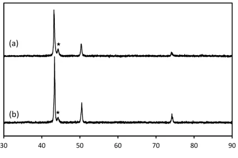
analysis of thermally and IPL sintered traces seen in Figure 3 (a and b) indicates that the reduction of Cu MOD ink to metallic Cu occurs without oxide formation. The small peak near the main peak of Cu located at 43°, for both the thermal and IPL sintered Cu traces is attributed to the polyimide substrate (Figure S4).
Printed Trace Characterization.
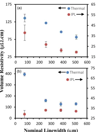
Figure 4 depicts the photographs of thermally sintered Cu traces on Kapton and PET. Printability was assessed using a test pattern that includes 10 cm long straight lines ranging from ~70 to 550 m width, bent traces, concentric circles and dots. The line width and thickness of the Cu traces were determined with (3D) optical profilometry. The dimensional and electrical properties of thermal and IPL sintered Cu traces on Kapton are summarized in Table 2. Volume resistivity of screen printed Cu traces as a function of nominal line width on Kapton are shown in Figure 5a. The optimized ink enables screen printed traces down to < 75 µm linewidth with good conductivity while still having long term oxidation stability. Based on Table 1 and the literature, this is not easily achieved when you consider 1) the rheology of the ink to be compatible with screen printing
2) have proper surface tension with the substrate to have good printability and 3) have the right chemistries to ensure that copper does not oxidize in the presence of oxygen during the sintering step. This last point is particularly interesting when printing high resolution traces as the surface area of fine lines increases with respect to the volume of the trace causing surface oxides to play a larger role in the electrical properties of the traces (i.e. fine lines often have poor conductivities due to oxidation as can be seen in Table 2). Though the print resolutions for the traces are similar, the thermally sintered traces are thicker (1.3 vs. 0.9 μm) and have resistivity values ~ 4 times higher than the traces processed via IPL sintering. Specifically, the sheet resistivity ranges ~8 to 15 m//mil (20-38 .cm) for the IPL sintered traces and 32-54 m//mil for the thermally sintered traces.
SEM analysis of the traces was carried out in order to understand how the different processing conditions impact the morphology and microstructure of the traces. As highlighted in Figure 6, traces that were dried at ~130C and thermally sintered at ~200C for 5 min followed by ~220C for 5 min are composed of large (500 nm - 1µm), granular particles that are randomly structured with poor physical contact between particles, resulting in higher resistivity values. For thermally sintered traces without a drying step, results are showing even higher resistivity values. This is consistent with SEM analysis that indicates traces with very large particles (1-3 µm) and large voids are produced (Figure S5), which is ascribed to the simultaneous evaporation of DEAPD and decomposition of Cu formate. In contrast, SEM analysis of the traces produced from IPL sintering suggest that the traces are porous, but composed of smaller and highly interconnected/bridged particles. It is interesting that, despite the porosity, the conductivity of the traces is very good, most likely due to the strong bridging of CuNP. IPL sintered Cu41,54 and Ag34 based MOD ink
high surface roughness and lower conductivity than the thermally sintered Ag traces, which was, in part, a function of the drying step before IPL sintering (residual solvent affects porosity).34 In
this study, the improved smoothness of Cu traces is the result of an optimized drying step prior to IPL sintering; Cu traces are dried at comparatively higher temperature ~125C for 20 minutes as oppose to our Ag MOD ink which is ~ 75C for 15 minutes. Recently, Ryu et al. studied IPL sintering of Cu nano/micro particles screen ink under vacuum stretching and heating of polymer substrate.55 Their results suggest that an appropriate substrate heating (150°C under vacuum)
contributed to the reduction of porosity i.e. dense structure with high conductivity and adhesion strength of Cu films.55 In essence, with IPL sintering, an optimized drying step is important to
control trace porosity. We see improved trace morphology with the Cu MOD ink using IPL vs thermal sintering. This translates into improved resistivity values, which are comparable to IPL sintered Ag MOD inks.34
Resistivity values of thermally and IPL sintered Cu traces produced using Cu MOD ink with and without CuNP and polyester binder are presented in Figure 7 and physical and electrical data is summarized in Table S2. Cu traces (~500-540 m wide) derived from Cu MOD ink without CuNP and binder produced higher volume resistivity values for thermal and IPL sintered traces ~206 .cm and ~60 .cm, respectively. Addition of CuNP (0.4 wt% to the total amount of ink) without binder decreased the volume resistivity for both thermal and IPL sintered traces to ~57 .cm and ~20 .cm respectively. Addition of a fractional amount of binder (0.3 wt% to the total amount of ink) without CuNP resulted in an increase in the volume resistivity of sintered traces for both thermal ~ 30% and IPL ~ 8% to ~266 .cm and ~65 .cm respectively. Addition of both CuNP and binder resulted in ~30% higher volume resistivity for thermally sintered traces (~ 80 .cm) whereas the resistivity of IPL sintered traces remained the same.
The impact of the addition of fractional amounts of CuNP and binder on the electrical properties of thermally and IPL sintered Cu traces can be rationalized by examining the morphology of the sintered traces as shown in Figure 6, providing mechanistic insight into both sintering processes. The optimized MOD ink consists of 0.4% of CuNP, which is 2.4% to the total amount of Cu in the ink. General observations that apply to both thermally and IPL sintered traces are that adding CuNPs lowers the resistivity. Adding binder in the absence of CuNPs increases resistivity, yet when CuNPs are included, the negative impact of the binder on resistivity is essentially negated, more so for the IPL sintered traces. However, as can be seen in the SEM images in Figure 6, the morphology is quite different for thermally and IPL sintered Cu traces, as such we will consider them separately.
For thermally sintered traces we observe relatively larger particles originating from the Cu complex (Fig 6 a-d). These larger particles impart a certain porosity to the trace due to poor inter-particle connectivity which results in relatively higher resistivity. When CuNPs are introduced (Fig 6b), the porosity of the film is visibly reduced as small clusters of CuNP can be seen bridging the larger particles, which would explain the improved resistivity. The addition of binder in the absence of CuNP (Fig 6c) combines both porosity and a non-conductive element which increases the resistivity, and morphologically it is similar to Fig 6a. Lastly, Fig 6d depicts the morphology of the optimized ink with CuNP and binder, where better film uniformity is observed macroscopically, and clusters of CuNPs are bridging larger particles, with binder interference being largely negated.
For IPL sintered traces the morphology is quite different, yet the impact of the CuNPs and binder follow a similar trend, albeit with superior electrical properties obtained with IPL sintering (See Figure 7). For IPL sintered traces, however, the mechanism by which Cu complex is converted to
metal happens extremely fast, on the order of milliseconds, compared to the thermal process, leading to a porous, albeit well connected network of nanoparticles, on the order of 100 nm in diameter, as can be seen in Fig 6e-h. The addition of CuNP is not discernable by SEM except to say that the porosity seems to be reduced at higher magnification. The CuNPs contribute positively to the electrical properties of the copper traces, while the polyester binder has a negative effect on the electrical properties but acts to enhance the mechanical properties of the traces. Even though the impact of binder is not evident in the trace morphology, for either sintering process, it does not seem to impede how the CuNP combine with the metal complex to form a copper trace (compare Fig 6b to 6d and 6f to 6h). However, the binder does provide superior mechanical performance and adhesion to the Cu traces for both thermal and IPL sintered traces without significantly affecting the conductivity of traces when CuNP are present, which is consistent with the SEM images. In fact, the effect of binder on the conductivity of IPL sintered traces is almost negligible due to excellent particle connectivity through welding as seen from the morphology. The unique synergistic benefits of CuNP and binder in the Cu traces is further supported by demonstration of direct solderability in the following section.
The Cu MOD ink was also printed on PET to explore the potential for the Cu MOD ink on a lower cost substrate. Table 3 summarizes the physical and electrical data. On PET, traces are either thermally sintered at 140C for an hour or dried at 100C for an hour before IPL sintering. The resistivity values on PET for both thermal as well as IPL sintered traces are 1.5 times greater than those on Kapton respectively (Figure 5b). The lowest volume resistivity ~130 .cm and ~32 .cm are obtained on PET for thermal and IPL sintered traces, respectively. The volume resistivity of our Cu MOD ink obtained on PET by IPL sintering is comparable with IPL sintered pure CuNP screen ink on PET ~44 .cm35, yet mechanical properties of CuNP screen ink were
lacking. While commercial Novacentrix CuO NP ink inkjet printed on silica coated PET (Novele) can produce ~10 .cm56,57, there is currently no screen printable formulation with adequate
mechanical properties and air stability of traces on conventional PET. Further comparisons include, Kawasaki et al. 15 where PET coated with Cu composite nano ink consisting of
submicron/nano-Cu particles with roller bar resulted volume resistivity of 50 .cm when sintered at 150C under N2. However, the screen printability of composite nano inks was not evaluated.
The volume resistivity of our Cu MOD ink obtained on PET by IPL sintering in air is also comparable with high Cu loaded hybrid inks (37 wt% Cu) that are doctor-blade coated on PET followed by either thermally sintering23 or flashlight sintering42 under N
2.
Mechanical robustness of these conductive traces is equally important for their use in various commercial applications. ASTM F1683-02 flex and crease testing was carried out on 10 cm long 70-550 m wide traces. In our recent study we demonstrated a Ag molecular ink with <10% change in the measured resistance of traces after mechanical testing.34 Meanwhile, Happonen et
al. in their recent work on screen printed silver traces used 20% change in the resistance as a failure criteria.58,59 IPL sintered traces on Kapton passed the flex and crease testing with <10% increase
in resistance without open fails (no loss of conductivity due to cracks or peel off) as shown in Table S3. On PET, resistance increase is < 20% except for the tensile flex (~24%) as shown in Table S4. It is noteworthy, that the excellent mechanical properties are obtained with very little polymer binder (0.30% to the total amount of ink). For thermally sintered traces, resistance increase after flex and crease testing on Kapton is < 20% except tensile flex (> 80%) and on PET 30% (Table S5 and S6). In addition, an adhesion tape test ( ASTM D3359), was carried out on thermally and IPL sintered Cu traces produced without binder on Kapton and PET yielded 0B to 1B level adhesion (Figure S6 a-d). On the other hand, addition of a fractional amount of binder
improved adhesion on thermally sintered Cu traces on Kapton and PET significantly to 5B and 4B level respectively. The same results were obtained for IPL sintered traces (Figure S6 e-f), indicating strong adhesion to the substrate. Hence, if adhesion is not the root cause, the relatively poorer mechanical performance for thermally sintered traces is likely due morphological differences i.e. due to larger Cu particles randomly joined forming the microstructure of the traces as observed by SEM. In the absence of polymer binder, >30% increase in the measured resistance was observed after flex and crease testing with several of open fails for both thermal and IPL sintered Cu traces on Kapton (Table S7) and PET. Other common binders such as ethyl cellulose, PVP and phenalloy 2870 were simply incompatible with the rest of the components leading to failed mechanical test even when used up to 2 wt%. This highlights the importance of carefully selecting all the components of the ink to not only render it printable, but to also yield relevant mechanical and electrical performance. In order to understand the role of the binder in obtaining optimized Cu films, we characterized IPL sintered Cu films on Kapton with and without binder using XPS, Raman and Fourier transform infrared spectroscopy (FTIR-ATR). Similar results were observed for thermally treated films.
Figure 8 presents the XPS spectra of IPL sintered Cu films with and without binder. The inset shows the Cu2p core level binding energy spectra. As XPS is a surface technique, the results show that the surfaces of the Cu particles in the film with binder have a higher relative concentration of carbon and lower relative concentration of Cu in the traces compared to those without (Figure 8). The 70 % decrease in the relative amount of Cu (Figure 8, inset) with double the amount of carbon in the traces with binder indicate the presence of the polymer binder coating on the Cu surface. These results are consistent with the fact that a fractional amount of polyester binder provides good passivation to the copper particles while enabling intimate inter-particle contact. It is interesting
to note that the polyester binder used in this study is a liquid at room temperature and it remains fluid when we carried out simple fluidity test in a reflow oven using the same thermal profile to sinter the copper traces (Figure S7). Reflow oven processing of binder, binder plus DEAD and binder plus Cu MOD complex confirm that it does not crosslink with either DEAPD or Cu MOD complex. In fact this inherent fluidity allows the binder to effectively coat the Cu surface at higher temperature and prevent oxidation. However, binders such as PEG and PVP form solid films under these conditions, which could lead to cracks, and poor passivation. Also, the TGA data of the polyester binder in Figure 1a shows the stability of the binder up to 250°C with negligible mass loss. Good thermal stability combined with the fluid nature of polymer binder under sintering conditions (~220°C) provides a means of stabilizing the Cu nanoparticles seeded in the trace upon decomposition of the complex. Keep in mind, TGA results show that DEAPD is released and the complex decomposes at ~ 150°C, which is confirmed visually due to the formation of Cu nanoparticles. At ~ 210-220°C, the fluid binder will play the role of stabilizing and passivating Cu nanoparticles as they grow and DEAPD is released from the film.
The presence of several moieties in the polymer may also explain why it is effective at oxidation resistance. The presence of COOH functional groups in the binder is confirmed by FTIR spectroscopy, as shown in Figure 9. The characteristic peak observed at 1724 cm-1 is attributed to
C=O stretching of the carboxyl ester group whereas the carboxylic OH group at 3450 cm-1.60 The
peak at 2872 cm−1 is ascribed to the C-H stretching vibrations of alkyl groups. These functional
groups cover the Cu nanoparticles and effectively block oxygen/water from reaching the particle surface, thus preventing oxidation. The use of carboxyl terminated polyester resin as a corrosion inhibitor for Cu has been reported in the literature.61 The role of the binder as an oxidation inhibitor
of the Cu film without binder depicts three characteristic peaks for Cu oxide at 147, 217 and 638 cm-1.62 These peaks are not observed in the Cu film with binder suggesting the binder used in this
study is not merely an adhesive but also acts as a stabilizer and an oxidation inhibitor. The amount of binder in the Cu film is relatively low (~2%) and therefore the characteristic peaks of the binder at 1460, 1658 and 1743 cm-1 are not observed in the Raman spectrum of the Cu film with binder.
The binder is also undetectable in sintered copper traces by FTIR.
The unique combination of Cu-MOD ink comprising Cu MOD precursor with fractional amount of CuNP and polymer binder not only produced conductive, mechanically robust traces with strong adhesion but also revealed practical shelf life. We examined the oxidation stability of the as-produced Cu traces (no passivation with a dielectric) and determined the resistance increases <10% over a month in air ambient temperature and relative humidity (RH) in the range of 10-70%. This is enough to provide practical handling of samples in production over the course of days to weeks. However, without CuNP and binder under the same storage conditions, the resistance of Cu traces increased ~ 200% over the same time period.
Demonstrations of utility of Cu MOD Ink.
Directly soldering functional elements to printed conductive tracks is an important aspect of fabrication and can be a challenge in printed electronics. Issues encountered while attempting to perform lead-free soldering include the rapid diffusion of the solderable metallic traces in the solder leading to insufficient wetting and the difficulty to produce solder joints on oxidized metallic coatings. Ideally, printed Cu traces would enable direct lead-free soldering. IPL sintered Cu traces described herein produce low resistivity values, excellent adhesion and mechanical properties, which are needed to absorb the temperature stress or mechanical shock during
soldering. Oxidation resistance and low surface roughness are also attributes that may enable direct soldering. To demonstrate the viability, we have investigated the solderability using a soldering gun on thermally sintered thick traces (>5 µm) and reflow soldering using SAC 305 paste on screen printed and IPL sintered thin Cu traces (<1 µm) obtained from Cu MOD ink. Soldering with heat gun is a simple way to compare to reflow soldering using SAC 305 paste. However, this method is inherently poorly controlled and can destroy thin Cu traces. Nonetheless, in this study, thicker (> 1.5 m) Cu traces prepared with the combination of Cu MOD precursor, CuNP and polymer binder withstand the high temperatures long enough without destruction as seen in Figure 11 a-d. Cu MOD inks that do not contain both the CuNP and binder could not be soldered. For Cu traces prepared with CuNP without polymer binder the solder destroy/damage the Cu trace due to poor mechanical strength. However, for traces prepared with polymer binder without CuNP, the solder does not wet or adhere to the surface, meaning no joint is formed. From these comparative experiments, it is clear that the both CuNP and polymer binder provides a surface finish that optimizes the wettability with the solder, while better controlling the kinetics leading to a good solder joint without simply dissolving away the Cu trace. SEM analysis in combination with EDS analysis of a successfully heat-gun soldered Cu thick trace produced with the ink comprising Cu MOD precursor, CuNP and polymer binder was carried out to understand both the wetting behavior and determine if evidence of an intermetallic compound layer could be found at the interface between the solder and the Cu trace (Figure 11 b-d). As shown in Figure 6a, an effective joint is formed without damaging the Cu film. Typically, a silver, gold or nickel interlayer is used to promote the wettability for lead free soldering on Cu substrate and it is remarkable that a good joint can be formed without it.63 The EDS analysis on the resolidified solder SAC 305 in areas of
relative proportions (96.5, 3.0 and 0.5%) that are expected based on its elemental composition (Figure 11c). EDS analyses of the Cu surface a distance away from the solder joint shows the presence of Cu only. However, at the interface of the resolidified solder, EDS analysis shows clearly the formation of an intermetallic compound layer between the solder and the Cu trace (Figure 11d). At the solder joint i.e. at the interface, Sn has diffused into the Cu trace where the proportion of Cu is higher than expected ~ 50 wt % as compared to the elemental composition of Cu in SAC 305 solder (Figure 11c). The soldered traces have good adhesion strength, withstanding a scotch tape adhesion test.
To demonstrate the quality of the soldering Cu traces, LEDs were soldered to screen printed and IPL sintered Cu traces using SAC 305 paste in a reflow-oven. The illumination intensity of LEDs remains constant without degradation during folding, bending and creasing of Cu traces including heating at 140°C for 3 hours in ambient air as seen in the Figure 11e. The Cu MOD ink formulation presented herein brings together a unique combination of features with two unexpected observations; shelf stability and solderability, neither of which is obtained if a single element in the formulation is removed i.e. binder, the NP or both. The polyester binder not only acts as an adhesive but also an oxidation barrier (see SEM in Figure 6d) that effectively shields traces from oxidation.
The Cu MOD ink was also evaluated as a candidate material for an HDTV antenna. The return losses (S11) measured as a function of frequency for screen printed and IPL sintered Cu antennas on Kapton and PET are depicted in Figure 12. Top section of graph shows the location (in frequency) of TV channels in the VHF-low, VHF-high and UHF bands. Antennas printed on Kapton and PET substrates produced similar performance in the UHF band (500-600 MHz). The minimum measured S11 was -12 dB and occurs at one of the resonance frequencies near 600 MHz.
Lower values of S11 indicate higher received power (higher probability of receiving a channel at its designated frequency). As per the literature, return loss of less than 10 dB indicates an acceptable sensitivity.64,65 Antennas on PET provided a better response in the upper VHF band.
The Cu MOD ink was also used to screen print source/drain electrodes in sc-SWCNT based TFTs. Bottom contact devices show greater variability and lower mobilities compared to top contacts, which is somewhat expected due to the presence of the binder providing oxidation stability to the contacts. Top contact devices made with either thermal or photo sintered contacts generally yield devices with mobilities in the range of 5-15 cm2/Vs and on/off ratios of 103-105,
however, thermally sintered contacts yield slightly higher mobilities than photo sintered contacts at a similar tube densities (determined by Raman scattering). The transfer characteristics for a representative TFT is shown in Figure 13. While the screen used to print this device had nominal dimensions of L=125 µm and W=250 µm, slight spreading of the ink led to a slightly smaller channel length of ~110 µm and wider width of 260 µm. The electrical characteristic of the device exhibit an on/off ratio in the range of 9.6 x 10⁴ (measured at V
ds=-1V). Linear fits to the transfer
curve above threshold yields a mobility value ~ 11.7 cm2/V-1s-1 (using the parallel plate model to
calculate the capacitance Cox= 34 nF/cm-2). These mobility values are comparable to our
previously reported results with screen printed silver electrodes34 and an order of magnitude higher
than inkjet printed CuNP ink electrodes used in the fabrication of organic66 and amorphous
semiconductor67 TFTs. Top contact devices were found to exhibit good atmospheric stability,
withstanding 150C annealing (20 minutes) in ambient conditions and remained operational after being exposed to air ambient conditions six months after fabrication (25-30C and 10-70% RH). Preliminary sensing response for ammonia using experimental conditions described previously68
The response time is as fast and comparable Au and Ag source-drain electrode based TFTs. These results suggest that the Cu MOD ink has potential for cost-effective flexible devices and sensors.
CONCLUSIONS
In summary, we formulated a screen-printable Cu ink comprising a MOD compound, conductive filler and binder to produce fine features that can be processed via thermal and IPL sintering. In addition to screen printability, the ink has demonstrated key features to realize commercial relevance, such as higher tolerance towards trace oxygen during sintering, good adhesion and mechanical robustness, as well as good electrical performance. The unique combination of polymer binder and CuNP was found to be necessary to obtain shelf-stability and direct solderability of screen printed Cu traces. This combination of attributes makes for a practical leap forward in Cu MOD ink formulation, which is further supported by the applications we have demonstrated, including bonded LEDs directly soldered to screen printed traces not requiring a precious metal interlayer, HDTV antennas that perform well in the UHF region and screen printed Cu source and drain electrodes in SWCNT-based TFTs that effectively sense ammonia in the ppb range while having excellent electrical characteristics (11.7 cm2 V-1 s-1 with current on/off ratio of
~105) even after 6 months exposure to air ambient conditions. For certain applications, such a Cu
Table 1. Optimization of Cu MOD screen ink. Amino alcohols1: aminomethyl propanol, amino butanol, dimethyl amino propanol, butyl amino ethanol; Alkyl amines2: Ethyl hexyl amine, octylamine; Amino diols3: 3-dimethylamino-1-2 propane diol, 3-methylamino propane diol and 3-morpholino-1-2-propane diol. PVB: poly(vinyl butyral), PVP: polyvinylpyrrolidone, PVA: poly(vinyl alcohol), PEG:polyethylene glycol. *Binder ≥2 wt % to total amount of ink.# Oxidation under 99.99% nitrogen with < 50 ppm oxygen.
Ink components Ink
Stability Ink Rheology Screen Printability Resolution 10 cm lines Oxidation of Cu traces during Sintering Resistance of 10 cm line Adhesion/ Mechanical Strength Solderability Cu MOD Ink + CuNP + Binder DEAPD + CuNP + Polyester Binder
Good Good Good Good Good Good Good
Cu MOD Ink with different amine ligands Amino alcohols1
Good Too low viscosity
No screen printing at all
Alkyl amines2 Good Good No Printing
≤ 127 µm width
#Oxidation ≤ 508 µm width <2µm thick lines
Amino diol3 Precipitation
Incompatible with binder No screen printing at all Wt% CuNP to the total amount of Cu in ink
2 - 3.6 wt% Good Good Good Good Good
(35-135 Ω) Failed test 0B-1B No solderability > 3.6 wt% Aggregation of CuNP Good No Printing ≤ 127 µm width Good Poor 500Ω-1KΩ Failed test 0B-1B Binder Polyester binder
Good Good Good Good Poor
≥ 300Ω Good No solderability Ethyl cellulose Hydroxyethyl cellulose PVB Poor Precipitation of ink No screen printing at all PVP* PVA* PEG* silane agents * phenalloy 2870*
Good Good Good #Oxidation ≤ 508 µm width <2µm thick lines Poor 1KΩ Failed test 0B-1B
Figure 1. (a) Thermogravimetric analysis of molecular Cu ink (blue line), DEAPD (orange line), polyester binder (green line) and anhydrous Cu formate (black line) and (b) Release of the amine ligand, CO2 and aldehyde as detected by TGA-FTIR (5C/min).
Temperature (C) N or m al iz ed A b so rb an ce 0.0 0.2 0.4 0.6 0.8 1.0 1.2 0 50 100 150 200 250 300 350 400 Ink-CO2 Ink_Amine Ink-Aldehyde DEAPD-Amine (b) W ei gh t L os s (% ) -20 -15 -10 -5 0 5 0 20 40 60 80 100 120 0 50 100 150 200 250 300 350 400 Molecular Cu ink-TGA DEAPD_TGA Polyester binder-TGA CuF anhyd-TGA Molecular Cu ink-DTGA DEAPD-DTGA Polyester binder CuF anhyd-DTGA d m /d t ( % m in ) (a)
Figure 2. (a) Effect of drying temperatures on sheet resistivity and (b) dependence of sintering energies on sheet resistivity of screen printed ~500 m traces dried at ~120C for 20 min on Kapton. Drying Temperature (C) S h ee t R es is ti vi ty ( m / /m il ) Sintering Energy (J/cm2) 0 10 20 30 40 50 60 90 100 110 120 130 140 2.68 J/cm 2.94 J/cm 3.1 J/cm S h ee t R es is ti vi ty ( m / /m il ) 0 5 10 15 20 2.2 2.4 2.6 2.8 3 3.2 (a) 22 (b) 2
Figure 3. XRD pattern of (a) thermal and (b) IPL sintered Cu traces. The small peak* attributed to the substrate Kapton.
Cu (200) Cu (220) Cu (111) 2 Theta In te n si ty 30 40 50 60 70 80 90 (a) (b)
Figure 4. Photographs of thermally sintered Cu traces on (a) Kapton and (b) PET produced from screen printing of MOD ink. Test pattern comprised of 10 cm long straight line ranging from ~ 70 – 550 µm width, bent traces, concentric circle and dots is shown on PET (b). The 3D optical profilometry images of concentric circle, dots and lines are shown in (c), (d) and (e), respectively.
(a) (b)
Table 2. Comparison of physical and electrical data for linear 10 cm screen printed traces thermally and IPL sintered Cu molecular ink on Kapton™
Sintering
Method Nominal Linewidth (m) Measured Linewidth (m) Resistance () Sheet Resistance (m/) Trace thickness (m) Sheet Resistivity (m//mil) Volume Resistivity (.cm) Thermal 50.8 73 ± 3.9 4200 ± 230 3127 ± 332 0.44 ± 0.01 53.7 ± 4.3 136 ± 11 Photonic 69 ± 0.8 2627 ± 572 1980 ± 0.24 0.19 ± 0.06 14.96 ± 2.9 38.0 ± 7.4 Thermal 127 145 ± 14 942 ± 61 1364 ± 127 0.9 ± 0.1 48.2 ±0.9 122 ± 2.3 Photonic 167 ± 1.3 437 ± 36 789 ± 0.11 0.34 ± 0.01 10.6 ± 1.1 26.8 ± 2.8 Thermal 381 384 ± 17 176 ± 34 670 ± 106 1.46 ± 0.25 38.0 ± 0.8 96.6 ± 2.1 Photonic 411 ± 6.2 54.4 ± 2.2 232 ± 0.02 0.92 ± 0.01 8.39 ± 0.7 21.3 ± 1.7 Thermal 508 507 ± 16 123 ± 18 625 ± 92 1.31 ± 0.09 32.1 ± 2.3 81.5± 6.1 Photonic 545 ± 5.9 38.1 ± 1.7 213 ± 0.01 0.92 ± 0.05 7.69 ± 0.39 19.55 ± 1
Figure 5. Volume resistivity of screen printed Cu traces as a function of nominal line width. Cu molecular ink thermally and IPL sintered on (a) Kapton and (b) PET.
15 25 35 45 55 65 25 75 125 175 0 100 200 300 400 500 600 Thermal IPL 25 35 45 55 65 75 0 100 200 300 400 0 100 200 300 400 500 600 Thermal IPL Nominal Linewidth (m) V ol u m e R es is ti vi ty ( .c m ) (a) (b)
Figure 6. SEM of screen printed and thermally sintered (a-d) and IPL (e-h) sintered Cu traces on Kapton prepared from ink without and with CuNP and binder.
T he rm al 1 µm Cu MOD Ink 1 µm 1 µm 2 µm IP L
Cu MOD Ink + CuNP Cu MOD Ink + Binder Cu MOD Ink + CuNP + Binder
250 nm 250 nm 250 nm 250 nm b c d a f g h e
Figure 7. Volume resistivity bar charts of Cu traces produced using Cu MOD ink with and without binder. 0 50 100 150 200 250 300 Thermal Sintering
Cu MOD Cu MOD + CuNP
Cu MOD + Binder Cu MOD + CuNP+ Binder
0 10 20 30 40 50 60 70 80 IPL Sintering
Cu MOD Cu MOD + CuNP
Cu MOD + Binder Cu MOD + CuNP+ Binder
Vo lu m e Re si st iv ity (µ Ω .c m )
Table 3. Comparison of physical and electrical data for linear 10 cm screen printed traces thermally and IPL sintered Cu molecular ink on PET.
Sintering
Method Nominal Linewidth (m) Measured Linewidth (m) Resistance () Sheet Resistance (m/) Trace thickness (m) Sheet Resistivity (m//mil) Volume Resistivity (.cm) Thermal 76.2 102 ± 1.3 5100 ± 326 5242 ± 381 0.76 ± 0.05 156 ± 5.8 395 ± 15 Photonic 77 ± 2.8 1111.5 ± 0.7 856 ± 31 0.33 ± 0.03 12 ± 1.4 29 ± 3.8 Thermal 254 266 ± 7.1 414 ± 19 1103 ± 67 1.45 ±0.1 63 ± 5.1 159 ± 12 Photonic 240 ± 1.4 183.5 ± 2.1 440 ± 7 0.75 ± 0.01 13 ± 0.4 33 ± 0.9 Thermal 381 378 ± 23 228 ± 27 863 ± 130 1.48 ± 0.05 50 ± 6.7 127 ± 17 Photonic 360.5 ± 0.7 102 ± 2.8 367 ± 11 0.91 ± 0.1 13 ± 0.5 33 ± 1.3 Thermal 508 493 ± 22 158 ± 19 782 ± 113 1.68 ± 0.14 51 ± 4.1 129 ± 11 Photonic 467 ± 5.6 75.5 ± 2.1 352 ± 14 0.91 ± 0.1 12.5 ± 0.2 32 ± 0.5
Figure 8. X-ray photoelectron spectroscopy (XPS) survey spectra of IPL sintered Cu film with and without binder. The inset shows the Cu2p core level binding energy spectra.
Binding Energy (eV)
200 400 600 800 1000
C
o
un
ts
BE (eV) 930 935 940 945 950 955 960 Cu2p Cu2p C1s CuLMM O1s binder no binderFigure 9. FTIR spectrum of carboxyl terminated polyester resin binder. FTIR spectrum was taken using Agilent Cary 630 FTIR spectrometer.
500 1000 1500 2000 2500 3000 3500 4000 Wavenumbers (cm-1) 1724 1473 1178 1376 1025 2966 3450 2872
Figure 10. Raman spectra of binder (carboxyl terminated polyester resin), Cu film without binder and Cu film with binder. The small peak* are attributed to the glass substrate.
100 300 500 700 900 1100 1300 1500 1700 1900 Cu without binder Cu with binder binder Raman Shift (cm-1) 638 217 147 * * 1460 1658 1743
Figure 11. Characterization of directly soldered thick Cu trace using soldering gun and reflow soldering of thin Cu trace using SAC 305 paste. Directly soldered Cu thick trace (>5 µm) were blade coated and thermally sintered (a-d): (a) SEM images of directly soldered copper trace, (b) SEM cross section of soldered Cu trace (spectrum boxes show the layers of scanning), (c) EDS analysis of solder on the Cu traces, (d) EDS layered analysis of soldered Cu interface and (e) photographs of functional LEDs bound to the screen printed and IPL sintered thin Cu trace (< 1µm) by reflow soldering using SAC 305 paste.
0 20 40 60 80 100 33 34 35 36 37 38 Sn Cu Ag Layers # % M et al Cu Solder (a) (c) (b) (d)
Figure 13. Transfer curve of an arc-PFDD/SWCNT TFT fabricated on a SiO2(100 nm) /Si substrate with Cu source drain contacts screened printed on top of the SWCNT network and thermally sintered. The device dimensions were measured to be (L= 110 µm, W= 260 µm), indicating some spreading from the mask dimensions (125 x 250 µm).
AUTHOR INFORMATION Corresponding Author
*E-mail: Bhavana.deore@nrc-cnrc.gc.ca; Patrick.Malenfant@nrc-cnrc.gc.ca
ACKNOWLEDGMENT
We thank David Kingston SEM analysis, Katie Sampson for Raman analysis and Malgosia Daroszewska TGA analysis.
Supporting Information. Additional ink characterization data, as well as electrical, morphological, and mechanical data
REFERENCES
(1) Sarobol, P.; Cook, A.; Clem, P. G.; Keicher, D.; Hirschfeld, D.; Hall, A. C.; Bell, N. S. Additive Manufacturing of Hybrid Circuits. Annu. Rev. Mater. Res. 2016, 46 (1), 41–62. (2) Wu, W. Inorganic Nanomaterials for Printed Electronics: A Review. Nanoscale 2017, 9
(22), 7342–7372.
(3) Nathan, A.; Ahnood, A.; Cole, M. T.; Lee, S.; Suzuki, Y.; Hiralal, P.; Bonaccorso, F.; Hasan, T.; Garcia-Gancedo, L.; Dyadyusha, A.; Haque, S.; Andrew, P.; Hofmann, S.; Moultrie, J.; Chu, D.; Flewitt, A.J.; Ferrari, A. C.; Kelly, M. J.; Robertson, J.; Amaratunga, G. A. J.;Milne, W. I. Flexible Electronics: The next Ubiquitous Platform. Proc. IEEE 2012, 100 (SPL CONTENT), 1486–1517.
(4) Homenick, C. M.; James, R.; Lopinski, G. P.; Dunford, J.; Sun, J.; Park, H.; Jung, Y.; Cho, G.; Malenfant, P. R. L. Fully Printed and Encapsulated SWCNT-Based Thin Film Transistors via a Combination of R2R Gravure and Inkjet Printing. ACS Appl. Mater. Interfaces 2016, 8 (41), 27900–27910.
(5) Sung, D.; De La Fuente Vornbrock, A.; Subramanian, V. Scaling and Optimization of Gravure-Printed Silver Nanoparticle Lines for Printed Electronics. IEEE Trans. Components Packag. Technol. 2010, 33 (1), 105–114.
(6) Hong, K.; Kim, S. H.; Mahajan, A.; Frisbie, C. D. Aerosol Jet Printed P- and n-Type Electrolyte-Gated Transistors with a Variety of Electrode Materials: Exploring Practical Routes to Printed Electronics. ACS Appl. Mater. Interfaces 2014, 6 (21), 18704–18711. (7) Kamyshny, A.; Magdassi, S. Conductive Nanomaterials for Printed Electronics. Small
2014, 10 (17), 3515–3535.
(8) Wünscher, S.; Abbel, R.; Perelaer, J.; Schubert, U. S. Progress of Alternative Sintering Approaches of Inkjet-Printed Metal Inks and Their Application for Manufacturing of Flexible Electronic Devices. J. Mater. Chem. C 2014, 2 (48), 10232–10261.
(9) Salmerón, J. F.; Molina-Lopez, F.; Briand, D.; Ruan, J. J.; Rivadeneyra, A.; Carvajal, M. A.; Capitán-Vallvey, L. F.; De Rooij, N. F.; Palma, A. J. Properties and Printability of Inkjet and Screen-Printed Silver Patterns for RFID Antennas. J. Electron. Mater. 2014, 43 (2), 604–617.
(10) Ostfeld, A. E.; Deckman, I.; Gaikwad, A. M.; Lochner, C. M.; Arias, A. C. Screen Printed Passive Components for Flexible Power Electronics. Sci. Rep. 2015, 5 (1), 15959.
(11) Hermerschmidt, F.; Burmeister, D.; Ligorio, G.; Pozov, S. M.; Ward, R.; Choulis, S. A.; List-Kratochvil, E. J. W. Truly Low Temperature Sintering of Printed Copper Ink Using Formic Acid. Adv. Mater. Technol. 2018, 1800146, 1–6.
(12) Deng, D.; Jin, Y.; Cheng, Y.; Qi, T.; Xiao, F. Copper Nanoparticles: Aqueous Phase Synthesis and Conductive Films Fabrication at Low Sintering Temperature. ACS Appl. Mater. Interfaces 2013, 5 (9), 3839–3846.
(13) Magdassi, S.; Grouchko, M.; Kamyshny, A. Copper Nanoparticles for Printed Electronics: Routes towards Achieving Oxidation Stability. Materials (Basel). 2010, 3 (9), 4626–4638. (14) Kanzaki, M.; Kawaguchi, Y.; Kawasaki, H. Fabrication of Conductive Copper Films on Flexible Polymer Substrates by Low-Temperature Sintering of Composite Cu Ink in Air. ACS Appl. Mater. Interfaces 2017, 9 (24), 20852–20858.
(15) Akiyama, Y.; Sugiyama, T.; Kawasaki, H. Contribution of Ligand Oxidation Products to High Durability of Copper Films Prepared from Low-Sintering-Temperature Copper Ink on Polymer Substrates. Adv. Eng. Mater. 2017, 19 (8), 1–8.
(16) Farraj, Y.; Smooha, A.; Kamyshny, A.; Magdassi, S. Plasma-Induced Decomposition of Copper Complex Ink for the Formation of Highly Conductive Copper Tracks on Heat-Sensitive Substrates. ACS Appl. Mater. Interfaces 2017, 9 (10), 8766–8773.
(17) Choi, Y. H.; Hong, S. H. Effect of the Amine Concentration on Phase Evolution and Densification in Printed Films Using Cu(II) Complex Ink. Langmuir 2015, 31 (29), 8101– 8110.
(18) Shin, D.-H.; Woo, S.; Yem, H.; Cha, M.; Cho, S.; Kang, M.; Jeong, S.; Kim, Y.; Kang, K.; Piao, Y. A Self-Reducible and Alcohol-Soluble Copper-Based Metal–Organic Decomposition Ink for Printed Electronics. ACS Appl. Mater. Interfaces 2014, 6 (5), 3312– 3319.
(19) Huang, K.-M.; Tsukamoto, H.; Yong, Y.; Chiu, H.-L.; Nguyen, M. T.; Yonezawa, T.; Liao, Y.-C. Stabilization of the Thermal Decomposition Process of Self-Reducible Copper Ion Ink for Direct Printed Conductive Patterns. RSC Adv. 2017, 7 (40), 25095–25100.
(20) Lee, J.; Lee, B.; Jeong, S.; Kim, Y.; Lee, M. Enhanced Surface Coverage and Conductivity of Cu Complex Ink-Coated Films by Laser Sintering. Thin Solid Films 2014, 564, 264–268.
(21) Cho, S.; Yin, Z.; Ahn, Y.; Piao, Y.; Yoo, J.; Kim, Y. S. Self-Reducible Copper Ion Complex Ink for Air Sinterable Conductive Electrodes. J. Mater. Chem. C 2016, 4 (45), 10740– 10746.
(22) Lee, B.; Jeong, S.; Kim, Y.; Jeong, I.; Woo, K.; Moon, J. Hybrid Copper Complex-Derived Conductive Patterns Printed on Polyimide Substrates. Met. Mater. Int. 2012, 18 (3), 493– 498.
(23) Li, W.; Cong, S.; Jiu, J.; Nagao, S.; Suganuma, K. Self-Reducible Copper Inks Composed of Copper–amino Complexes and Preset Submicron Copper Seeds for Thick Conductive Patterns on a Flexible Substrate. J. Mater. Chem. C 2016, 93, 1265–1272.
(24) Yonezawa, T.; Tsukamoto, H.; Yong, Y.; Nguyen, M. T.; Matsubara, M.; Moon, J.; Jeong, S.; Kim, Y.; Kang, K.; Piao, Y. Low Temperature Sintering Process of Copper Fine Particles under Nitrogen Gas Flow with Cu 2+ -Alkanolamine Metallacycle Compounds for
Electrically Conductive Layer Formation. RSC Adv. 2016, 6 (15), 12048–12052.
(25) Kawaguchi, Y.; Hotta, Y.; Kawasaki, H. Cu-Based Composite Inks of a Self-Reductive Cu Complex with Cu Flakes for the Production of Conductive Cu Films on Cellulose Paper. Mater. Chem. Phys. 2017, 197, 87–93.
(26) Rosen, Y. S.; Yakushenko, A.; Offenhäusser, A.; Magdassi, S. Self-Reducing Copper Precursor Inks and Photonic Additive Yield Conductive Patterns under Intense Pulsed Light. ACS Omega 2017, 2 (2), 573–581.
(27) Tam, S. K.; Fung, K. Y.; Ng, K. M. High Copper Loading Metal Organic Decomposition Paste for Printed Electronics. J. Mater. Sci. 2017, 52 (10), 5617–5625.
(28) Paquet, C.; Lacelle, T.; Liu, X.; Deore, B.; Kell, A. J.; Lafrenière, S.; Malenfant, P. R. L. The Role of Amine Ligands in Governing Film Morphology and Electrical Properties of