Publisher’s version / Version de l'éditeur:
ACS Nano, 11, 9, pp. 8636-8642, 2017-07-18
READ THESE TERMS AND CONDITIONS CAREFULLY BEFORE USING THIS WEBSITE. https://nrc-publications.canada.ca/eng/copyright
Vous avez des questions? Nous pouvons vous aider. Pour communiquer directement avec un auteur, consultez la
première page de la revue dans laquelle son article a été publié afin de trouver ses coordonnées. Si vous n’arrivez pas à les repérer, communiquez avec nous à PublicationsArchive-ArchivesPublications@nrc-cnrc.gc.ca.
Questions? Contact the NRC Publications Archive team at
PublicationsArchive-ArchivesPublications@nrc-cnrc.gc.ca. If you wish to email the authors directly, please see the first page of the publication for their contact information.
NRC Publications Archive
Archives des publications du CNRC
This publication could be one of several versions: author’s original, accepted manuscript or the publisher’s version. / La version de cette publication peut être l’une des suivantes : la version prépublication de l’auteur, la version acceptée du manuscrit ou la version de l’éditeur.
For the publisher’s version, please access the DOI link below./ Pour consulter la version de l’éditeur, utilisez le lien DOI ci-dessous.
https://doi.org/10.1021/acsnano.7b04238
Access and use of this website and the material on it are subject to the Terms and Conditions set forth at
Atomic white-out: enabling atomic circuitry through mechanically
induced bonding of single hydrogen atoms to a silicon surface
Huff, Taleana R.; Labidi, Hatem; Rashidi, Mohammad; Koleini, Mohammad;
Achal, Roshan; Salomons, Mark H.; Wolkow, Robert A.
https://publications-cnrc.canada.ca/fra/droits
L’accès à ce site Web et l’utilisation de son contenu sont assujettis aux conditions présentées dans le site LISEZ CES CONDITIONS ATTENTIVEMENT AVANT D’UTILISER CE SITE WEB.
NRC Publications Record / Notice d'Archives des publications de CNRC:
https://nrc-publications.canada.ca/eng/view/object/?id=dab42061-686c-4973-9e25-a7ae29497615 https://publications-cnrc.canada.ca/fra/voir/objet/?id=dab42061-686c-4973-9e25-a7ae29497615
Atomic White-Out: Enabling Atomic Circuitry
through Mechanically Induced Bonding of
Single Hydrogen Atoms to a Silicon Surface
Taleana R. Huff,*
,†,‡,⊥Hatem Labidi,
†,§,⊥Mohammad Rashidi,
†,§Mohammad Koleini,
†,§Roshan Achal,
†,‡Mark H. Salomons,
‡,§and Robert A. Wolkow*
,†,‡,§†
Department of Physics, University of Alberta, Edmonton, Alberta T6G 2E1, Canada
‡
Quantum Silicon, Inc., Edmonton, Alberta T6G 2M9, Canada
§
National Institute for Nanotechnology, National Research Council of Canada, Edmonton, Alberta T6G 2M9, Canada
*
S Supporting InformationABSTRACT: We report the mechanically induced formation of a silicon−hydrogen covalent bond and its application in engineering nanoelectronic devices. We show that using the tip of a noncontact atomic force microscope (NC-AFM), a single hydrogen atom could be vertically manipulated. When applying a localized electronic excitation, a single hydrogen atom is desorbed from the hydrogen-passivated surface and can be transferred to the tip apex, as evidenced from a unique signature in frequency shift curves. In the absence of tunnel electrons and electric field in the scanning probe microscope junction at 0 V, the hydrogen atom at the tip apex is brought very close to a silicon dangling bond, inducing the mechanical
formation of a silicon−hydrogen covalent bond and the passivation of the dangling bond. The functionalized tip was used to characterize silicon dangling bonds on the hydrogen−silicon surface, which was shown to enhance the scanning tunneling microscope contrast, and allowed NC-AFM imaging with atomic and chemical bond contrasts. Through examples, we show the importance of this atomic-scale mechanical manipulation technique in the engineering of the emerging technology of on-surface dangling bond based nanoelectronic devices.
KEYWORDS: mechanochemistry, silicon, dangling bonds, AFM, nanostructures, nanofabrication, nanolithography
D
ue to the continuous improvement of scanning probe microscopy techniques, the long thought inaccessible goal of inducing and visualizing chemical reactions at the atomic scale is now routinely achievable by many groups around the world. In the framework of so-called mechano-chemistry,1 mechanical force induced reactions have been studied using noncontact atomic force microscopy (NC-AFM).2 Recent works reported force-induced atomic-scale switching,3 quantitative force measurements to induce the diffusion of single atoms4 and molecules,5 and studyingmolecular conformers6 and tautomerization.7 A few earlier studies also showed examples of mechanically induced vertical manipulation of single atoms.8,9However, direct observation of mechanically induced covalent bonding of two different atoms using NC-AFM remains scarce.10
Recently, the silicon dangling bond (DB) on the technologically relevant H−Si(100) surface was established as a very promising building block for beyond CMOS technology.11,12 A DB corresponds to a desorbed single hydrogen atom from the otherwise passivated silicon surface. It is approximately an sp3hybrid orbital that can be occupied by
2, 1, or 0 electrons, resulting, respectively, in a negative, neutral, or positively charged DB. Thus, a DB behaves essentially as a
single-atom quantum dot, with charge state transitions reported in scanning tunneling microscope (STM) experiments.13,14
DBs can be found natively on the surface as a result of imperfections during the hydrogen termination procedure or artificially created using the STM tip. Different works have shown that controlled atom-by-atom lithography, i.e., hydrogen desorption, on the H−Si surface allows creation of DB-based circuits for next-generation ultimately miniaturized low-power nanoelectronic devices.11,12,15−17
Although STM tip induced desorption of hydrogen from the H−Si(100) surface was extensively studied,16,18−23the reverse
manipulation of selective adsorption of a single hydrogen atom to passivate a silicon DB has not been as rigorously examined.24
In this context, AFM can bring more insights by allowing identification of different tip dynamics25,26 and probing
chemical reactivity at the atomic scale.27,28
Here, we report the controlled vertical manipulation of a single H atom using the tip of an AFM sensor and its
Received: June 16, 2017 Accepted: July 18, 2017 Published: July 18, 2017
Article
application in characterizing and engineering silicon DB-based structures of relevance to nanoelectronic devices. We show that following a localized tip induced excitation on the Si−H surface, a single hydrogen atom is desorbed and could be either deposited on the surface with stable imaging in STM and AFM or transferred to the tip apex. The single H atom functionalized tip was identified through a unique signature in frequency shift
vs displacement curves (i.e., Δf(z)) and a characteristic
enhancement of STM images in filled and empty states. By bringing the H-functionalized tip apex very close to a DB in the absence of bias and current, a covalent bond between the single hydrogen and silicon atoms is formed. Subsequent changes in the STM images and Δf(z) curves confirmed that this mechanically induced reaction results in the passivation of the DB with the hydrogen from the tip apex.
It has become clear that CO-functionalized tips are effective for characterization of adsorbed molecules on metal surfa-ces.25,29 It is clear also that accessible and effective tips are required for other systems of study. Preparing and identifying such a tip is described in this work. Moreover, the H-functionalized tip is shown to allow characterization and also induce changes in DB-based structures on the H−Si(100) surface through selective mechanically induced hydrogen passivation, or “capping”.
RESULTS AND DISCUSSION
Tip Functionalization with a Single Hydrogen Atom. In the Si(100)-2×1 reconstruction, silicon atoms at the surface are organized in dimers. When the surface is passivated with hydrogen in the monohydride reconstruction, each silicon atom at the surface is covalently bonded with a single hydrogen atom as represented inFigure 1a.Figure 1b shows a typical defect-free empty state STM image acquired using a nonfunctionalized tip (see mMethods and ref 30 for details on in situ tip preparation).
Figure 1c shows a 3D ball-and-stick model of a silicon
dangling bond (represented in green) on the H−Si(100) surface. To create a single DB, the STM tip is positioned on top of a hydrogen atom (red dot inFigure 1b); then the feedback loop is switched off, and a voltage pulse of about 2.3 V is applied for a few milliseconds. As illustrated inFigure 1c, this results in the selective desorption of the hydrogen atom under the tip apex, which is often transferred to the tip. Figure 1d shows a typical STM image of the created single DB. In accordance with earlier studies in the literature, the DB in empty states appears as a bright protrusion surrounded by a characteristic dark halo.11,14
While the tip-induced desorption of hydrogen from the H− Si(100) surface has been studied by researchers for over two decades (see ref 14 for details), the location and mode of attachment of the H atom after desorption has remained rarely studied.31 Following procedures described here and tracking desorption events for several different tips, we found that DB creation through a voltage pulse resulted in the desorbed H atom being transferred to the tip apex roughly 50% of the time,
i.e., forming a H-functionalized tip. In 30% of cases, the
desorbed H atom is found on the H−Si surface close to the just created DB, as shown in Figure 2a, agreeing with similarly reported values of H returning to the surface in a study done by Ballard et al.31In the remaining 20% of cases, the tip apex does not change and a hydrogen atom could not be seen in the vicinity of the newly created DB, suggesting it was possibly
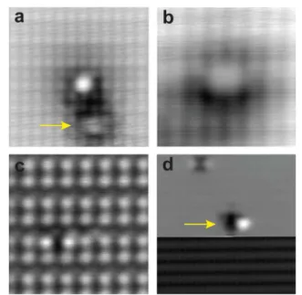
Figure 1. Illustration of the tip-induced manipulation that can result in tip functionalization with a single hydrogen atom. (a) Ball-and-stick model of the H−Si(100)-2×1 surface. (b) Typical defect-free empty state STM image using a nonfunctionalized tip and showing the dimer structure of the surface. The red dot indicates the position of the STM tip when the electronic excitation sketched in (a) is applied. (c) Ball-and-stick model of a silicon atom with a dangling bond in green and a H-functionalized tip resulting from the tip-induced desorption. (d) Typical STM image of a DB acquired with a H-functionalized tip showing a characteristic STM contrast enhancement. Both STM images were acquired in constant current mode with a set point of 50 pA at +1.3 V.
Figure 2. Imaging a single hydrogen atom physisorbed on the H− Si(100) surface. (a) A 5 × 5 nm2STM image at +1.3 V of a DB
where the desorbed atomic hydrogen was not picked up, instead adsorbing at the location indicated by an arrow. (b) 3 × 3 nm2
STM image of an atomic hydrogen adsorbed on the surface and (c) corresponding AFM frequency shift map at 0 V and a relative tip elevation of z = −3.8 Å. (d) An atomic hydrogen on the surface is picked up by a slow downward STM scan at V = +1.6 V. All STM images are constant current at 50 pA.
ACS Nano Article
DOI:10.1021/acsnano.7b04238
ACS Nano2017, 11, 8636−8642
adsorbed on the tip away from the apex atom, deposited on the surface farther from the DB, or ejected to the vacuum.
Figure 2a shows an example of a single hydrogen atom found
to be deposited on the H−Si surface immediately after tip-induced creation of a DB. Such an object was confirmed to be a single hydrogen atom by dragging it with an elevated positive bias to passivate the created nearby DB (Supporting
Information, Figure S1). Interestingly, the hydrogen atom
appears in empty state STM images as a slightly bright protrusion surrounded by a dark halo, as shown inFigure 2b. This suggests a possible charging effect that induces a localized band bending similar to a single DB.14,16In the corresponding frequency shift map (Figure 2c), the physisorbed hydrogen atom appears to induce a lattice distortion of two adjacent dimer pairs. We note here that the mismatch in the position of the physisorbed H atom between STM and AFM images is due to the diffusion of the H atom triggered by the ramping down of the bias when switching the scanning mode. When imaged at relatively high positive voltage (+1.6 V in the example ofFigure 2d), the hydrogen atom was picked up by the tip apex, as evidenced from the change in STM contrast midway through the scan.
In the examples of Figures 1 and 2, the enhanced STM contrast after creating a DB is a first strong indication of tip functionalization with the desorbed single H atom. The contrast changes from resolving dimers (Figure 1b) to resolving single atoms (Figure 1d), respectively, before and after the hydrogen desorption from the surface. This is similar to what is well known for the CO molecule, where once it is picked up by the tip apex following a voltage pulse it enhances the STM and AFM contrast.25,32,33 In the following section, we provide further evidence of a single hydrogen atom functionalized tip using NC-AFM, which allows identification of different tip dynamics through studying force curves.26,30,34
Mechanically Induced Covalent Bonding of Single Hydrogen and Silicon Atoms.Figure 3a shows a filled-state STM image of the H−Si surface with a silicon DB created using the procedure described in the previous section. Similar to the case of empty states, we notice an enhanced STM contrast. In fact, typical filled-state STM images of the H−Si surface usually show only dimer rows,14but inFigure 3a the dimers of dimer rows are clearly resolved.
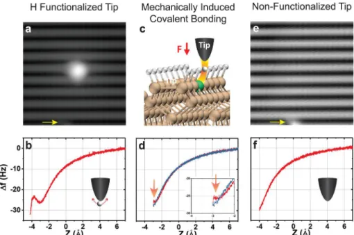
Following the creation of the single DB in Figure 3a, the scanner was switched to AFM scanning mode.Figure 3b shows a frequency shift vs displacement curve recorded using a hydrogen-functionalized tip on top of a hydrogen atom on the surface. The minima at around −3 Å is always seen when a functionalized tip is prepared following the procedure previously described. Such features were reported by other works in the case of functionalized tips and are ascribed to the relaxation of the functionalizing atom at the tip apex.7,29,35
When recorded on a DB using the same functionalized tip, Δf(z) curves exhibit a hysteresis between the forward and backward sweep when the tip is brought very close to the DB, as shown inFigure 3c and d, which indicates a change in the AFM junction.10,35,36 When acquiring a subsequent STM image, we notice that the DB was capped with a hydrogen atom. The defect indicated by the yellow arrow is used as a marker showing thatFigure 2e is exactly the same area as2a. Additionally, Δf(z) curves recorded on top of a hydrogen atom on the surface as shown in Figure 3f no longer exhibit the minima characteristic of the hydrogen-functionalized tip. This unambiguously proves that the tip that yields the minima in force curves was indeed functionalized with a single hydrogen atom.
Throughout all our experimental data, we saw that a tip that produces enhanced STM also systematically produces the characteristic force curves with the shallow minima. Therefore, a change in the STM contrast, such as presented inFigures 1d,
Figure 3. Procedure to mechanically induce a hydrogen−silicon covalent bond. (a) Typical filled-state STM image of a silicon dangling bond on the H−Si(100)-2×1 surface using a single hydrogen atom functionalized tip. The yellow arrow indicates a defect taken as a reference. (b) Δf(z) curve using a H-functionalized tip on a surface hydrogen atom. (c) Ball-and-stick model and (d) Δf(z) curve on a single DB during the mechanically induced Si−H covalent bond capping event. The orange arrow indicates a hysteresis (zoom in inset) characteristic of the change that occurs due to the formation of the covalent bond between the H atom at the tip apex and the silicon dangling bond. (e) STM image and (f) Δf(z) curve on the H−Si surface subsequent to the mechanically induced reaction in (d).
2a, and3a, indicates successful functionalization of the tip apex with a single hydrogen atom. This is important for technological applications related to altering DB engineered structures through capping, as a change in STM contrast to detect H-functionalized tips is a much faster indicator than the time-consuming acquisition of Δf(z) curves. In fact, regular systematic, non-tip-damaging, and reliable capping was produced using STM contrast as an indicator alone.
All Δf(z) curves were recorded at 0 V in the complete absence of tunnel current, and the hydrogen capping of the DB occurs only when the tip is brought to a close enough interaction distance. Therefore, the silicon−hydrogen covalent bonding is mechanically induced. We note here that mechanically induced desorption was also observed, but often resulted in tip structure changes or multiple hydrogens desorbed, unlike the gentle and precise tip-induced desorption. We note here that the initial tip apex structure before picking up a hydrogen atom on the tip apex is never exactly the same. So, the H−tip bond is not necessarily the same in all H-functionalized tips, similarly to the case of CO tips. This is likely the reason we observe variation on the tip elevation to induce capping. Other factors such as the sensor oscillation amplitude or the Δf(z) acquisition parameters might also play a role.
So far, reliable functionalization of tips mainly with CO molecules allowed different groups to achieve submolecular and bond contrast imaging of different molecular systems.25,29 In the following, we show that in addition to high-resolution AFM imaging H-functionalized tips can be implemented in atom-by-atom lithography to create and modify silicon DB based nanoelectronic elements.
Characterizing Silicon Dangling Bonds on the Si−H Surface with a H-Functionalized Tip.Although DBs on the H−Si surface have been extensively studied using STM, NC-AFM works remain almost nonexistent. NC-AFM can provide an important complementary view to STM works, as it allows characterizing the chemical reactivity of DBs. Moreover, unlike STM, AFM allows probing the electronic properties of DBs and DB structures in the band gap with minimized perturbation from the tip, e.g., minimal tip-induced band bending and electron/hole injection.14,15
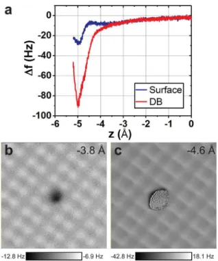
Figure 4a shows force curves acquired using a
H-function-alized tip above a surface hydrogen atom (blue curve) and a single silicon DB (red curve). These force curves were recorded subsequently with Z = 0 Å, corresponding to the tip position defined by the STM imaging set points (30 pA and +1.3 V) before switching off the feedback loop. Hence, superposing the two curves allows direct comparison of the interaction force between tip−surface and tip−DB. We notice that for relatively large tip−sample distances the two curves are almost identical. Only for small tip elevations (around −3.5 Å in this example) is a difference seen, with the DB showing a much larger increase in attractive interaction with the tip. This indicates that short-range forces are the main contributor to the interaction force.37
This is also consistent with the DB being a reactive chemical center on the chemically inert H−Si surface where deposited molecules can selectively adsorb.38,39 Similar to what was reported previously for the case of gold atoms adsorbed on NaCl over Cu(111),40,41the short-range electrostatic force due to the localized negative charge on the DB11,13,14is most likely the main contributor to the large tip−sample interaction on the DB.
Figure 4b and c show frequency shift maps acquired at
different tip elevations using a H-functionalized tip. At relatively large tip−sample distances (Figure 4b), each hydrogen atom decorating a silicon atom clearly appears and follows the dimer structure of the 2×1 reconstruction. The DB arising from the desorbed hydrogen atom on the surface appears as a dark atom-sized protrusion, introducing a much higher tip−sample interaction force localized on the DB. As we get closer to the surface (Supporting Information, Figure S2), an evolution from atomic to bond contrast is seen on the H−Si surface, as discussed in detail in ref 30. In Figure 4c, as a result of the larger attractive forces, the DB appears as an enlarged feature. The perturbations seen inside are an artifact in the excitation channel (Supporting Information, Figure S3), reflecting the inability of the feedback loop to maintain a constant oscillation amplitude due to quick changes in the interaction profile during lateral movement of the tip from the passivated region to the reactive DB feature. We comment that the instability is not visible in Δf(z) curves, as shown in Figure 4a, due to the absence of such quick changes.
We note here that high-resolution bond contrast imaging is rendered possible due to the passivation of the tip apex with a hydrogen atom.25,30 The later can be attracted to form a covalent bond with the silicon DB, but only at very small tip− sample elevations. This shows that the H-functionalized tip is robust and can be used to image reactive adsorbates or surface defects.
Altering Engineered on-Surface DB-Based Quantum Structures.Recent works have shown that a DB can behave as a single-atom quantum dot. Additionally, using atom-by-atom lithography with the STM tip, the coupling between DBs can be exploited to create functional DB structures such as QCA
Figure 4. NC-AFM characterization of a single DB on the H− Si(100)-2×1 surface using a H-functionalized tip. (a) Δf(z) curves recorded on the H−Si surface (blue curve) and on the silicon DB (red curve). 3 × 3 nm2frequency shift maps of a DB on the H−Si
surface at relatively large (b) and small (c) tip−sample distances, respectively. All data were acquired at 0 V with an oscillation amplitude of 1 Å.
ACS Nano Article
DOI:10.1021/acsnano.7b04238
ACS Nano2017, 11, 8636−8642
circuits, binary wires, and logic gates.11,12,17,42For large many-atom circuits this necessitates a precise control of desorption, which is difficult to achieve and has not been reported for more than a few DBs so far. Hence, a technique to correct or change multi-DB structures is highly desirable. Additionally, capping DBs would allow modulating the engineered quantum states from coupled DBs.16
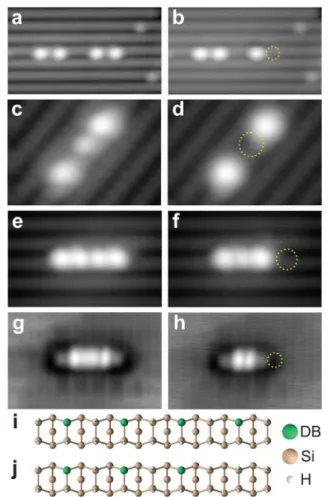
Figure 5a shows a filled-state STM image of two separate
pairs of coupled DBs along the same dimer row. Each pair has
two hydrogen atoms separating the DBs within the pair (see
Figure S4). We note here the enhanced STM contrast
characteristic of a H-functionalized tip. In Figure 5b, the right-side DB was selectively capped using the mechanically induced H−Si covalent bonding described in the previous section. We notice inFigure 5b the change in the STM contrast as previously shown inFigures 1and3. Additionally, the new single DB on the right side of the image appears as a bright
protrusion surrounded with a small dark halo, while the appearance of the two other coupled DBs shows no change.11
A similar experiment is shown in Figure 5c, where three tunnel-coupled DBs are imaged using a H-functionalized tip. The central DB was then erased, the tip was refunctionalized by picking up another hydrogen atom, and the remaining two DBs were reimaged inFigure 5d. Using an equivalent hydrogen tip for the before and after images highlights that changes in brightness are the result of coupling alterations, not simply a change of the terminating atom.
Figure 5e shows a filled-state image of four DBs along the
same dimer row with each DB separated by a single H atom, as illustrated in the 3D model ofFigure 5f. In the corresponding empty-state image (Figure 5g), a more complex structure is seen with four additional bright protrusions between the visible end atoms. Theoretical analyses from Schofield et al.16 have
reported similar results, explaining the extra protrusions as an excited-state molecular orbital from wave function overlap of multi-DB systems. We show here an active modification of these artificial molecular orbitals through the controlled mechanical covalent bonding of a Si atom (DB) with a hydrogen atom on the tip apex causing nodes to disappear.
Figure 5f and h respectively show the altered filled- and
empty-state molecular orbitals from erasing the far-right DB inFigure 5e. The filled-state image shows up as three bright protrusions corresponding to three DBs, whereas the empty-state image has been altered to now have only two bright protrusions instead of the prior four. We note that in the example ofFigure 5e to h DB structures were imaged using a nonfunctionalized tip both before and after alteration. This further highlights that changes in the coupling between DBs visible from the different additional nodes that appear/disappear are not due to changes in the tip, but rather the result of erasing a DB with a hydrogen on the tip apex.
Through the examples of Figure 5, we can see how the controlled mechanically induced H and Si covalent bonding allows the nondestructive editing of a DB structure. This technique could be further applied to actuation of more complicated DB-based patterns and elements as well, with erasure of a DB acting as a type of switch.
CONCLUSION
To summarize, we showed that following a tip-induced desorption, a hydrogen atom can be deposited on the surface or transferred to the tip apex, resulting in a H-functionalized tip. The physisorbed single hydrogen atom on the chemically inert H−Si surface could be stably imaged in STM and AFM modes. The H-functionalized tip was used to (i) characterize silicon dangling bonds and (ii) mechanically induce the covalent bonding of single hydrogen and silicon atoms. We showed the potential of this mechanically induced reaction to precisely modify multiple DB structures such as coupled DBs and artificial molecular states.
METHODS
Experiments were carried out using a commercial (Omicron) LT-STM/AFM system operated at 4.5 K. We used qPlus sensors exhibiting a quality factor Q ≃ 30 000 and a resonance frequency f0≃
25 kHz. Tips were direct current etched in a NaOH solution from a 50 μm thick polycrystalline tungsten wire. In ultrahigh vacuum (UHV), tips were first cleaned from their oxide layer by a series of electron beam heating treatments, followed by field evaporation in a field ion microscope (FIM). Then, they were further sharpened using a FIM Figure 5. Altering coupling and artificial molecular orbitals in
multi-DB structures. (a) Two pairs of coupled DBs on the H− Si(100) surface arranged along the same dimer row. (b) Image of the same area after the mechanically induced capping of the far-right DB in (a). (c) A 3 × 2 nm2 STM image of three
tunnel-coupled DBs. (d) The same area after erasing the middle DB in (c). Constant current images (a) to (d) were acquired at −1.8 V and 50 pA. (e, f) Filled (−2.0 V, 50 pA) and (g, h) empty (+1.4 V, 50 pA) states STM images of a DB wire, respectively, before and after erasing the far-right DB in (e). 3D models of the four (i) and three (j) DB wires. Positions of erased DBs are indicated by dotted circles. Empty-state images of (a) and (c) are presented in Supplementary Figure S4.
nitrogen etching process to ensure a small tip radius of curvature.43 The sensor was equipped with a separate wire for tunneling current to minimize cross-talk problems.44 Additionally, all AFM data were recorded at 0 V to avoid coupling between frequency shift and tunnel current, as well as imaging artifacts such as phantom force.45,46
In situ, tips were further processed to obtain artifact-free images by
first creating a bare silicon patch through tip-induced hydrogen desorption, then by controlled nanoindentation on the created patch. This procedure usually results in a clean and stable tip. From prior work, this treatment was shown to result in a silicon tip.30,47
We used highly arsenic-doped (∼1.5 × 10¹⁹ atom cm−3) silicon
(100) samples. Following 12 h of degassing at ∼600 °C in UHV, samples underwent a series of resistive flash anneals at 1250 °C. Samples were then exposed to atomic hydrogen while being kept at ∼320 °C to ensure a 2×1 reconstruction.
To minimize drift during AFM image acquisition, the tip was left to settle for about 12 h after approach to allow piezo scanner stabilization. Additionally, an atom tracking program implemented in the Nanonis control electronics was used.
ASSOCIATED CONTENT
*
S Supporting InformationThe Supporting Information is available free of charge on the
ACS Publications websiteat DOI:10.1021/acsnano.7b04238.
(i) STM images showing a physisorbed hydrogen being laterally manipulated with STM to cap a DB; (ii) images of an isolated DB and the background hydrogen-terminated surface in different height-modulated inter-action regimes; (iii) simultaneously acquired frequency shift and excitation measurements showing the DB as a reactive center; (iv) empty-state STM images forFigure 5a and c (PDF) AUTHOR INFORMATION Corresponding Authors *E-mail: taleana@ualberta. *E-mail: rwolkow@ualberta.ca. ORCID Taleana R. Huff:0000-0002-6876-8265 Author Contributions
⊥T. R. Huff and H. Labidi contributed equally to this work.
Notes
The authors declare the following competing financial interest(s): A patent has been filed on this subject with Taleana Huff, Moe Rashidi, and Robert Wolkow as inventors. R. Wolkow is the Chief Technical Officer of Quantum Silicon Inc (QSi). QSi is seeking to commercialize atomic silicon quantum dot based technologies.
ACKNOWLEDGMENTS
We thank M. Cloutier for his technical expertise and J. Pitters for valuable discussions. We also thank NRC, NSERC, QSi, and AITF for financial support.
REFERENCES
(1) Beyer, M. K.; Clausen-Schaumann, H. Mechanochemistry: The Mechanical Activation of Covalent Bonds. Chem. Rev. (Washington,
DC, U. S.) 2005, 105, 2921−2948.
(2) Custance, O.; Perez, R.; Morita, S. Atomic Force Microscopy as a Tool for Atom Manipulation. Nat. Nanotechnol. 2009, 4, 803−810.
(3) Sweetman, A.; Jarvis, S.; Danza, R.; Bamidele, J.; Gangopadhyay, S.; Shaw, G. A.; Kantorovich, L.; Moriarty, P. Toggling Bistable Atoms
via Mechanical Switching of Bond Angle. Phys. Rev. Lett. 2011, 106,
136101.
(4) Ternes, M.; Lutz, C. P.; Hirjibehedin, C. F.; Giessibl, F. J.; Heinrich, A. J. The Force Needed to Move an Atom on a Surface.
Science 2008, 319, 1066−1069.
(5) Langewisch, G.; Falter, J.; Fuchs, H.; Schirmeisen, A. Forces During the Controlled Displacement of Organic Molecules. Phys. Rev.
Lett. 2013, 110, 036101.
(6) Jarvis, S. P.; Taylor, S.; Baran, J. D.; Champness, N. R.; Larsson, J. A.; Moriarty, P. Measuring the Mechanical Properties of Molecular Conformers. Nat. Commun. 2015, 6, 8338.
(7) Ladenthin, J. N.; Frederiksen, T.; Persson, M.; Sharp, J. C.; Gawinkowski, S.; Waluk, J.; Kumagai, T. Force-Induced Tautomeriza-tion in a Single Molecule. Nat. Chem. 2016, 8, 935−940.
(8) Dujardin, G.; Mayne, A.; Robert, O.; Rose, F.; Joachim, C.; Tang, H. Vertical Manipulation of Individual Atoms by a Direct STM Tip-Surface Contact on Ge(111). Phys. Rev. Lett. 1998, 80, 3085−3088.
(9) Oyabu, N.; Custance, Ó.; Yi, I.; Sugawara, Y.; Morita, S. Mechanical Vertical Manipulation of Selected Single Atoms by Soft Nanoindentation Using Near Contact Atomic Force Microscopy. Phys.
Rev. Lett. 2003, 90, 176102.
(10) Sugimoto, Y.; Abe, M.; Hirayama, S.; Oyabu, N.; Custance, Ó.; Morita, S. Atom Inlays Performed at Room Temperature Using Atomic Force Microscopy. Nat. Mater. 2005, 4, 156−159.
(11) Haider, M. B.; Pitters, J. L.; DiLabio, G. A.; Livadaru, L.; Mutus, J. Y.; Wolkow, R. A. Controlled Coupling and Occupation of Silicon Atomic Quantum Dots at Room Temperature. Phys. Rev. Lett. 2009,
102, 046805.
(12) Wolkow, R. A.; Livadaru, L.; Pitters, J.; Taucer, M.; Piva, P.; Salomons, M.; Cloutier, M.; Martins, B. V. Field-Coupled
Nano-computing; Springer, 2014; pp 33−58.
(13) Taucer, M.; Livadaru, L.; Piva, P. G.; Achal, R.; Labidi, H.; Pitters, J. L.; Wolkow, R. A. Single-Electron Dynamics of an Atomic Silicon Quantum Dot on the H-Si(100) - (2 × 1) Surface. Phys. Rev.
Lett. 2014, 112, 256801.
(14) Labidi, H.; Taucer, M.; Rashidi, M.; Koleini, M.; Livadaru, L.; Pitters, J.; Cloutier, M.; Salomons, M.; Wolkow, R. A. Scanning Tunneling Spectroscopy Reveals a Silicon Dangling Bond Charge State Transition. New J. Phys. 2015, 17, 073023.
(15) Livadaru, L.; Xue, P.; Shaterzadeh-Yazdi, Z.; DiLabio, G. A.; Mutus, J.; Pitters, J. L.; Sanders, B. C.; Wolkow, R. A. Dangling-Bond Charge Qubit on a Silicon Surface. New J. Phys. 2010, 12, 083018.
(16) Schofield, S. R.; Studer, P.; Hirjibehedin, C. F.; Curson, N. J.; Aeppli, G.; Bowler, D. R. Quantum Engineering at the Silicon Surface Using Dangling Bonds. Nat. Commun. 2013, 4, 1649.
(17) Kolmer, M.; Zuzak, R.; Dridi, G.; Godlewski, S.; Joachim, C.; Szymonski, M. Realization of a Quantum Hamiltonian Boolean Logic Gate on the Si(001):H Surface. Nanoscale 2015, 7, 12325−12330.
(18) Shen, T.-C.; Wang, C.; Abeln, G. C.; Tucker, J. R.; Lyding, J. W.; Avouris, P.; Walkup, R. E. Atomic-Scale Desorption Through Electronic and Vibrational Excitation Mechanisms. Science 1995, 268, 1590−1592.
(19) Foley, E. T.; Kam, A. F.; Lyding, J. W.; Avouris, P. Cryogenic UHV-STM Study of Hydrogen and Deuterium Desorption from Si(100). Phys. Rev. Lett. 1998, 80, 1336−1339.
(20) Soukiassian, L.; Mayne, A. J.; Carbone, M.; Dujardin, G. Atomic-Scale Desorption of H Atoms From the Si(100) - 2 × 1:H Surface: Inelastic Electron Interactions. Phys. Rev. B: Condens. Matter Mater.
Phys. 2003, 68, 035303.
(21) Walsh, M. A.; Hersam, M. C. Atomic-Scale Templates Patterned by Ultrahigh Vacuum Scanning Tunneling Microscopy on Silicon.
Annu. Rev. Phys. Chem. 2009, 60, 193−216.
(22) Schmucker, S.; Kumar, N.; Abelson, J.; Daly, S.; Girolami, G.; Bischof, M.; Jaeger, D.; Reidy, R.; Gorman, B.; Alexander, J.; Ballard, J.; Randall, J.; Lyding, J. Field-Directed Sputter Sharpening for Tailored Probe Materials and Atomic-Scale Lithography. Nat.
Commun. 2012, 3, 935.
(23) Møller, M.; Jarvis, S. P.; Guérinet, L.; Sharp, P.; Woolley, R.; Rahe, P.; Moriarty, P. Automated Extraction of Single H Atoms with STM: Tip State Dependency. Nanotechnology 2017, 28, 075302.
ACS Nano Article
DOI:10.1021/acsnano.7b04238
ACS Nano2017, 11, 8636−8642
(24) Pavliček, N.; Majzik, Z.; Meyer, G.; Gross, L. Passivation of Dangling Bonds on Hydrogenated Si(100)-2 × 1: A Possible Method for Error Correction in Hydrogen Lithography. arXiv.org, e-Print Arch.,
Condens. Matter 2017. arXiv:1706.02560v2. 1−5.
(25) Gross, L.; Mohn, F.; Moll, N.; Liljeroth, P.; Meyer, G. The Chemical Structure of a Molecule Resolved by Atomic Force Microscopy. Science 2009, 325, 1110−1114.
(26) Sharp, P.; Jarvis, S.; Woolley, R.; Sweetman, A.; Kantorovich, L.; Pakes, C.; Moriarty, P. Identifying Passivated Dynamic Force Microscopy Tips on H:Si(100). Appl. Phys. Lett. 2012, 100, 233120.
(27) Lantz, M. A.; Hug, H. J.; Hoffmann, R.; van Schendel, P. J. A.; Kappenberger, P.; Martin, S.; Baratoff, A.; Güntherodt, H.-J. Quantitative Measurement of Short-Range Chemical Bonding Forces.
Science 2001, 291, 2580−2583.
(28) Sugimoto, Y.; Pou, P.; Abe, M.; Jelinek, P.; Pérez, R.; Morita, S.; Custance, Ó. Chemical Identification of Individual Surface Atoms by Atomic Force Microscopy. Nature 2007, 446, 64−67.
(29) Mohn, F.; Gross, L.; Meyer, G. Measuring the Short-Range Force Field Above a Single Molecule with Atomic Resolution. Appl.
Phys. Lett. 2011, 99, 053106.
(30) Labidi, H.; Koleini, M.; Huff, T.; Salomons, M.; Cloutier, M.; Pitters, J.; Wolkow, R. A. Indications of Chemical Bond Contrast in AFM Images of a Hydrogen-Terminated Silicon Surface. Nat.
Commun. 2017, 8, 14222.
(31) Ballard, J. B.; Owen, J. H. G.; Alexander, J. D.; Owen, W. R.; Fuchs, E.; Randall, J. N.; Longo, R. C.; Cho, K. Spurious Dangling Bond Formation During Atomically Precise Hydrogen Depassivation Lithography on Si(100): The Role of Liberated Hydrogen. J. Vac. Sci.
Technol., B: Nanotechnol. Microelectron.: Mater., Process., Meas., Phenom.
2014, 32, 021805.
(32) Bartels, L.; Meyer, G.; Rieder, K.-H.; Velic, D.; Knoesel, E.; Hotzel, A.; Wolf, M.; Ertl, G. Dynamics of Electron-Induced Manipulation of Individual CO Molecules on Cu(111). Phys. Rev.
Lett. 1998, 80, 2004−2007.
(33) Mohn, F.; Schuler, B.; Gross, L.; Meyer, G. Different Tips for High-Resolution Atomic Force Microscopy and Scanning Tunneling Microscopy of Single Molecules. Appl. Phys. Lett. 2013, 102, 073109. (34) Yurtsever, A.; Sugimoto, Y.; Tanaka, H.; Abe, M.; Morita, S.; Ondráček, M.; Pou, P.; Pérez, R.; Jelínek, P. Force Mapping on a Partially H-Covered Si(111)-(7 × 7) Surface: Influence of Tip and Surface Reactivity. Phys. Rev. B: Condens. Matter Mater. Phys. 2013, 87, 155403.
(35) Sugimoto, Y.; Pou, P.; Custance, O.; Jelinek, P.; Abe, M.; Perez, R.; Morita, S. Complex Patterning by Vertical Interchange Atom Manipulation Using Atomic Force Microscopy. Science 2008, 322, 413−417.
(36) Berger, J.; Spadafora, E. J.; Mutombo, P.; Jelínek, P.; Švec, M. Force-Driven Single-Atom Manipulation on a Low-Reactive Si Surface for Tip Sharpening. Small 2015, 11, 3686−3693.
(37) Such, B.; Kolmer, M.; Godlewski, S.; Lis, J.; Budzioch, J.; Wojtaszek, M.; Szymonski, M. In Imaging and Manipulation of
Adsorbates Using Dynamic Force Microscopy; Moriarty, P., Gauthier,
S., Eds.; Advances in Atom and Single Molecule Machines; Springer International Publishing, 2015; pp 111−118.
(38) Piva, P. G.; DiLabio, G. A.; Pitters, J. L.; Zikovsky, J.; Rezeq, M.; Dogel, S.; Hofer, W. A.; Wolkow, R. A. Field Regulation of Single-Molecule Conductivity by a Charged Surface Atom. Nature 2005, 435, 658−661.
(39) Godlewski, S.; Kolmer, M.; Kawai, H.; Such, B.; Zuzak, R.; Saeys, M.; de Mendoza, P.; Echavarren, A. M.; Joachim, C.; Szymonski, M. Contacting a Conjugated Molecule with a Surface Dangling Bond Dimer on a Hydrogenated Ge(001) Surface Allows Imaging of the Hidden Ground Electronic State. ACS Nano 2013, 7, 10105−10111.
(40) Gross, L.; Mohn, F.; Liljeroth, P.; Repp, J.; Giessibl, F. J.; Meyer, G. Measuring the Charge State of an Adatom with Noncontact Atomic Force Microscopy. Science 2009, 324, 1428−1431.
(41) Bocquet, F.; Nony, L.; Loppacher, C. Polarization Effects in Noncontact Atomic Force Microscopy: A Key to Model the
Tip-Sample Interaction Above Charged Adatoms. Phys. Rev. B: Condens.
Matter Mater. Phys. 2011, 83, 035411.
(42) Hitosugi, T.; Heike, S.; Onogi, T.; Hashizume, T.; Watanabe, S.; Li, Z.-Q.; Ohno, K.; Kawazoe, Y.; Hasegawa, T.; Kitazawa, K. Jahn-Teller Distortion in Dangling-Bond Linear Chains Fabricated on a Hydrogen-Terminated Si(100)- 2 × 1 Surface. Phys. Rev. Lett. 1999,
82, 4034−4037.
(43) Labidi, H.; Kupsta, M.; Huff, T.; Salomons, M.; Vick, D.; Taucer, M.; Pitters, J.; Wolkow, R. A. New Fabrication Technique for Highly Sensitive qPlus Sensor with Well-Defined Spring Constant.
Ultramicroscopy 2015, 158, 33−37.
(44) Majzik, Z.; Setvín, M.; Bettac, A.; Feltz, A.; Cháb, V.; Jelínek, P. Simultaneous Current, Force and Dissipation Measurements on the Si(111) 7 × 7 Surface with an Optimized qPlus AFM/STM Technique. Beilstein J. Nanotechnol. 2012, 3, 249−259.
(45) Nony, L.; Bocquet, F.; Para, F.; Loppacher, C. Frequency Shift, Damping, and Tunneling Current Coupling with Quartz Tuning Forks in Noncontact Atomic Force Microscopy. Phys. Rev. B: Condens.
Matter Mater. Phys. 2016, 94, 115421.
(46) Weymouth, A. J.; Wutscher, T.; Welker, J.; Hofmann, T.; Giessibl, F. J. Phantom Force Induced by Tunneling Current: A Characterization on Si(111). Phys. Rev. Lett. 2011, 106, 226801.
(47) Jarvis, S.; Sweetman, A.; Bamidele, J.; Kantorovich, L.; Moriarty, P. Role of Orbital Overlap in Atomic Manipulation. Phys. Rev. B: