HAL Id: hal-03224109
https://hal.archives-ouvertes.fr/hal-03224109
Submitted on 11 May 2021HAL is a multi-disciplinary open access archive for the deposit and dissemination of sci-entific research documents, whether they are pub-lished or not. The documents may come from teaching and research institutions in France or abroad, or from public or private research centers.
L’archive ouverte pluridisciplinaire HAL, est destinée au dépôt et à la diffusion de documents scientifiques de niveau recherche, publiés ou non, émanant des établissements d’enseignement et de recherche français ou étrangers, des laboratoires publics ou privés.
The Effect of X-Ray Irradiation on Conductivity of C
and 2 C Polytype TlInS 2 Ferroelectrics
Mykola Borovyi, Yurii Gololobov, Karyna Isaieva, Mykola Isaiev
To cite this version:
Mykola Borovyi, Yurii Gololobov, Karyna Isaieva, Mykola Isaiev. The Effect of X-Ray Irradiation on Conductivity of C and 2 C Polytype TlInS 2 Ferroelectrics. physica status solidi (b), Wiley, 2021, 258 (5), pp.2000556. �10.1002/pssb.202000556�. �hal-03224109�
1
The effect of X-ray irradiation on conductivity of C and 2C polytypes TlInS
2ferroelectrics
M.O. Borovyi*, Yu.P. Gololobov, K. Isaievaand M. Isaiev
*Prof. M.O. Borovyi
Faculty of Physics, Taras Shevchenko National University of Kyiv, 64/13, Volodymyrska Str., Kiev 01601, Ukraine; mborovyi1@gmail.com
Prof. Yu.P. Gololobov
Department of Physics, National Transport University, Suvorova Street 1, 01010 Kyiv, Ukraine Dr. K. Isaieva
Université de Lorraine, INSERM, IADI, Nancy, F-54000, France Dr. M. Isaiev
Université de Lorraine, CNRS, LEMTA (UMR 7563), Nancy, F-54000, France
Keywords: electrical conductivity, ferroelectrics, commensurate, incommensurate phases
The influence of X-ray irradiation on DC conductivity of TlInS2 C and 2C polytypes are studied in temperature range of 100 – 300 K. The X-ray irradiation (absorbed doses are 0.9 kGy and 2.7 kGy) leads to an increasing conductivity of both C- and 2C-samples in proportion to the absorbed dose; the conductivity decreases on cooling in temperature region of 100 – 300 K. An anomaly increase of conductivity is observed in C-polytype samples on cooling in temperature range of the incommensurate phase existence (197 – 214 K). The X-ray irradiation causes the "blur" of that anomaly. It is established that the mechanism of hopping conductivity with variable hopping length takes place for both polytypes in temperature range of 125 – 175 K and the densities of localized states near the Fermi level (NF) are determined. Under irradiation the density NF increases from 3.71018 eV-1cm-3 (C) and 6.91018 eV-1cm-3 (2C) and exceeds the initial more than three times at D = 2.7 kGy. Using the one-dimensional Kroning-Penney model, the role of incommensurate periodic potential in modification of electron band structure at creation the incommensurate phases in crystals is discussed.
2
1. Introduction
-TlInS2 crystals are the wide-gap semiconductor-ferroelectrics and belong to the class of low-dimensional thallium compounds TlMX2 (M = Ga, In; X = Se, S, Te). At ambient conditions -TlInS2 crystals are characterized by C2/c space symmetry group of the monoclinic crystal system; unit cell parameters are а = 10.90 Å, b = 10.94 Å, с = 15.18 Å, = 100.21.[1] Since TlInS2 crystals are promising materials as detectors of electromagnetic radiation, their dielectric, optical, elastic properties, electric transport has been actively studied in numerous works.[2 – 5] It was found a number of anomalies of photoconductivity, permittivity, ultrasonic wave propagation velocity and specific heat of TlInS2 crystals which are due to the existence of phase transitions (PT) in them with the formation of both commensurate and incommensurate modulated structures in temperature range of 170 – 240 K (as also in isostructural analog TlGaSe2 but in temperature range 100 – 160 K).[2,6,7] However, despite numerous experimental studies, data on the characteristics and mechanisms of PT "paraelectric – incommensurate phase (IP)" and "IP - commensurate phase (CP)" in TlInS2 are quite contradictory. For example, according to neutron diffraction data,[8] modulation satellites in corresponding to IP are observed in temperature range of T = 200 – 216 K with a modulation vector q( , , 0.25) ( =0.012). From another side, the X-ray diffraction data in temperature range of T = 194 – 214 K indicate the formation of incommensurate waves with the wavevector q( ,0, 0.25) ( =0.04) as the waves of static atomic displacements.[1,9] It was suggested that the incommensurate atomic displacements occur in the a-direction of monoclinic unit cell so the wavelength of incommensurability is the irrational number = =a 1/ 22.72.... According to that model atoms with the same value of Z-coordinate are displaced in the a–b-plane by the same amount, and the Z-component of displacement is characterized by =c 4c.
To explain the discrepancy between neutron and X-ray diffraction data, as well as number of other contradictions, it was suggested take into account the existence of a number of polytypes in the -TlInS2 crystals - C, 2C, 4C and 8C with the unit cell parameter c = c ', 2c', 4c ', 8c' (c'
15
Å), respectively.[10,11] In particular, for TlInS2 crystals of 2C polytype the absence of modulation satellites of IP and CP in temperature range of 170 – 300 K, which points to absence of incommensurate and commensurate modulation waves, unlike the C polytype, was demonstrated with four circle X-ray diffractometry method.[9,12] Because of these differences of the C and 2C polytypes crystal lattice dynamics, it is crucial compare the transport characteristics of these polytypes, in particular, their electrical conductivity. Since the conductivity of TlInS2 is
3
very sensitive to changes of the defect’s concentration level,[13–15] it is important to study the electrical conductivity of TlInS2 C and 2C polytypes at various doses of X-ray irradiation in temperature range of 100 – 300 K. The paper presents the results of such research.
2. Experimental procedure
The single-crystal samples of TlInS2 C and 2C polytypes grown by the Bridgman– Stockbarger method were used for electrical conductivity measurements. The elemental composition and stoichiometry of the samples were verified by a local elemental analysis technique using energy-dispersive X-ray spectroscopy EDX (the JEOL JEM-2100F TEM). The X-ray diffraction identification of C and 2C polytypes were performed by using a diffractometer DRON-4-07 with a single-crystal goniometer head GP-15. The typical size of rectangular samples was (5x7x0.1) mm; the surfaces (5x7) mm coincided with the cleavage planes (001). Silver probes were applied on both two surfaces (7x0.1) mm using Vacuum spraying method. At that electrodes arrangement the conductivity was measured along a cleavage plane. The samples were placed in the cryostat chamber CS204AEX1-AL; the temperature of samples was controlled using the Lake Shore 331S controller. The range of measurements were performed in the cooling mode (in some cases - in heating mode too) with temperature step 2 K, the rate of temperature change was 1 K / min, the accuracy of maintaining the temperature was 0.1 K.
A DC voltage which was formed by a 12-bit analog-to-digital converter and a buffer amplifier was applied to the sample. The voltage variation on the sample was = − − +U ( 5) ( 5) V. The current in the sample was converted to voltage using a current-voltage converter, and it was controlled using a 16-bit analog-to-digital converter. The measuring range of current (I) was depended on the resistance of the current-voltage converter (for example, for resistance 30 MΩ the maximum current was about 35 nA), and the minimal current value was determined by the input current of the converter (2 pA in our case). The current – voltage characteristic of the sample was measured at each temperature in the voltage rangeU, on which the linear regions were distinguished in the low-voltage region Ul −( 0.04) ( 0.04)− + V. The conductivity was calculated as =
(
U I/)
−1( / )l S (l - length, S - surface area of sample) at two identical voltage values, but different in polarity; for further analysis the averaged conductivity value was used.The irradiation of samples was performed by the radiation of the X-ray tube BHV-12 Pd (voltage 30 kV, current 50 mA). The spectrum of X-ray radiation includes the characteristic K and K lines (photons energies were 21.2 keV and 23.8 keV, respectively), L - series lines (2.7– 2.9 keV) and bremsstrahlung. The sample was placed parallel to the plane of the X-Ray tube
4
beryllium window at the distance of 7 cm. The radiation was directed perpendicular to the cleavage surface (5x7) mm and was absorbed in a layer of 0.1 mm thick. To achieve a uniform irradiation in volume, the samples were irradiated from two sides. The PTW 23342 soft X-ray ionization chamber has been used to measure the absorbed X-ray dose rate. The dose rate was 1.25 mGy/min when chamber was installed in place of the sample. Each sample was initially irradiated for 12 h (6h for each side) and subsequently for another 24 h (12h for each side) so that the absorbed doses were 0.9 and 2.7 KGy, respectively.
3. Experimental Results
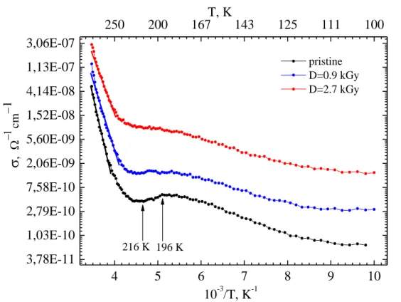
Figure 1 shows typical temperature dependences ( )T for samples of C-polytype TlInS2 crystals both pristine and irradiated. For the unirradiated C-samples under cooling in temperature range of 255 – 290 K an exponential dependence ( )T with the activation energy of the charge carriers Ea = 0.650.04 eV is observed.
Figure 1. The dependence
(T
)
for C-samples TlInS2. The activation energies: Ea = 0.650.04
eV (pristine), Ea = 0.530.04 eV (0.9 kGy), Ea = 0.440.04eV ( 2.7 kGy)
At T < 250 K the deviation of ( )T from exponential was increasingly prominent, so the curve is flat at temperatures 214 - 217 K. Surprisingly, the further cooling is accompanied by an increase of conductivity, but already at 195 – 200 K the dependence ( )T reaches the maximum of the increase. Finally, at the T < 195 K the electrical conductivity monotonically decreases. Thus,
4 5 6 7 8 9 10 250 200 167 143 125 111 100 3,78E-11 1,03E-10 2,79E-10 7,58E-10 2,06E-09 5,60E-09 1,52E-08 4,14E-08 1,13E-07 3,06E-07
− cm − 1 10-3/T, K-1 pristine D=0.9 kGy D=2.7 kGy 216 K 196 K T, K5
on cooling in the range of 195 – 214 K, in which the IP order parameter linearly increases,[1] the dependence ( )T exhibits temperature behaviour anomalous for semiconductors. In contrast, upon subsequent heating of the samples, cooled to 100 K, in the temperature range of 195 K → 214 К the conductivity was rising monotonically. Figure 1 also presents the ( )T
dependences on cooling for irradiated C-samples under two X-ray absorbed doses. First, there an increasing trend in the conductivity with absorbed dose growing was observed. It should be noted that as the absorbed dose increases, the anomaly on ( )T dependence on cooling in the range of 195 - 214 K is "blurred", so for the dose D = 2.7 kGy the increase of the conductivity in that temperature range is practically not observed. For irradiated samples, at T = 245 K – 300 K on the
( )T
, there are also exponential regions. As the absorbed doses increases, the activation energy decreases: Ea = 0.530.04 eV for D = 0.9 kGy and Ea = 0.440.04eV for D = 2.7 kGy.
In Figure 2 the ( )T dependences are shown for samples of 2C-polytype TlInS2 crystals. For 2C-samples ( )T dependences are substantially different: in the entire temperature range on cooling the conductivity decreases monotonically including the range of 195 – 217 К.
Figure 2. The dependence
(T
)
for 2C-samples TlInS2. The activation energies: a) T = 200 – 255 K Ea (1) = 0.510.04 eV (pristine), Ea (1) = 0.400.04eV (0.9 kGy); Ea (2) = 0.310.04 eV (2.7 kGy); b) T = 255 – 300 K Ea (2) = 0.200.04 eV (pristine), Ea (2) = 0.130.04eV (0.9 kGy), Ea (2) = 0.120.04 eV (2.7 kGy) 4 5 6 7 8 9 10 250 200 167 143 125 111 100 1.03E-10 2.79E-10 7.58E-10 2.06E-09 5.60E-09 1.52E-08 4.14E-08 1.13E-07 3.06E-07 8.32E-07 pristine D=0.9 kGy D=2.7 kGy − cm − 1 10−3/T, K−1 T, K6
Two temperature regions with the various exponential dependences (T) are distinguished in temperature range 200 – 300 K for both unirradiated and irradiated samples: the range 255 - 300 K (1) with Ea (1) = 0.510.04 eV (unirradiated), Ea (1) = 0.400.04eV (0.9 kGy) and Ea (1) = 0.31
0.04
eV (2.7 kGy), and the range 200 – 255 K (2) with Ea (2) = 0.200.04 eV (unirradiated),
Ea (2) = 0.130.04eV (0.9 kGy) and Ea (2) = 0.120.04 eV (2.7 kGy). The dependences ( )T
on cooling and subsequent heating in contrast to C-samples are rather close and in range of 250 – 300 K are exponential with Ea = 0.510.04 eV and Ea = 0.470.04 eV, respectively. The
absence of features on the ( ) T dependence for 2C-samples in temperature range of 197 – 214 K, in which the IP exists in the C-polytype crystals, agrees well with the X-ray diffraction data regarding the absence of modulated structures in the TlInS2 crystals of 2C polytype.[8,11] As well as C-polytype, there is an electrical conductivity growing with increasing absorbed dose, and exponential dependences of ( ) T at T = 255 K – 300 K with Ea = 0.510.04 eV (unirradiated),
Ea = 0.400.04eV (0.9 kGy) and Ea = 0.310.04 eV (2.7 kGy) are registries.
In summary, the main experimental results state: i) an anomaly behavior of conductivity in C-polytype samples at cooling in the temperature range of the IP existence (195 – 214 K), the X-ray irradiation causes the "blur" of that anomaly; ii) the conductivity of 2C-samples at cooling over the temperature range of 100 –300 K is monotonically decreasing; iii) the X-ray irradiation leads to an increasing conductivity of both C- and 2C-samples.
4. Discussion
4.1. The conductivity parameters of the TlInS2 crystals
It was previously found that high defective crystals TlInS2 with layered structure are characterized by a high concentration of localized states ( 1018 eV-1
cm-3) in the bandgap near the Fermi level, and electron hopping conductivity along localized states is realized in them.[13,16] The exponential regions of the dependences ( )T for C-samples at 255 – 300 K and too exponential regions for 2C-samples at 200 – 255 K, 255 – 300 K correspond to conductivity with hopping activation energies of 0.1 – 0.7 eV. In such systems, upon further cooling one can expect the appearance of hopping conductivity with a variable hopping length. In that case, the temperature dependence of the conductivity takes the form = 0exp( BT− −1 4/ ) (Mott equation), where B=2a−3 4/(
kNF)
−1 4/ (a is radius of localization in electron wave function7
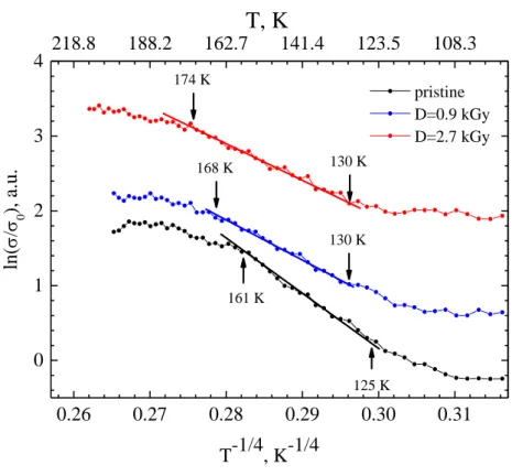
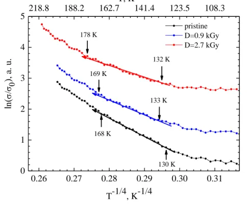
exp( r / a ) − , k is Boltzmann's constant, NF is the density of states near the Fermi level).[17] In order to clarify the existence of such conductivity the temperature dependence ( )T was analyzed in coordinates ln( / vs. 0) T−1 4/ . Figure 3 and Figure 4 are presented these dependences for radiated and irradiated samples of C- and 2C-polytypes on cooling in temperature range 100 – 205 K.
Figure 3. The dependences ln( / as function of 0) T−1 4/ for C-samples TlInS2
The approximating straight lines were constructed by the linear least squares method. As can be seen, for both C and 2C polytypes the linear dependences ln( / vs. 0) T−1 4/ are observed in some temperature intervals, which points to hopping conductivity with a variable hopping length there. Based on the slope of the straight lines, parameter B was determined and values of NF has been estimated. The localization radius of a = 1.4 nm was used.[16] The values of B and
F
N , as well as the experimentally measured values of conductivity at 300 K for all types of samples are given in the Table 1. For the unirradiated C-samples NF = 3 7 10. 18 eV-1 cm-3 was obtained, that
0.26 0.27 0.28 0.29 0.30 0.31 218.8 188.2 162.7 141.4 123.5 108.3 0 1 2 3 4 pristine D=0.9 kGy D=2.7 kGy ln ( / 0 ), a .u. T-1/4, K-1/4 161 K 125 K 168 K 130 K 130 K 174 K
T, K
8
agrees well with result of measured on AС.[12] After irradiation the concentration NF increases and at D = 2.7 kGy exceeds the initial more than three times. A similar result was obtained for
Figure 4. The dependences ln( / as function of 0) T−1 4/ for 2C-samples TlInS2
irradiated 2C-samples. It is important to note that the increase of NF is accompanied by an increase of the sample’s conductivity (see Table 1).
0.26 0.27 0.28 0.29 0.30 0.31 218.8 188.2 162.7 141.4 123.5 108.3 0 1 2 3 4 5 133 K 169 K pristine D=0.9 kGy D=2.7 kGy l n ( / ) , a. u. T-1/4, K-1/4 178 K 132 K 168 K 130 K T, K
Table 1. The conductivity parameters of the TlInS2 С and 2С polytypes
D, kGy C 2C σ (300 K), Ω-1 cm-1 unirradiated 5.110-8 8.210-8 0.9 1.310-7 1.610-7 2.7 2.910-7 7.810-7 B, K1/4 unirradiated 65±3 56±3 0.9 54±3 48±3 2.7 47±3 42±3 N(Ef), eV-1 cm-3 unirradiated 3.71018 6.91018 0.9 7.71018 1.31019 2.7 1.41019 2.11019
9
This testifies once again to the hopping conduction along localized states near the Fermi level in the TlInS2 crystals.
4.2. The generation of defects in the TlInS2 crystals under X-ray irradiation
Let us consider the possible channels of radiation defects generation in TlInS2 crystals by photons with a highest energy of 21 keV (Pd K , lines are the dominant components in spectrum of X-ray irradiation). The main mechanism of the of X-ray photons interaction with matter is atomic photoeffect if the photons energies below 100 keV[18]. This is especially true for soft X-rays with energy E(K) = 21 keV. The photoelectrons with kinetic energies Ee =E K( −) Ei are ejected from atoms as the result of ionization of the atomic electron shells (Ei - ionization potential
of i-shell). In the case of the TlInS2 crystals the range of the photoelectrons energies is 5 – 21 keV. At the next step, the photoelectrons undergo inelastic collisions with atoms, followed by secondary ionization of atoms. The energy transferred by a photoelectron to an atom of mass Ma can be estimated as Emax =4E m / ( Me e a+m )e 2,
m
e - mass of the electron.[19] For sulphur atom (the lightest atoms in the crystal TlInS2, Ma( )S 5.9 10 4me) it is Emax 1 4, eV, while in semiconductors with ionic-covalent bonds the energy of atom’s exit from lattice point is not less than 7 – 10 eV.[20]Therefore, at under-threshold irradiation the impact elastic-shifting mechanism of radiation defects creation in TlInS2 does not work. But in that case the major role in the generation of defects plays the impurity atoms charged. The concentration of defects in unirradiated TlInS2 crystals is high enough (1018cm–1), and significant part of them is caused by impurities that are incorporated into the crystal lattice at the stage of crystal growth.[19] Then, ionization of atom in the regular position of the crystal lattice (when the charged impurity atom is in certain vicinity of it) is accompanied by the Coulomb interaction of created ion with the impurity atom. As a result, an atom exits to the internode site and forms a vacancy with a fairly high probability.[20] As shown,[19] it is most probable for TlInS2 crystals the arrangement of impurity atoms in the centre of the InS4 octahedra at replacement of In atoms. Therefore, the ionization of sulphur atoms is accompanied by the appearance of anionic sulphur vacancies. In this case the creation of neutral complexes formed by anionic vacancies, charged impurity atoms and sulphur atoms in interstitials is possible. Unfortunately, we are not aware of papers in which the classification of defects in TlInS2 crystals have been performed and their quantitative parameters presented. However, above qualitative
10
consideration shows that in TlInS2 crystals at under-threshold irradiation there may be a rather effective impurity-ionization mechanism of intrinsic defect formation.
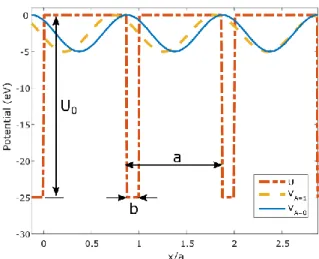
4.3. The one-dimensional model of the static modulation waves effect on the band structure
An interesting experimental result is an increasing of C-samples conductivity on cooling in temperature range of incommensurate phase existence 195 – 214 K. It should be noted that an increasing the TlInS2 conductivity on cooling was reported earlier,[16] however, the effect was observed in temperatures of 240 – 270 К, i.e. in the paraelectric rather than incommensurate phase. The fact the increase of conductivity on cooling C-samples begins at the appearance of IP (214 K) and finishes at the IP – CP PT (197 K) indicates that the presence of incommensurate displacement waves with the wave vector q( ,0,0.25)
( =0.04) effects noticeably on the electrons transport. That influence can be associated with the appearance in IP an additional potential with the wave vectorq( ,0,0.25)
, which superimposes on the periodic potential of the crystal lattice.Figure 5. The rectangular Kroning-Penney and periodic modulation potentials
For this assumption verification we consider the following simple model of band structure with static modulation waves in crystal lattice. The lattice was simulated with the one-dimensional rectangular Kroning-Penney potential U x( ) with the period equal to a, width of the well equal to b and the depth equal to U0. The presence of the incommensurate phase was simulated with the following potential: 0 2 ( ) 2 ( ) ( ) cos x b cos x b 1 V x U A a c + + = + − , (1)
11
where c is the wavelength of incommensurate potential, determines the relation between the amplitudes of rectangular potential and incommensurate one (Figure 5), A is the amplitude of the phase term. This term defines displacements of the perturbated potential respectively to the Kroning-Penney one, and it corresponds to the rate of incommensurability, and in the case of commensurability A is equal to 0.
Thus, the over-all potential can be presented as: Ufull = +U V . In our model we consider the influence of incommensurate potential as a small perturbation 1, so in the first correction of perturbation theory the energy is: E=E0+ V , where V = ( )x Vˆ( )x . The procedure of evaluation electron energy spectra in Kroning-Penney model is well known.[21,22] For calculation we used the model parameters a= 4 10−10 nm, 10
0.5 10
b= − nm, с = 22.8 a,
0 25
U = eV.
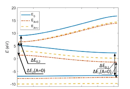
Figure 6. The dispersive curves for the first and second bands: solid line - non-perturbated,
dashed-doted – perturbated solution with A = 0 (CP), dashed - perturbated solution with A = π (IP) In Figure 6 the calculated dispersive curves for non-perturbated and perturbated (A = 0, i.e., commensurate phase, and A ≠ 0 – incommensurate phase) are presented. As one can see, the addition of commensurate perturbation leads to shift of dispersive curves and to the change of band gaps. Firstly, it should be noted that the presence of the perturbated potential leads to shift of the dispersive curves down. Nevertheless, presence of the perturbation can lead to increase or to decrease of the bandgap. As an example, the presence of commensurate phase decreases the first band gap, while the incommensurate phase with A ≠ 0 increases it. Contrary situation is observed
12
for the second bandgap – the commensurate phase leads to increase of the bandgap value, and the incommensurate phase with considered amplitude decreases it.
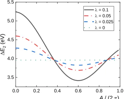
Let us further focus on the consideration of the second bandgap, where the general trend of decreasing of bandgap with the amplitude of incommensurability is expected. Figure 7 shows the dependence of the second band gap on the amplitude of the incommensurability for different values of the perturbation magnitude. As one can see, the bandgap decreases with the λ for the case of commensurability (A = 0). For each value of λ, the band gap monotonically decreases with the A until it reaches the value at which the averaging acting of phase term (∆𝜙 = 𝐴 cos(2𝜋(𝑥 + 𝑏)/𝑐) in Eq. (1) is in antiphase to the unperturbed potential. The maximum reduction of the bandgap of IP respectively to CP is 1.7 eV for the case of λ = 0.1. Additionally, it should be noted that due to the symmetry of the perturbation, the rate of change of the bandgap with A is small close to A = 0, and it increases with the rise of A and slows down in vicinity of the minimum. Therefore, the effect of the incommensurability starts to be more significant after some threshold value of A. According to the model this threshold value depends on the λ, and for the maximum considered value (λ = 0.1), it may be estimated as A = 0.1.
Figure 7. The dependence of the second band gap on the amplitude of the incommensurability
The amplitude A which determines the value of incommensurate term in the total potential in fact characterizes the order parameter in the IP. Then an increase the order parameter in IP at cooling from 214 K to 197 K correlates with an increase the amplitude A,[1] and consequently, correlates with a decrease the band gap width in the temperature region of the IP existence. At IP – CP PT (197 K) amplitude A → 0 and the band gap width increases again. Thus, the increase of conductivity on cooling from 214 K to 197 K and its decrease at further cooling can be associated with the changes of the band gap width when IP appears and decays. Аt first glance the
0.0 0.2 0.4 0.6 0.8 1.0 3.5 4.0 4.5 5.0 5.5 E2 (e V) A / (2 ) = 0.1 = 0.05 = 0.025 = 0
13
electron hopping mechanism of conductivity along localized states near the Fermi level is not directly related with the width band gap.
But the perturbation of energy diagrams and band gap due to the presence of IP phase leads to the modification of the hopping probability between two localized sites, which leads to modification of the involved in Mott equation. Specifically, the modifications of energy distribution results in variation of the energy of separation defining the probability in the case of equal-distance localization sites positions.[23] We hope the proposed model will stimulate more complete calculations the effect of incommensurability on the conductivity of TlInS2 crystals.
5. Conclusions
The conductivity of both unirradiated and irradiated TlInS2 crystals of the C and 2C polytypes decreases on cooling in temperature range of 100 – 300 K. But for samples of the C-polytype in the temperature range of the existence of incommensurate phase (197 – 214 K) an increase of conductivity is observed, which is absent for samples of the 2C-polytype. The conductivity of samples irradiated by X-rays increases in proportion to the absorbed dose. In the temperature range of ≈ 125 – 175 K the mechanism of hopping conductivity with variable hopping length is realized for both polytypes. Based on the Mott equation, the densities of localized states near the Fermi level were determined. Using the one-dimensional Kroning-Penney model, it is shown that the addition of an incommensurate periodic potential to the rectangular lattice potential leads to a shift of the dispersion dependences, while the gap of second band decreases with increasing amplitude of the incommensurate potential.
References
[1] S. Kashida, Y. Kobayashi. X-ray study of the incommensurate phase of TlInS2. J. Phys.: Cond. Matter. 1999, 11, 1027. doi.org/10.1088/0953-8984/11/4/010.
[2] A. M. Panich. Electronic properties and phase transitions in low-dimensional semiconductors. J. Phys.: Cond. Matter. 2008, 20, 293202. doi.org/10.1088/0953-8984/20/29/293202.
[3] A.M. Panich, R.M. Sardarly. Physical Properties of the Low-Dimensional A3B6 and A3B3C Compounds. Nova Science Publishers, New York, USA, 2010, 287 p. ISBN: 978-1-60876-120-3.
[4] I. Martynyuk-Lototska, I. Trach, O. Kokhan and R. Vlokh. Efficient acousto-optic crystal, TlInS2: acoustic and elastic anisotropy. Applied Opt. 2017, 56, 3179. doi.org/10.1364/AO.56.003179.
[5] A. Say, I. Martynyuk-Lototska, D. Adamenko, A. Pogodin, O. Kokhan and R. Vlokh. Thermal expansion anisotropy of β-TlInS2 crystals in the course of phase transitions. Phase Trans. 2018, 91, 1. doi.org/10.1080/01411594.2017.1341983.
[6] A. M. Panich, D. Mogilyansky, and R. Sardarly. Phase transitions and incommensurability in the layered semiconductor TlInS2—an NMR study. J. Phys.s: Cond. Matter..2012, 4, 135901. doi.org/10.1088/0953-8984/24/13/135901.
14
[7] Borovoi N.A., Gololobov,Y.P. Effect of a periodic temperature variation on the properties of TlGaSe2 crystals. Phys. Sol. State. 1997, 39, 1474. https://doi.org/10.1134/1.1130101. [8] S. Vakhrushev, V. Zhdanova, B. Kvyatkovskii. Incommensurate phase transition in TlInS2
crystal. JETF Let (Rus). 1984, 39, 245.
[9] A. V. Salnik, Y. P. Gololobov, N. A. Borovoy. The incommensurate phase transformation in TlInS2 ferroelectric. Ferroelectrics. 2015, 484, 62.
doi.org/10.1080/00150193.2015.1059716.
[10] Alekperov O.Z. and Nadjafov A. I. Dielectric anomalies in monoclinic TlInS2 polytypes. Inorg. Mater. 2004, 40, 1248. doi.org/10.1007/s10789-005-0055-7.
[11] Alekperov, O.Z. and Nadzhafov, A.I. Polytypes of monoclinic TlInS2. Inorg. Mater. 2009, 45, 2009. doi.org/10.1134/S0020168509010026.
[12] N. A. Borovoi, Yu. P. Gololobov, A. N. Gorb and G.L. Isaenko. On the Ferroelectric Phase Transition in Polytypes of β-TlInS2 Crystals. Phys. Sol. State. 2008, 50, 1946. doi.org/10.1134/S1063783408100260.
[13] Mustafaeva S.N., Asadov, M.M Ismaĭlov, A.A. Effect of gamma irradiation on the dielectric properties and electrical conductivity of the TlInS2 single crystal. Phys. Sol. State. 2009, 51, 2269. doi.org/10.1134/S1063783409110122.
[14] M.M. El-Nahass, H.A.M. Alin, E.F.M. El-Zaidia. Characteristics of dielectric properties and conduction mechanism of TlInS2:Cu single crystals. Physica B. 2013, 431, 54. doi.org/10.1016/j.physb.2013.08.035
[15] Sheleg A.U., Gurtovoi V.G., Shevtsova V.V., Mustafaeva S.N. and Kerimova E.M.. Effect of ionizing radiation on the dielectric characteristics of TlInS2 and TlGaS2 single crystals. Phys. Sol. State. 2012, 54, 1870. doi.org/10.1134/S1063783412090284.
[16] Mustafaeva, S.N., Aliev, V.A. and Asadov, M.M. Investigation of dc hopping conduction in TlGaS2 and TlInS2 single crystals. Phys. Sol. State. 1998, 40, 561. doi.org/10.1134/1.1130352.
[17] N. F. Mott, E.A. Davis. Electron Processes in Non-Crystalline materials. Oxford University Press, Oxford, England, 2012.
[18] Hubbell J.H., Seltzer S.M. Tables of X-Ray Mass Attenuation Coefficients and Mass Energy-Absorption Coefficients from 1 keV to 20 MeV for Elements Z = 1 to 92 and 48 Additional Substances of Dosimetric Interest. NIST Stand. Ref. Dat. 2004, 126.
http://www.nist.gov/pml/data/xraycoef/
[19] Oktay Alekperov, Nazim Mamedov, Nuru Safarov, Vagif Gasumov and Arzu Nadjafov. γ-Radiation Stimulated Structural Transition of Monoclinic TlInS2 to Hexagonal Phase. Jpn. J. Appl. Phys. 2011, 50, 05FD05. doi.org/10.1143/JJAP.50.05FD05. [20] Klinger M I, Lushchik Ch B, Mashovets T V G A Kholodar', M K Sheĭnkman and M A
Élango. Defect formation in solids by decay of electronic excitations. Sov. Phys. Usp. 1985, 28, 994. doi.org/10.1070/PU1985v028n11ABEH003977.
[21] R. De L. Kronig and William George Penney. Quantum mechanics of electrons in crystal lattices. Proc. Royal Society A. 1931, 131, 499. doi.org/10.1098/rspa.1931.0019.
[22] Frank Szmulowicz. Kronig-Penney model: a new solution. Eur. J. Phys. 1997, 18, 392. doi.org/10.1088/0143-0807/18/5/015.
[23] N. Apsley, H. P. Hugles. Temperature- and field-dependence of hopping conduction in disordered systems. Phylosoph. Mag. 1974, 30, 963.