HAL Id: hal-03030828
https://hal.archives-ouvertes.fr/hal-03030828
Submitted on 7 Dec 2020
HAL is a multi-disciplinary open access
archive for the deposit and dissemination of
sci-entific research documents, whether they are
pub-lished or not. The documents may come from
teaching and research institutions in France or
abroad, or from public or private research centers.
L’archive ouverte pluridisciplinaire HAL, est
destinée au dépôt et à la diffusion de documents
scientifiques de niveau recherche, publiés ou non,
émanant des établissements d’enseignement et de
recherche français ou étrangers, des laboratoires
publics ou privés.
Measuring the surface bonding energy: A comparison
between the classical double-cantilever beam experiment
and its nanoscale analog
K. Pantzas, F. Fournel, A. Talneau, G. Patriarche, E. Le Bourhis
To cite this version:
K. Pantzas, F. Fournel, A. Talneau, G. Patriarche, E. Le Bourhis. Measuring the surface bonding
energy: A comparison between the classical double-cantilever beam experiment and its nanoscale
analog. AIP Advances, American Institute of Physics- AIP Publishing LLC, 2020, 10 (4), pp.045006.
�10.1063/1.5143843�. �hal-03030828�
A comparison between the classical
double-cantilever beam experiment and its
nanoscale analog
Cite as: AIP Advances 10, 045006 (2020); https://doi.org/10.1063/1.5143843
Submitted: 14 January 2020 . Accepted: 12 March 2020 . Published Online: 02 April 2020 K. Pantzas, F. Fournel, A. Talneau, G. Patriarche, and E. Le Bourhis
COLLECTIONS
Paper published as part of the special topic on Chemical Physics, Energy, Fluids and Plasmas, Materials Science
and Mathematical Physics
ARTICLES YOU MAY BE INTERESTED IN
Improved compensation and measurement of the magnetic gradients in an atomic vapor
cell
AIP Advances
10, 045002 (2020);
https://doi.org/10.1063/1.5127032
Asymmetric propagation of spoof surface plasmons along doubly corrugated metal
surfaces
AIP Advances
10, 045005 (2020);
https://doi.org/10.1063/1.5131326
Core loss calculation for power electronics converter excitation from a sinusoidal excited
core loss data
AIP Advances
ARTICLE scitation.org/journal/advMeasuring the surface bonding energy:
A comparison between the classical
double-cantilever beam experiment
and its nanoscale analog
Cite as: AIP Advances 10, 045006 (2020);doi: 10.1063/1.5143843
Submitted: 14 January 2020 • Accepted: 12 March 2020 • Published Online: 2 April 2020
K. Pantzas,1,a) F. Fournel,2,3 A. Talneau,1 G. Patriarche,1 and E. Le Bourhis4 AFFILIATIONS
1Centre de Nanosciences et de Nanotechnologies, C2N UMR 9001, CNRS - Université Paris-Sud - Université Paris-Saclay,
F-91120 Palaiseau, France
2CEA LETI, Minatec Campus, F-38000 Grenoble, France 3Université Grenoble Alpes, F-38000 Grenoble, France
4Institut P’, CNRS - Université de Poitiers - ENSMA - UPR 3346, SP2MI, F-86962 Futuroscope Chasseneuil Cedex, France a)Author to whom correspondence should be addressed:konstantinos.pantzas@c2n.upsaclay.fr
ABSTRACT
Two experimental implementations of the double-cantilever beam experiment, developed to measure the bonding energy in wafer-bonded semiconductors, are compared for the first time. The comparison is carried out in two material combinations relevant to microelectronics and silicon photonics: Si on an insulator and InP on Si. Although the two implementations differ in the scale of the measured sample area, the measurement conditions, and the step in the fabrication process at which they are applied, they are shown to yield the same values for bonding energy within experimental errors. Both techniques also show the same trend in the evolution of bonding energy when the samples are subjected to annealing.
© 2020 Author(s). All article content, except where otherwise noted, is licensed under a Creative Commons Attribution (CC BY) license (http://creativecommons.org/licenses/by/4.0/).https://doi.org/10.1063/1.5143843., s
I. INTRODUCTION
Semiconductor-wafer direct bonding is a well-established and mature technology for tightly integrating heterogeneous materi-als, without high defect densities typically associated with hetero-epitaxy.1As such, it has found many applications in the semiconduc-tor industry. Foremost among these applications are buried oxides for microelectronics1and integration of thin III-V membranes for the fabrication of active optical components on silicon-based pho-tonic integrated circuits (PICs).2,3The robustness of devices fabri-cated from wafer-bonded semiconductor stacks is directly related to the strength of the bonded interface. Only covalent bonding at the interface ensures the mechanical, chemical, and thermal stability of the end device over its lifetime. Several processing steps, including wafer preparation, the bonding process itself, and
subsequent annealing, are required to ensure that enough covalent bonds are reconstructed at the bonding interface. Over the years, a variety of mechanical tests have been developed to measure the bonding energy at various stages of the process and optimize these steps.
Owing to the simplicity of its implementation, the industry-standard test is the double-cantilever beam (DCB) experiment under fixed displacement, also known as the “razor-blade” or “crack-opening” experiment. In this experiment, a thin razor blade is inserted between two wafers, imposing a fixed separation between the two beams. The torque imposed by this separation is balanced by debonding the two wafers over a certain length along the bonded interface.4–6This is illustrated inFig. 1(a). A variety of models can then be used to obtain a measure of the surface bonding energy from the opening δ imposed by the razor blade and the debonding crack
AIP Advances 10, 045006 (2020); doi: 10.1063/1.5143843 10, 045006-1
FIG. 1. Schematics of (a) the classic double-cantilever beam experiment and (b) its nanoscale equivalent. In the case of the classic DCB, a thin razor blade is inserted
between the two bonded wafers. The razor blade imposes an openingδ and propagates a debonding crack at length L. In the case of the nano-DCB experiment, the thin
membrane obtained after wafer bonding and removal of one of the wafers is probed using instrumented nano-indentation. The area of the membrane that is immediately under or near the indenter is plastically displaced. This displacement creates a torque that, far from the indented region, debonds the membrane from the underlying substrate. The elastically debonded part of the membrane is again held at a heightδ and the debonding crack propagates for length L.
lengthL. The DCB experiment has proven to be highly reliable and well-suited for wafer-scale measurements of surface bonding energy. The DCB experiment, however, requires the preparation of a dedi-cated sample from the bonded wafers, typically a beam 20 mm wide and 50 mm long. This need for a dedicated sample is incompati-ble with the typical sizes of individual PICs in silicon photonics that are often smaller by at least two orders of magnitude and frequently assembled using pick and place. A further limitation of the exper-iment when working with silicon oxide is that it needs to be car-ried in a controlled, anhydrous atmosphere as the debonding crack continues to propagate in the presence of water vapor due to the hydroxylation of the interface.7
In a recent contribution, the authors presented a nano-scale alternative to the experiment that combined instrumented nano-indentation and atomic force microscopy (AFM) to locally debond a membrane of a semiconductor transferred to Si using wafer bond-ing.8–10The configuration of this nano-DCB experiment is schemat-ically depicted in Fig. 1(b). In this configuration, the area of the membrane that is immediately under or near the indenter is plasti-cally deformed. The induced displacement creates a torque that, far from the indented region, debonds the membrane from the under-lying substrate. The elastically debonded part of the membrane is again held at a height δ, and the debonding crack propagates over a lengthL. The nano-DCB experiment requires a significantly smaller surface and can be carried out even after full processing of an InP on Si PIC, as well as throughout the PIC’s lifetime. Nevertheless, the nano-DCB experiment provides sampling of the surface bond-ing energy over a small area. Assessbond-ing the surface bondbond-ing energy of larger surfaces requires sampling several areas, a process that can be quite cumbersome, as it relies on slow probe-tip techniques.
It becomes, therefore, apparent that these two techniques can be highly complementary, provided they are shown to yield similar results on the same samples. As of yet, no attempt has been made to compare the two experiments. This is the purpose of the present contribution. The comparison presented here is based on the two main bonded materials in use today in the semiconductor industry: InP on Si and Si on insulator (SOI). The article is structured as fol-lows: First, the models used to measure the surface bonding energy are outlined, more specifically on how they apply in the two types of experiments. Then, the sample fabrication and experimental proto-col for each measurement are described. Finally, results from both techniques are presented and compared for the two types of bonded materials.
II. THEORY
The DCB is a well-studied experiment in the field of microme-chanics, and an exhaustive treatment of the subject is available in a variety of textbooks, for instance, Ref.11. Two types of bound-ary conditions can be considered: fixed displacement between the cantilever beams or fixed load at the ends of the beams. In both the standard and the nano-DCB experiments considered in the present contribution, the boundary conditions suppose a fixed displacement δ. The load induced by this displacement is balanced by a debond-ing crack of lengthL. These two quantities, measured experimen-tally, are linked to the surface bonding energy through a variety of models.4,12–14
Using elastic theory and making the simplest assumptions— symmetric beams, isotropic materials, zero stress at the crack tip— the surface bonding energyG relates to the two experimental quan-tities δ and L as follows:
G = 3 16
Eδ2h3
(1 − ν)L4, (1)
whereE and ν are the isotropic Young’s modulus and Poisson’s ratio of the material of the beams, respectively, andh is the beam thick-ness, i.e., the thickness of the bonded wafers. In practice, however, more refined models are required to yield precise and reproducible results.7,10These models take into account factors such as beams of dissimilar materials and/or thicknesses, material anisotropy, and/or elasto-plastic bending. The two types of DCB experiments that are compared in the present case rely on two different models that are described in greater detail below. Although the two models are dif-ferent, they have been known to yield results that, in practice, differ by less than 1%.11
A. Standard DCB experiment
For the standard DCB experiment, the formalism proposed by El Zein and Reijsnider is used.14This formalism accounts for the anisotropy of semiconductor materials. In the general case of the asymmetric DCB, the surface bonding energy GEZ is given
by GEZ=3 8 δ2 L4 β1,11/h31+ βSi,11/h3Si [β1,11/h31(1 − Δ1)+ βSi,11/h3Si(1 − ΔSi)]2 , (2)
AIP Advances
ARTICLE scitation.org/journal/adv with Δngiven by Δn= βn,26h 3 i 8βn,11L3 , (3) where βn,ijis βn,ij=Sn,ij− Sn,i3Sn,j3 Sn,33 . (4)Here,Sn,ijandhnrepresent thei, j component of the
compli-ance vector of materialn and its thickness, respectively. B. Nano-DCB experiment
In the case of the nano-DCB experiment, the model of Gillis and Gilman12is used. This semi-empirical model accounts for the elastic deformation of the bonded stack beyond the debonding crack tip. For the δ, L pairs considered in the nano-DCB, this cannot be neglected as it can give an error of as much as 50%.11In the general case of the asymmetric DCB, where one beam is, for instance, InP, and the second is Si, δ and L relate to the surface bonding energy GGGthrough the following equation:
GGG=3δ 2 8L4 F21/E1h31+F22/E2h32 (F3 1/E1h31+F32/E2h32) 2, (5) where Fn=1 + 3chn L + 3 5(1 + νn) h2n L2. (6)
In Eqs.(5)and(6),Enrepresents Young’s modulus,hnis the
thickness, and νnis the Poisson ratio of materialn, respectively.
In summary, Eq.(2)is applied to (δ, L) measured from the razor-blade experiment and Eq.(5)to the sets measured from the nano-DCB experiment. The measurement and corrections required for the two experimental variables δ and L depend on the type of experiment that is carried out. They are explained in detail for each of the two types of experiment in Sec.III. Material parameters for all materials and for both types of experiments are taken from Ref.15.
III. EXPERIMENT
The two techniques discussed in the present contribution are compared on two types of wafer-bonded stacks relevant to the semi-conductor industry, namely, InP on insulator (InPOI) and Si on insulator (SOI). Fabrication details for both types of samples are given in this section, followed by experimental details on the two types of measurements.
A. Sample fabrication
The two types of samples under consideration here are InP bonded to SiO2on Si (InPOI) and Si bonded to SiO2on Si (SOI–Si).
Both types of samples are fabricated using hydrophilic direct bond-ing.7 In the InPOI samples, the bottom half of the bonded stacks consists of (001)-oriented, 200 mm silicon wafers with a thickness of 725 μm. These wafers were thermally oxidized in water vapor at 950○C to form 150 nm thick SiO
2layers at the surface. For the
top half in InPOI stacks, (001) oriented, 50 mm InP wafers with a
thickness of 300 μm were used. A 450 nm InP membrane had been previously grown on an InGaAs etch-stop layer on these substrates using MOCVD. The surface of these wafers was then coated with 50 nm of SiO2and deposited using plasma-enhanced chemical vapor
deposition. In the SOI–Si samples, the bottom half of the bonded stack is the same as that of the InPOI samples. The top half is an SOI wafer with a 150 nm thick (001)-oriented Si membrane on top.
Prior to bonding, all samples were chemically cleaned. Wafers were aligned along the primary flat, and direct wafer bonding was then immediately performed at room temperature under an ambient atmosphere. The InPOI stacks were then annealed at 300○
C. Three different sets of SOI–Si stacks were annealed at three different tem-peratures 200○C, 300○C, and 400○C. All samples were then diced to
produce 20 mm wide beams. One beam per sample was set aside for the standard DCB experiment under an anhydrous atmosphere. In the remaining beams, the top wafer—either InPOI or SOI–Si—and a combination of mechanical thinning and chemical etching was used to produce two types of samples: 450 nm thick InP membranes on 200 nm SiO2on 725 μm Si (InPOI) and 150 nm thick Si membranes,
on 150 nm SiO2on 725 μm Si (SOI–Si).
Prior to DCB experiments, cross sections for transmission electron microscopy were prepared from both types of samples. The cross sections were prepared using focused ion beam (FIB) etching and ion milling. Prior to FIB etching, the samples were coated with a 50 nm thick carbon layer to protect the sample sur-face. The cross sections were observed in an aberration-corrected JEOL 2200FS and an FEI TITAN microscope, both operating at 200 keV.Figure 2shows high-angle annular dark field (HAADF)-STEM micrographs of cross sections of the two types of samples after bonding and thinning. Interfaces between the various materials are atomically flat and contain no voids, a strong indication of robust bonding.
B. Double-cantilever beam experiments
In the standard DCB experiment, a razor blade is inserted between the two bonded wafers inside a glove box, containing less than 1 ppm of water vapor, filled with anhydrous nitrogen. The razor blade is 330 μm thick and is actuated using a step motor with a typ-ical speed of 300 μm s−1and an acceleration/deceleration of 1000 μm s−2. The blade is inserted far enough to go beyond the wafer level, ensuring accurate measurements (seeFig. 3). This razor blade fixes δ at a value of 330 μm.
The debonding length is measured using a 5 megapixel CMOS camera placed above the beam that records the signal transmitted from an infrared (IR) source placed below the beam but outside of the glove box in order to keep a constant temperature inside the con-fined glove box atmosphere. The measured debonding crack length Lintis between the blade tip and the air-wedge interference fringes
observed near the crack tip. This length is then corrected for the por-tion of the blade that penetrates the beamLband also for the portion
of the debonding crack beyond the first optical interference fringe and the crack tipLIR, as discussed in Ref.7. In this reference, it is
shown that the total debonding crack lengthL is a solution to the following cubic polynomial equation:
z3−3L 2 m 4Λ2z − L3m 4Λ3+ L3m 2Λ− 3Lm 8ΛB1− 1 8B2=0, (7)
AIP Advances 10, 045006 (2020); doi: 10.1063/1.5143843 10, 045006-3
FIG. 2. HAADF-STEM micrographs of the two types of samples after removal of
one of the substrates: (a) 450 nm of InP bonded on Si using 200 nm of SiO2
and (b) 150 nm of Si bonded to Si using 150 nm of SiO2. Both the InP/SiO2and
the Si/SiO2interfaces are abrupt, laterally homogeneous, and contain no voids,
indicating strong bonding.
where Λ is Λ = 1 − λ 4δ, (8) B1is B1=β1,12 /h1+ β2,12/h2 β1,11/h31+ β2,11/h32 , (9)
FIG. 3. Schematic description of the razor-blade experiment, annotated to show
all relevant lengths. The total measured length, Lm, is the sum of a portion of the
blade tip, Lb, the length measured from the tip to the last interference fringe, Lint,
and a correction for the portion of the air-wedge, LIRwhere the separation is below
the diffraction limit at the wavelength used to illuminate the sample.
andB2is
B2= β1,26+ β2,26 β1,11/h31+ β2,11/h32
. (10)
In Eqs.(7)–(10), Lm is the sum ofLint andLb, and λ is the
wavelength of the IR source. The remaining variables were defined previously in Sec.II. The debonding crack lengthL is related to the variablez through
L = z +Lm
2Λ. (11)
A typical experimental curve for the anhydrous razor-blade experiment is shown inFig. 4. The curves in the plot describe the evolution of boding energy and blade position vs measurement time. The blade is inserted at a constant speed over 18 s. After the blade reaches its resting position, a small relaxation is observed, which is reflected by a decrease of 200 mJ m−2in the measured bonding energy. In an anhydrous atmosphere, the bonding energy is constant after this point. All values reported here correspond to the average energy over an observation time of 5 min and starting 30 s after the blade is inserted.
The nano-DCB experiments consist in indenting the top mem-brane in all samples using instrumented nano-indentation and then measuring the surface topography of the area surrounding the indents using atomic force microscopy (AFM). Instrumented nanoindentation was performed using a nanohardness tester from CSM Switzerland using a Berkovich diamond tip. The calibration procedure suggested by Oliver and Pharr16was used to correct the load-frame compliance of the apparatus and the imperfections of the shape of the indenter tip. An indentation load of 10 mN was applied at the surface of the InP membranes, and a load of 5 mN was applied to the thinner Si membranes. These indentation loads have been shown to be the most appropriate ones for 450 nm thick InP membranes. Indeed, although a higher load will induce larger displacements that are easier to measure precisely using AFM, if the
FIG. 4. Typical experimental curves for the anhydrous razor-blade experiment. The
red line with square markers shows the evolution of the surface bonding energy as a function of blade-insertion time. The black line with square markers shows the evolution of the blade position measured as a function of time. Shortly after the insertion of the blade, a small relaxation of the energy can be observed. The bonding energy reported for these experiments is the average energy after at least 30 s.
AIP Advances
ARTICLE scitation.org/journal/advload is too high, the membrane can pierce through, and the upper beam can break off. On each sample, ten indentations were per-formed in a line, with each indentation spaced from the next by 50 μm.
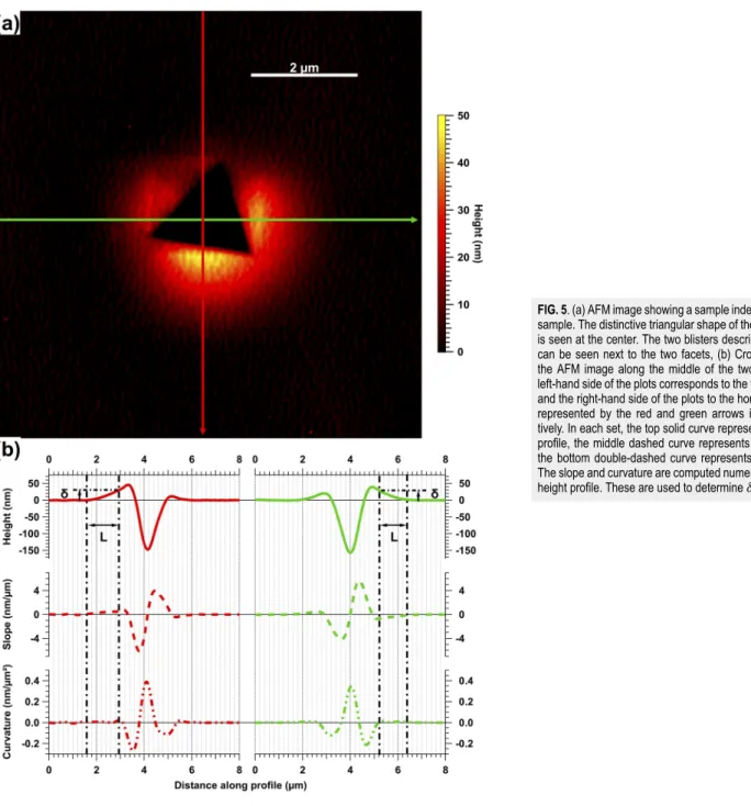
Tapping-mode AFM was used to map the surface topology of the area surrounding the indents.Figure 5shows one such mapping of an indent in InP on Si. The triangular indent left by the Berkovich tip can be seen at the center of the AFM mapping. On two sides, it is flanked by debonding blisters. On the third side, the blister has collapsed. This has previously been shown to be related to the
mechanism through which the blisters are formed.8–10 The InP membrane buckles under the effect of shear stress accumulating in the membrane during the indentation experiment. The shear stress is induced by the torque from the edge component of the disloca-tions that the indenter tip introduces as it penetrates the InP mem-brane and that does not cross the InP/SiO2boundary. In InP,
dis-locations slip along {111} planes, and therefore, the shear stress is projected along the ⟨110⟩ direction. Hence, the smaller the angle θ between the normal to one of the facets and the ⟨110⟩ direction, the higher is the shear stress, propagating the debonding crack lengthL
FIG. 5. (a) AFM image showing a sample indent on an InPOI
sample. The distinctive triangular shape of the Berkovich tip is seen at the center. The two blisters described in the text can be seen next to the two facets, (b) Cross-sections of the AFM image along the middle of the two blisters. The left-hand side of the plots corresponds to the vertical profile, and the right-hand side of the plots to the horizontal profile, represented by the red and green arrows in (a), respec-tively. In each set, the top solid curve represents the height profile, the middle dashed curve represents its slope, and the bottom double-dashed curve represents its curvature. The slope and curvature are computed numerically from the height profile. These are used to determineδ and L.
AIP Advances 10, 045006 (2020); doi: 10.1063/1.5143843 10, 045006-5
farther away from the indenter tip. The blister will reach its equilib-rium height and length when sufficient energy is released from the debonding crack to accommodate the shear stress applied by a given facet of the indenter. For one of the facets, the angle θ is too great, and the blister collapses. The remaining two, however, can be used to determine the surface bonding energy, providing two measurements per indentation.
The crack opening δ and crack length L are determined from cross sections of the mapping along the center of the blisters. The plots inFig. 5(b)show two such cross sections. The left-hand side of the plots (red curves) correspond to the vertical profile, represented by the red arrow in the AFM mapping inFig. 5(a). The right-hand side of the curves (green plots) correspond to the horizontal profile, taken along the green arrow in the AFM mapping inFig. 5(a). In each set of the plots, the solid curve (top) shows the AFM height profile, the dashed curve (middle) shows the slope, and the dotted– dashed curve (bottom) shows the curvature. The slope and curvature are computed numerically from the first and second derivatives of the height profile. The blister lengthLbis determined to beLb=Xb
−X0, whereX0andXbsatisfy
dZ dX(X = X0) ≠0, (12) d2Z dX2(X = X0) =0, (13) and dZ dX(X = Xb) =0, (14) d2Z dX2(X = Xb) =0. (15)
This blister length, measured at the surface of the sample, dif-fers slightly from the length of the debonding crack that propa-gates along the buried bonding interface.10This difference has been attributed to the elastic deformation beyond the debonding crap tip.12,13Gillis and Gilman12proposed the following semi-empirical relation betweenLbandL:
L = Lb−3chInP. (16)
In Eq.(16),hInPrepresents the thickness of the InP membrane,
andc is an empirical factor. A value of 0.63 was proposed by Gillis and Gilman forc, a value given in Ref.10that was found to yield excellent agreement betweenLb, measured using AFM, andL,
mea-sured from a cross section of the same blister using STEM. Finally, the opening, δ, is determined from
δ = Z(Xb). (17)
Using this pair of values (δ, L) determined from the AFM mappings and Eq. (5), one can now deduce the surface bonding energy.
IV. RESULTS AND DISCUSSION
Using the thicknesses reported in Sec.IIIand material param-eters from Ref.15, the surface bonding energyGGGwas measured
from the set of indentations on the InPOI samples. The results are reported in Table I. The average surface bonding energy is 1.28 J m−2, with a standard deviation of 0.14 J m−2, a value that confirms the strong covalent reconstruction of the bonded interface. This average energy is in excellent agreement with measurements provided by the DCB experiment on the same sample, 1.34 J m−2, with a standard deviation of 1.03 J m−2.
These values are close to the average fracture energy in InP, 1.5 J m−2.5Even if the actual bonding energy were higher, neither experiment can measure it as the InP beam would fracture and the debonding crack length from the last dislocation to the crack front would still yield an energy of 1.5 J m−2. It is, therefore, not possible to probe the effect of high temperature annealing on the strengthening of the bonded interface.
To compare the two DCB experiments over a wider range of surface bonding energies, we investigated a second set of sam-ples, namely, the SOI–Si samples discussed previously in Sec.III. Indeed, silicon has a much higher fracture energy; furthermore, a wider range of energies have been reported for various types of SOI bonding methods and annealing temperatures.7,17
Figure 6represents AFM mappings of the indents on the Si membrane for samples annealed at (a) 200○C, (b) 300○C, and (c)
400○
C. Contrary to InP, a blister is present next to each facet of the indent. This is the result of the different behavior of Si under instrumented indentation. Indeed, it has been well documented that Si becomes amorphous under the indenter tip. No dislocation slip beyond the amorphous-Si/crystalline-Si was detected, and they do not collapse the third blister. Aside from this difference in the plas-ticity of Si and InP, the debonding mechanism is the same, and elastic debonding still occurs beneath the blister, allowing one to apply the formalism described in Sec.II A.
TABLE I. Summary of the nano-DCB measurements on the InPOI samples.
δ (nm) Lb(μm) L (μm) GGG(J m−2) 33.4 1.72 0.87 1.46 28.0 1.70 0.85 1.11 38.4 1.83 0.98 1.32 28.2 1.69 0.84 1.16 36.4 1.80 0.95 1.30 30.2 1.72 0.87 1.19 36.0 1.79 0.94 1.33 21.1 1.54 0.69 1.20 38.0 1.88 1.03 1.10 30.1 1.69 0.84 1.33 38.2 1.82 0.97 1.35 28.9 1.72 0.87 1.10 35.8 1.77 0.92 1.40 29.9 1.73 0.88 1.13 34.0 1.70 0.85 1.63 28.3 1.63 0.78 1.48 34.0 1.77 0.92 1.27 29.0 1.71 0.86 1.14 36.1 1.80 0.95 1.29 33.4 1.75 0.90 1.31
AIP Advances
ARTICLE scitation.org/journal/advFIG. 6. AFM mappings of the Si surface of the SOI–Si samples after instrumented
nano-indentation at a load of 10 mN. The three mappings were obtained on sam-ples annealed at (a) 200○C, (b) 300○C, and (c) 400○C. Blisters form on the
facets of the triangular indent left by the Berkovich tip. These blisters occur due to the local debonding of the top Si membrane in the SOI–Si samples. The blisters become visibly smaller with increasing annealing temperature. The surface bond-ing energy deduced from the blisters is 0.88 J m−2, 1.83 J m−2and 3.4 J m−2. A
similar trend is observed in the classical DCB experiment.
TABLE II. Summary of the evolution of the surface bonding energy in the SOI–Si
samples as a function of annealing temperature as determined from the nano-DCB experiment. The last column compares the surface bonding energy using the nano-DCB experiment with that measured on the same sample using the razor-blade experiment.
Ta(○C) δ (nm) L (μm) Ladj(μm) GGG(J m−2) GEZ(J m−2)
200 3.3 0.431 0.148 0.88 0.69
300 2.3 0.372 0.089 1.83 1.96
400 1.7 0.340 0.057 3.40 3.14
A qualitative comparison of the blister size for the various annealing temperatures shows that the higher the annealing temper-ature, the smaller the blisters. This can be seen inFig. 6(c): a green and a blue curve are drawn to show the border between the blister and the non-deformed Si of the same blister at 200○C and 300○C,
respectively. The bonding energies deduced from the AFM map-pings shown inFig. 6are reported inTable II. The values reported in the table clearly show that the surface bonding energy and, by exten-sion, the strength of adhesion increase with an increase in tempera-ture: from below 1 J m−2at 200○
C to more than 3 J m−2at 300○
C. As was the case in InPOI bonding, the surface bonding energies mea-sured for each temperature are less than one standard deviation to the ones measured on the same samples using the anhydrous razor-blade experiment (values reported in the last column ofTable II). In oxide-mediated bonding, such a trend has been reported in the past and has been attributed to an increase in the contact area with covalent bonding. This increase is mainly due to softening of oxide asperities by hydroxylation with water trapped at the bonding interface.17
V. CONCLUSION
In the present contribution, two experimental techniques that measure the surface bonding energy at two different scales have been compared: the classical double-cantilever beam experiment, which gives wafer-scale estimates of the surface bonding energy, and its analog at the nanometric scale, the nano-DCB, which mea-sures the surface bonding energy in an area smaller than a few μm2. The two techniques have been compared on two types of techno-logically relevant materials, InP on an insulator and SOI. Remark-able agreement between the energies measured by both types of experiments has been reported for surface bonding energies up to 4 J m−2. In the future, one can envision profiting of the comple-mentarity of the two techniques, using the razor-blade experiment for wafer-scale measurements early in the fabrication process and the nano-DCB experiment in localized areas of the processed PIC either at the end of the fabrication process or during the PIC’s lifetime.
ACKNOWLEDGMENTS
The authors would like to thankfully acknowledge fund-ing from the CNRS Renatech Network and the ANR Labex TEMPOS.
AIP Advances 10, 045006 (2020); doi: 10.1063/1.5143843 10, 045006-7
REFERENCES 1
Q. Y. Tong and U. Gösele,Semiconductor Wafer Bonding: Science and Technol-ogy, The ECS Series of Texts and Monographs (Wiley, New York, 1999), ISBN: 9780471574811.
2
S. R. Jain, M. N. Sysak, G. Kurczveil, and J. E. Bowers, “Integrated hybrid silicon DFB laser-EAM array using quantum well intermixing,”Opt. Express19, 13692– 13699 (2011).
3
P. Mechet, S. Verstuyft, T. de Vries, T. Spuesens, P. Regreny, D. Van Thourhout, G. Roelkens, and G. Morthier, “Unidirectional III-V microdisk lasers heteroge-neously integrated on SOI,”Opt. Express21(16), 19339–19352 (2013). 4
W. P. Maszara, G. Goetz, A. Caviglia, and J. B. Mckitterick, “Bonding of silicon wafer for silicon-on-insulator,”J. Appl. Phys.64, 4943–4950 (1988).
5D. Pasquariello, M. Camacho, K. Hjort, K. Hjort, L. Dosza, and B. Szentpali, “Evaluation of InP-to-silicon heterobonding,”Mater. Sci. Eng., B80, 134–137 (2001).
6D. Pasquariello and K. Hjort, “Mesa-spacers: Enabling nondestructive measure-ment of surface energy in room temperature wafer bonding,”J. Electrochem. Soc.
147, 2343–2346 (2000).
7F. Fournel, L. Continni, C. Morales, J. Da Fonseca, H. Moriceau, F. Rieutord, A. Barthelemy, and I. Radu, “Measurement of bonding energy in an anhydrous nitrogen atmosphere and its application to silicon direct bonding technology,” J. Appl. Phys.111, 104907 (2012).
8
K. Pantzas, E. Le Bourhis, G. Patriarche, A. Itawi, G. Beaudoin, I. Sagnes, and A. Talneau, “Instrumented nanoindentation and scanning electron
transmission microscopy applied to the study of the adhesion of InP membranes heteroepitaxially bonded to Si,”Eur. Phys. J.: Appl. Phys.65, 20702 (2014). 9K. Pantzas, G. Patriarche, E. Le Bourhis, D. Troadec, A. Itawi, G. Beaudoin, I. Sagnes, and A. Talneau, “Evaluation of the surface bonding energy of an InP membrane bonded oxide-free to Si using instrumented nanoindentation,”Appl. Phys. Lett.103(8), 081901 (2013).
10
K. Pantzas, E. L. Bourhis, G. Patriarche, D. Troadec, G. Beaudoin, A. Itawi, I. Sagnes, and A. Talneau, “Locally measuring the adhesion of InP directly bonded on sub-100 nm patterned Si,”Nanotechnology27, 115707 (2016).
11
D. Maugis,Contact, Adhesion and Rupture of Elastic Solids (Springer, 1997). 12
P. P. Gillis and J. J. Gilman, “Double-cantilever cleavage mode of crack propa-gation,”J. Appl. Phys.35, 647–658 (1964).
13M. F. Kanninen, “An augmented double cantilever beam model for studying crack propagation and arrest,”Int. J. Fract.9, 83–92 (1973).
14
M. S. El-Zein and K. L. Reijsnider, “Evaluation of GIC in a DCB spec-imen using an anisotropic solution,” J. Compos. Technol. Res.10, 151–155 (1988).
15
Ioffe online NSM archive—Properties of InP, May 2013, URL:http://www.ioffe. rssi.ru/SVA/NSM/Semicond/InP/mechanic.html.
16W. C. Oliver and G. M. Pharr, “An improved technique for determining hardness and elastic-modulus using load and displacement sensing indentation experiments,”J. Mater. Res.7, 1564–1583 (1992).
17F. Fournel, C. Martin-Cocher, D. Radisson, V. Larrey, E. Beche, C. Morales, P. A. Delean, F. Rieutord, and H. Moriceau, “Water stress corrosion in bonded structures,”ECS J. Solid State Sci. Technol.4, P124–P130 (2015).