HAL Id: hal-03052868
https://hal.archives-ouvertes.fr/hal-03052868
Submitted on 10 Dec 2020HAL is a multi-disciplinary open access archive for the deposit and dissemination of sci-entific research documents, whether they are pub-lished or not. The documents may come from teaching and research institutions in France or abroad, or from public or private research centers.
L’archive ouverte pluridisciplinaire HAL, est destinée au dépôt et à la diffusion de documents scientifiques de niveau recherche, publiés ou non, émanant des établissements d’enseignement et de recherche français ou étrangers, des laboratoires publics ou privés.
Large scale fabrication of highly emissive nanodiamonds
by chemical vapor deposition with controlled doping by
SiV and GeV centers from a solid source
Mary de Feudis, Alexandre Tallaire, Louis Nicolas, Ovidiu Brinza, Philippe
Goldner, Gabriel Hétet, Fabien Bénédic, Jocelyn Achard
To cite this version:
Mary de Feudis, Alexandre Tallaire, Louis Nicolas, Ovidiu Brinza, Philippe Goldner, et al.. Large scale fabrication of highly emissive nanodiamonds by chemical vapor deposition with controlled doping by SiV and GeV centers from a solid source. Advanced Materials Interfaces, Wiley, 2020, 7 (2), pp.1901408. �10.1002/admi.201901408�. �hal-03052868�
1
Large scale fabrication of highly emissive nanodiamonds by chemical vapor
deposition with controlled doping by SiV and GeV centers from a solid
source.
Mary De Feudis*, Alexandre Tallaire*, Louis Nicolas, Ovidiu Brinza, Philippe Goldner, Gabriel Hétet, Fabien Bénédic, Jocelyn Achard
Dr. M. De Feudis, Dr. O. Brinza, Dr. F. Bénédic, Prof. J. Achard,
Laboratoire des Sciences des Procédés et des Matériaux, CNRS, Université Paris 13, Sorbonne Paris Cité, 93430 Villetaneuse, France
E-mail: mary.defeudis@lspm.cnrs.fr L. Nicolas, Dr. G. Hétet
Laboratoire Pierre Aigrain, Ecole Normale Supérieure, CNRS, PSL Research University, 24 rue Lhomond, 75231 Paris Cedex 05, France
Dr. A. Tallaire, Dr. P. Goldner
Institut de Recherche de Chimie Paris, Chimie ParisTech, CNRS, PSL Research University, 11 rue Pierre et Marie Curie, 75231 Paris Cedex 05, France
E-mail: alexandre.tallaire@chimie-paristech.fr
Keywords: color centers, nanodiamond, chemical vapor deposition, quantum technologies, spectroscopy
ABSTRACT
A new strategy to produce loose chemical vapor deposited Nanodiamonds (ND) without the need of a seeded substrate, and that are intentionally doped by SiV and GeV centres from a solid source is presented. The addition of a low amount of gases such as N2 or O2 during
growth is used as a control knob to finely tune the emission intensity of embedded color centers. NDs with a high brightness and a controllable amount of group IV color centers are eventually obtained. Their optical properties at low temperature indicate that this approach can usefully produce dispersed NDs that can deliver suitable optical performance for quantum technologies.
2
Fluorescent nanodiamonds (ND) are new promising probes that could outperform organic fluorophores for imaging biological systems. NDs exhibit high brightness without photobleaching and are biocompatible non-toxic materials [1]. The nitrogen-vacancy (NV)
defect is one of the most studied color centers in NDs with single photon emission at 637 nm. In addition, room temperature Optically Detected Magnetic Resonance (ODMR) of the spin levels of the negatively charged NV center has opened interesting perspectives beyond the simple fluorescent contrast imaging in order to sense physical parameters at the nanoscale with high sensitivity such as magnetic or electric fields, temperature or pressure [2].
Fluorescent NDs have already demonstrated remarkable performance in various areas including single-photon sources in quantum optics [3], quantitative magnetic field mapping [4],
intra and intercellular molecular processes sensing for biology [5], cancer cell imaging [6] and
effective drug delivery [7].
In addition to the NV, other color centers are being investigated, in particular those involving group IV elements such as the negatively charged Silicon-Vacancy (SiV), Germanium-Vacancy (GeV) as well as Tin-Vacancy (SnV) defects [8],[9],[10]. Although spin
manipulation of group IV defects is not possible at room temperature, they advantageously exhibit emission mostly in their zero phonon line (ZPL) with a much better spectral stability than the NV defect and a much larger Debye-Waller Factor [11]. Single photon emission also
occurs at different frequencies (738 nm, 602 nm and 620 nm respectively), which might be of interest for multicolor bio-labelling [12].
Nowadays, two main approaches exist to synthesize NDs at an industrial scale [13]. By
detonating explosives in a closed vessel, NDs are produced and then scrapped from the reactor walls. Such detonation NDs need to be separated from other non-diamond particles and cleaned to remove contaminants. Specific post-treatments can then be implemented to improve their luminescence properties [14]. Alternatively, grinding micrometric diamond grits
3
conventional high pressure high temperature (HPHT) diamonds are used as powder to mill. Such NDs can contain relevant amount of nitrogen or metallic impurities, in addition the processing could induces mechanical damage and surface contamination and reduces the ultimate optical properties [15]. By intentionally adding impurities during detonation or
conventional HPHT synthesis, specific defects can be produced including group IV color centers [16]. Nevertheless, both these techniques fail to reliably provide highly pure material
with a controllable amount of luminescent defects and good optical properties. Time-consuming post-treatments to remove non-diamond components or to create the desired color centers, such as electron irradiation, are also often required.
More recently, an alternative approach consisting of the direct production of high quality HPHT nanodiamonds by using carbonaceous precursors has been proposed by several research teams with promising results [17],[18],[19],[20]. For example, Bolshedvorski et al. [21]
studied nanondiamonds synthetized by a metal-free HPHT method on the basis of a hydrocarbon-containing growth system. In particular, this group succeeded to produce ultra-small (10 nm) and low-strain diamonds containing an optically active single silicon-vacancy color centers characterized by non-blinking, spectrally narrow emission with narrow distribution of the spectral width. Ekimov et al. [22] as well as Siampour et al. [23] synthetized
diamonds from hydrocarbons under high static pressures conditions ensuring a high incorporation of SiV and GeV colour centres. In particular, the synthesis from organic compounds allowed working simply with two parameters (pressure, temperature) and avoid the presence of metallic impurities and inclusions (which are defects typically related to the diamond synthesis starting from the carbon solution based on transition metals). However, limitations in terms of the particles amount produced per bunch as well as the control of SiV and NV undesired traces were registered.
4
Chemical Vapor Deposition (CVD) has been explored too, and interesting results have been reached for silicon-doped nanodiamonds. In particular, detonation nanodiamonds (a few nm large) are dispersed on a silicon substrate and used as seeds for the diamond growth. By the microwave-plasma exposition, the nanodiamonds grow up to hundreds of nm and incorporate silicon atoms etched away from the substrate. Li et al. [24] characterized such
nanodiamonds showing narrow linewidth for the SiV emitters (325 MHz) and high photostability. Zhou et al. [25] demonstrated the coherent control of a strongly driven optical
transition of a single SiV defect in a CVD nanodiamond, as well as the long and robust coherence time of SiV emission even at high excitation powers. However as main drawback, this technique allows obtaining just a few NDs per run, which are nucleated and strongly attached to seeded substrates [26].
Recently we have proposed a new approach that can lead to the mass production of loose NDs with high crystalline quality by CVD [27]. In this work and for the first time, we
aim at pushing further the potential of this material by showing that specific group IV color centers can be introduced at a controllable level on demand without any purification or irradiation post-treatment. By the CVD technique we succeeded to produce well-faceted and pure monocrystalline NDs in a quantity of a few mg per run together with a contained amount of smaller polycrystalline particles. We eventually demonstrate that bright NDs containing SiV or GeV emitters with promising optical properties can be engineered which paves the way towards their use in bio-applications or for quantum technologies.
NDs were produced by high microwave power plasma assisted CVD using a H2/CH4
gas mixture (94/6) with intentional addition of a small amount of N2 (0 - 5 ppm) or O2 (0 -
0.50 %). The powdery deposit that accumulated on the molybdenum holder maintained at a rather low temperature (< 600 °C) was eventually washed out with ethanol to give a dense NDs suspension. The plasma conditions were optimized to lead to a fairly large amount of
5
NDs with good crystalline quality. We estimate NDs production yield to a few mg per run for a duration of 6 h. The CVD technique gives rise to direct particle homogenous nucleation in the gas phase [27],[28], where thanks the high temperature (3000 K in the plasma core) the
thermal dissociation of the chemical species is promoted [29]. Once synthetized the particles
move onto the cold holder by thermophoresis. The low substrate temperature together with the seeding absence prevents from the continuous polycrystalline diamond film growth. In addition, the particles deposited on the cold molybdenum substrate do not react ensuring a subsequent very easy and quick removal.
By the CVD technique, the doping was ensured placing a small piece (around 20 × 20 mm²) of crystalline Si or Ge onto the holder, near the region where NDs were created. Etching of the material by the high-temperature H2-rich plasma led to incorporation of SiV
and GeV in the produced diamond nanoparticles. Such doping from a solid source advantageously limits the amount of impurities that are introduced in the chamber as compared to gas phase doping. Besides, high purity materials that are commercially available at low cost and easy to handle can be used unlike toxic gases such as silane or germane (SiH4
or GeH4) [30] that require specific dedicated gas lines. The main drawback though comes from
the limited ability to control doping level since the amount of sputtered material from the solid source cannot be easily measured nor varied during growth. In this work, however, we show that the doping level of incorporated impurities can be tuned depending on the growth conditions.
6
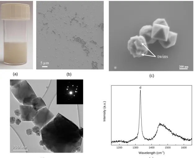
Figure 1. (a) A container with NDs dispersed in ethanol. (b) A representative SEM image of
CVD NDs spin-coated on a Si wafer from the suspension. (c) Enlargement of the SEM image (b) showing clear crystalline facets with some NDs having twins. (d) TEM image from a large single crystalline particle and the corresponding electron diffraction pattern (inset). Smaller polycrystalline nanoparticles are also visible. (e) Typical Raman spectrum obtained with a 473 nm laser from which the diamond Raman peak labelled by the letter “d” is visible together with a broader band attributed to transpolyacetylene.
In Figure 1a the white ND powder dispersed in an ethanol solution is shown. A top-view SEM picture of nanoparticles spin-coated on a silicon wafer is reported (Figure 1b). An enlarged SEM picture (Figure 1c) shows clear crystalline facets with some of them sometimes showing twinning. The particles size is in the range 200 - 400 nm. A closer look at the TEM images (Figure 1d) also supports the fact that under these optimized growth conditions, NDs are well facetted without any obvious graphitic or amorphous contribution. The electron diffraction pattern (inset of Figure 1d) where well-defined diffraction spots from the reciprocal lattice are seen, is indeed indicative of monocrystalline particles [31]. We note
(b) (c) (d) (e) 1200 1300 1400 1500 1600 Int en sity (a .u. ) Wavelength (cm-1 ) d 5 µm (a) twins
7
though that a second group of NDs with a smaller size (30-50 nm) and round-shape were also produced (lower left corner of Figure 1c). These particles were probably nucleated and grown by a different mechanism as confirmed by the TEM characterization (see Supporting Information, Figure S1). These particles exhibit a structure made of aggregated 20 nm large nanocrystals. The corresponding electron diffraction pattern (see Supporting Information,
Figure S1 inset) shows diffraction rings from the reciprocal lattice, which are indicative of
multiple crystalline orientations [31].
In this study, in particular for the luminescence assessment, we essentially focused on the larger single crystalline NDs that bear a stronger potential as fluorescent probes. Raman analysis presented in Figure 1e indeed shows a well-defined diamond Raman peak at 1330 cm-1 with a FWHM of about 10 cm-1, without any obvious graphitic or amorphous
contribution. This highlights that our CVD growth approach is able to mass-produce loose NDs with high crystalline quality. However the diamond peak position present a slight shift respect to the conventional position (1332 cm-1) which can be related, together with a not
negligible full with half maximum, to strain of the CVD nanodiamonds. For completeness, it is useful indicated to presence of an additional band at around 1450 cm-1, which can be
ascribed to vibrations of trans-polyacetylene molecules [32]. This band is typically enhanced in
the CVD diamond materials deposited at low temperatures.
We then investigated the room temperature luminescence properties of in-situ doped NDs. Cathodoluminescence (CL) analysis of NDs produced with different gas phase compositions is presented in Figure 2.
8
Figure 2. Cathodoluminescence of CVD NDs grown with (a) intentional Si doping, (b)
intentional Ge doping. N2 (5 ppm) and O2 (0.25 %) were added to the gas phase during
growth as indicated in the legend. NID stands for non-intentionally doped. Spectra were vertically shifted for clarity. Photoluminescence excited with a 473 nm laser of highly bright NDs containing SiV- centers (c) using 5 ppm N2 additions, and GeV- centers (d) by co-doping
with N2 (5 ppm) and O2 (0.25 %).
In the presence of a nearby solid silicon source, SiV- color centers emitting at 738 nm
were easily incorporated (red curve of Figure 2a). This is consistent with previous reports that have shown that NDs seeded and grown on silicon wafers [33],[34],[35] are contaminated by
impurities from the substrate. In this study though, substrate-free and seedless NDs are easily dispersible and produced in a fairly large amount.
N2 additions as low as 5 ppm during growth dramatically enhanced SiV- emission
leading to bright NDs (blue curve of Figure 2a). We note that low incorporation of nitrogen was detectable from the signature of NV0 color centers in CL. NV- centers might be present
too but are not efficiently excited in CL. Enhancement of SiV- emission by the presence of N2 500 550 600 650 700 750 d Raman peak Wavelength (nm) PL inten sity (a.u.) GeV -(a) (b) (c) (d) 500 550 600 650 700 750 800 850 900 GeV- Ge + N2 + O2 Ge + N2 Ge + O2 Ge only CL intens ity (a.u.) Wavelength (nm) NV0 NID SiV -500 550 600 650 700 750 800 850 d Raman peak SiV -Wavelength (nm) PL inten sity (a.u.) 500 550 600 650 700 750 800 850 900 SiV Si + N2 + O2 Si + N2 Si + O2 Si only CL intens ity (a.u.) Wavelength (nm) NV0
9
is possibly due to the stabilization of this particular negative charge state. Indeed, substitutional nitrogen atoms being deep electron donors in diamond, they may provide free electrons and favor the formation of SiV- centers as already reported both for diamond films
and nanoparticles [8],[36].
Addition of O2 (0.25 %) during growth had the opposite effect, leading to a reduction
of SiV- emission (black and green curves of Figure 2a). Indeed, due to the plasma activity,
the oxygen molecules reach the dissociation conditions and can react easily with the silicon atoms etched from the wafer. The strong bond strength between oxygen – silicon atoms (800 kJ/mol [37]) make this silicon atom unavailable for incorporation into NDs. By increasing
the added O2 amount to 0.5% we confirmed that SiV- emission was further reduced (Figure
S2). This study demonstrates that by this growth method it is possible to tune with high
flexibility the SiV- emissivity by adding an appropriate amount of N2 or O2 even by using a
solid-state doping source.
Growing germanium-doped NDs using only a solid Ge source revealed experimentally more difficult. In particular, the first nanodiamonds were grown using standard plasma conditions together with a germanium solid-wafer and CL investigations showed a very weak emission at 602 nm, characteristic of GeV- centers (black curve of Figure 2b). This emission
was not visible in all NDs. In addition, unintentional doping by Si was sometimes detectable, most likely due to contamination from the silica walls of the reactor chamber. Non Intentionally Doped (NID) SiV- level varied from run to run and depended on the considered
nanoparticle.
Addition of a low amount of N2 (5 ppm) led to a drastic increase of GeV- emission
which became detectable in all the particles and rather intense (blue curve of Figure 2b). However, it also enhanced emission from NV0 and NID SiV-. These latter were in general at
10
GeV- emissivity can be ascribed to the stabilization of this particular negative charge state as
substitutional nitrogen atoms may provide free electrons and favor the formation of those color centers.
Interestingly, addition of O2 (0.25 %) did not seem to affect emission from GeV
-centers but drastically and systematically reduced NID SiV- (red curve of Figure 2b). Since
the oxygen – germanium binding energy (657 kJ/mol [38]) is lower than that for oxygen –
silicon (800 kJ/mol [37]), it may explain that the reduction effect was more obvious for Si than
for Ge impurities. Nevertheless, theoretical investigations taking into account physical-chemical reactions inside the plasma would be needed to fully describe the doping mechanisms involved. Co-doping by O2 and N2 however revealed efficient to promote
emission from GeV- centers at 602 nm while cutting down that from other luminescent
impurities (green curve of Figure 2b).
Based on these optimized growth conditions, the production of bright NDs doped with either SiV- or GeV- centers on demand and with a tunable level was demonstrated. Further
photoluminescence (PL) characterizations performed by a 473 nm laser at room temperature validated these results (see Figure 2c and Figure 2d). The PL spectra were registered on the brightest silicon-doped (Si solid source and 5 ppm N2) and germanium-doped (Ge solid
source, 5 ppm N2 and 0.25 % O2) NDs. The prominent brightness of both color centers is here
easily appreciable using the diamond Raman peak (labelled “d”) as a reference. It is worth saying that no post-treatment (thermal annealing, chemical cleaning or irradiation) was necessary to obtain such a bright and high quality nanodiamonds. Subsequently, the optical properties of CVD NDs were evaluated at low temperature.
11
Figure 3. (a) Confocal raster scan obtained by scanning the sample in front of the microscope
objective. The bright spots show the presence of SiV- centers. (b) SiV- PL spectrum under green laser excitation. Inset: PLE spectrum of the SiV- transition marked by a red arrow. The SiV- center is resonantly excited with 104 nW of laser power. (c) GeV- PL spectrum of one nanodiamond (ND1) doped by Germanium under green off resonant excitation. (d) Photo-luminescence of a germanium doped nanodiamond (ND2) as a function of time.
Figure 3a shows a confocal scan of nanodiamonds containing SiV centers that are cast
on a quartz cover-slip. The presence of single diamond nanoparticles and nanodiamond clusters is manifest from the change in the SiV photoluminescence from one area to another.
Figure 3b shows a photoluminescence spectrum obtained at 10 K. Several narrow peaks can
be observed from 735 nm to 742 nm. Such a spectral dispersion is due to strain inhomogeneity [39]. Given that each peak is well isolated from the other, they most likely all
belong to a single emitter. The true emitter linewidth cannot be measured directly with our spectrometer as it appears to be lower than its resolution. To go beyond, Photoluminescence Excitation (PLE) on the SiV- line marked with a red arrow, using 100 nW of resonant
(a) (b)
12
excitation scanned around the line was performed. PL in the phonon sidebands is measured as the laser frequency is scanned and the spectrum is plotted in Figure 3b. The measured linewidth on this line is 911 MHz, which is about a factor of 3 to 4 times the natural linewidth. This result is very promising as it means that spectral diffusion is low, implying that the symmetry of the SiV- centers is likely to be preserved [40]. Nevertheless, to confirm that,
systematic analyses by a faster PLE read form single SiV centres would be required.
Similar PL spectra have been measured at low temperature using nanodiamonds containing GeV- centers. One of them is shown in Figure 3c. Several spectrally resolved lines
are also visible. Another spectrum is shown in Figure 3d and a good photostability has been measured by monitoring the PL over time. One of the two peaks is very stable both from the point of view of PL rate and spectral diffusion. Unfortunately, PLE on GeV- centers could
not be performed because we lacked a tunable laser at 605 nm. Nevertheless these measured optical properties for both SiV and GeV color centers are extremely promising within the context of quantum technologies that require that a controllable density of luminescent defects with narrow linewidth are incorporated into nanoscale diamonds.
In this work a new approach for high-quality nanodiamond synthesis is proposed. The CVD technique optimization allowed producing well-faceted and pure monocrystalline NDs in a large quantity (a few mg per run) without using any seeded substrate. A small amount of round polycrystalline (30 – 50 large) particles can be also collected after the deposition steps. Importantly, these NDs can be easily dispersed in solution which facilitates their further use or integration in a sensor, or a photonic cavity [41],[42]. With the aim of pushing further the
potential of this method, the incorporation of specific group IV color centers has been demonstrated at a controllable level on demand without any purification or irradiation post-treatment. In addition, a high control of the SiV- and GeV- emissivity has been reached and
13
characterization showed narrow optical lines at cryogenic temperatures, very close to the lifetime limit, and high photostability for both the SiV and GeV centers. Therefore, it is believed that such bright NDs containing SiV or GeV emitters can be engineered so as to open the way to their use in bio-applications or for quantum technologies.
Experimental Section
Nanodiamond growth
Diamond nanoparticles were grown by the Microwave Plasma Assisted Chemical Vapour Deposition (MPACVD) technique. The reactor was a BJS150 model provided by Plassys company. The nanodiamond powder was grown with a gas mixture of H2/CH4 (94/6) under
fixed power and pressure conditions (2.7 kW / 155 mbar). After six hours of deposition, nanodiamonds were collected from a molybdenum substrate holder and dispersed in an ethanol solution.
SEM and TEM observation:
SEM characterizations were carried out by Zeiss Supra VP 40 system. The nanodiamonds were spin coated onto a silicon wafer and analysed under a field effect gun system.
TEM images were registered by a JEOL EM2010 system. The NDs suspension drop was casted onto a carbon TEM grid and analysed by a 200 kV microscope.
Raman/PL
Raman and photoluminescence investigations were performed by a Jobin-Yvon HR800 spectrometer using the 473 nm excitation line at room temperature. The light was focused
14
using a long range 100 X objective. A 1800 l/mm grating was used to disperse light onto a Pelletier cooled CCD camera.
Cathodoluminescence:
CL analysis was carried out using a Horiba HCLUE system connected to a ZEISS EVO MA15 equipped with a high brightness LaB6 filament. The electron beam used to create the
excitation was set at 10 kV and 20 nA. The light was collected by a parabolic mirror and sent out to a spectrometer equipped with a 600 l/mm grating and a Pelletier-cooled CCD camera. The slit width was set to 100 µm.
Spectroscopic analysis
The photoluminescence studies shown in Fig. 3 were realized using a homebuilt confocal microscope at cryogenic temperature with an objective that has a numerical aperture of 0.7 and a closed-cycle cryostat (MyCryoFirm). The sample was attached to a cold finger inside a vacuum chamber and cooled down to 10 K. The emitters were off resonantly excited using 4 mW of laser light at 532 nm laser. The photoluminescence was coupled to a monomode fiber and sent to an avalanche photodiode (SPCL-AQRH-15 Excelitas Technologies) or to an optical spectrometer equipped a grating with 1800 l/mm grating and detected by an Andor camera (DU401A-BVF). SiV- resonant excitation was performed using a narrow line tunable diode laser (Toptica DL Pro). The PL signal was collected on the phonon sidebands and filtered using a long-pass filter (Thorlabs FELH0750) to remove the residual laser signal.
Supporting Information
15
Acknowledgements
We acknowledge the financial support from the Region Ile-de-France in the frame work of DIM SIRTEQ, the European Union’s research and innovation program under grant agreement No 820394 (ASTERIQS), and by the QUANTERA project n°ANR-18-QUAN-0008-02 MICROSENS.
Received: ((will be filled in by the editorial staff)) Revised: ((will be filled in by the editorial staff)) Published online: ((will be filled in by the editorial staff))
16
The table of contents entry should be 50−60 words long and should be written in the present tense and impersonal style (i.e., avoid we). The text should be different from the abstract text.
ToC figure ((Please choose one size: 55 mm broad × 50 mm high or 110 mm
broad × 20 mm high. Please do not use any other dimensions))
CVD plasma technique allows fabricating large scale nanodiamonds. Particles can be easily collected and dispersed in a liquid solution, without needing any treatment. The high technique flexibility makes it possible to dope nanodiamonds by the different IV group elements, such as silicon, in order to obtain incorporated colour centres. As a result SiV centre high emissive can be registered.
Copyright WILEY-VCH Verlag GmbH & Co. KGaA, 69469 Weinheim, Germany, 2018.
CVD plasma synthesis
Liquid dispersed nanodiamonds Nanodiamond photoluminescence
SiV color centers inside a nanodiamond
17
Supporting Information
Large scale fabrication of highly emissive nanodiamonds by chemical vapor
deposition with controlled doping by SiV and GeV centers from a solid
source.
Mary De Feudis*, Alexandre Tallaire*, Louis Nicolas, Ovidiu Brinza, Philippe Goldner, Gabriel Hétet, Fabien Bénédic, Jocelyn Achard
((Please insert your Supporting Information text/figures here. Please note: Supporting Display items, should be referred to as Figure S1, Equation S2, etc., in the main text…)
Figure S1. TEM image from a small polycrystalline particle and the corresponding electron
18
Small round nanodiamonds (30 – 50 nm) can be obtained by CVD technique. SEM investigations show an aggregated nanocrystal structure with multiple orientations, which is confirmed by the diffraction rings from the reciprocal lattice of the electron diffraction pattern.
Figure S2. Cathodoluminescence of silicon-doped CVD NDs grown without oxygen (blue
curve) and with oxygen at the 0.25% and 0.50% (green and red curve, respectively).
Gas composition is a crucial parameter into the CVD technique. For example, by adding different quantity of the oxygen gas during the deposition process, it is possible modulate the negative state charge emissivity of the SiV color center. Cathodoluminescence measurements show the progressive reduction of the SiV- peak (738 nm) as a function of the oxygen quantity
presence. 200 300 400 500 600 700 800 900 1000 Si only Si + O2 (0.25%) Si + O2 (0.5%) CL In ten sity (a .u. ) Wavelength (nm) SiV
-19
REFERENCES
[1] P. Reineck, A. Francis, A. Orth, D. W. M. Lau, R. D. V. Nixon-Luke, I. D. Rastogi, W. A. W. Razali, N. M. Cordina, L. M. Parker, V. K. A. Sreenivasan, L. J. Brown, B. C. Gibson,
Advanced Optical Materials 2016, 4, (10), 1549.
[2] E. Bernardi, R. Nelz, S. Sonusen, E. Neu, Crystals 2017, 7, (5), 124.
[3] I. Aharonovich, S. Castelletto, D. A. Simpson, C. H. Su, A. D. Greentree, S. Prawer,
Reports on Progress in Physics 2011, 74, (7), 076501.
[4] L. Rondin, J.-P. Tetienne, P. Spinicelli, C. D. Savio, K. Karrai, G. Dantelle, A. Thiaville, S. Rohart, J.-F. Roch, V. Jacques, Appl. Phys. Lett. 2012, 100, (15), 153118.
[5] S. Claveau, J.-R. Bertrand, F. Treussart, Micromachines 2018, 9, (5), 247.
[6] M. Chipaux, K. J. van der Laan, S. R. Hemelaar, M. Hasani, T. Zheng, R. Schirhagl,
Small 2018, 14, (24), 1704263.
[7] D. Wang, Y. Li, Z. Tian, R. Cao, B. Yang, Therapeutic Delivery 2014, 5, (5), 511.
[8] H. Zhang, I. Aharonovich, D. R. Glenn, R. Schalek, A. P. Magyar, J. W. Lichtman, E.
L. Hu, R. L. Walsworth, Small 2014, 10, (10), 1908.
[9] J.-W. Fan, I. Cojocaru, J. Becker, I. V. Fedotov, M. H. A. Alkahtani, A. Alajlan, S. Blakley, M. Rezaee, A. Lyamkina, Y. N. Palyanov, Y. M. Borzdov, Y.-P. Yang, A. Zheltikov, P. Hemmer, A. V. Akimov, ACS Photonics 2018, 5, (3), 765.
[10] T. Iwasaki, Y. Miyamoto, T. Taniguchi, P. Siyushev, M. H. Metsch, F. Jelezko, M. Hatano, Physical Review Letters 2017, 119, (25), 253601.
[11] U. Jantzen, A. B. Kurz, D. S. Rudnicki, C. Schäfermeier, K. D. Jahnke, U. L. Andersen, V. A. Davydov, V. N. Agafonov, A. Kubanek, L. J. Rogers, F. Jelezko, New
Journal of Physics 2016, 18, (7), 073036.
[12] L. Dei Cas, S. Zeldin, N. Nunn, M. Torelli, A. I. Shames, A. M. Zaitsev, O. Shenderova, Advanced Functional Materials 2019, 29, (19), 1808362.
[13] N. Nunn, M. Torelli, G. McGuire, O. Shenderova, Current Opinion in Solid State and
Materials Science 2017, 21, (1), 1.
[14] P. Reineck, D. W. M. Lau, E. R. Wilson, K. Fox, M. R. Field, C. Deeleepojananan, V.
N. Mochalin, B. C. Gibson, ACS Nano 2017, 11, (11), 10924.
[15] H. S. Knowles, D. M. Kara, M. Atatüre, Nature Materials 2013, 13, 21.
[16] V. A. Davydov, A. V. Rakhmanina, S. G. Lyapin, I. D. Ilichev, K. N. Boldyrev, A. A.
Shiryaev, V. N. Agafonov, JETP Letters 2014, 99, (10), 585.
[17] H. Alkahtani Masfer, F. Alghannam, L. Jiang, A. Almethen, A. Rampersaud Arfaan, R. Brick, L. Gomes Carmen, O. Scully Marlan, R. Hemmer Philip, in Nanophotonics, Vol. 7, 2018, 1423.
[18] Y. N. Palyanov, I. N. Kupriyanov, A. F. Khokhryakov, Y. M. Borzdov,
CrystEngComm 2017, 19, (31), 4459.
[19] M. J. Crane, A. Petrone, R. A. Beck, M. B. Lim, X. Zhou, X. Li, R. M. Stroud, P. J.
Pauzauskie, Science Advances 2019, 5, (5), eaau6073.
[20] T. Zapata, N. Bennett, V. Struzhkin, Y. Fei, F. Jelezko, J. Biskupek, U. Kaiser, R. Reuter, J. Wrachtrup, F. A. Ghannam, P. Hemmer, arxiv.org/abs/1702.06854 2017.
[21] S. V. Bolshedvorskii, A. I. Zeleneev, V. V. Vorobyov, V. V. Soshenko, O. R. Rubinas, L. A. Zhulikov, P. A. Pivovarov, V. N. Sorokin, A. N. Smolyaninov, L. F. Kulikova, A. S. Garanina, S. G. Lyapin, V. N. Agafonov, R. E. Uzbekov, V. A. Davydov, A. V. Akimov, ACS
Applied Nano Materials 2019, 2, (8), 4765.
[22] E. A. Ekimov, M. V. Kondrin, V. S. Krivobok, A. A. Khomich, I. I. Vlasov, R. A. Khmelnitskiy, T. Iwasaki, M. Hatano, Diam. Relat. Mat. 2019, 93, 75.
[23] H. Siampour, S. Kumar, V. A. Davydov, L. F. Kulikova, V. N. Agafonov, S. I. Bozhevolnyi, Light: Science & Applications 2018, 7, (1), 61.
20
[24] K. Li, Y. Zhou, A. Rasmita, I. Aharonovich, W. B. Gao, Physical Review Applied
2016, 6, (2), 024010.
[25] Y. Zhou, A. Rasmita, K. Li, Q. Xiong, I. Aharonovich, W.-b. Gao, Nature
Communications 2017, 8, (1), 14451.
[26] E. Neu, C. Arend, E. Gross, F. Guldner, C. Hepp, D. Steinmetz, E. Zscherpel, S. Ghodbane, H. Sternschulte, D. Steinmüller-Nethl, Y. Liang, A. Krueger, C. Becher, Appl.
Phys. Lett. 2011, 98, (24), 243107.
[27] A. Tallaire, O. Brinza, M. De Feudis, A. Ferrier, N. Touati, L. Binet, L. Nicolas, T. Delord, G. Hétet, T. Herzig, S. Pezzagna, P. Goldner, J. Achard, ACS Applied Nano Materials
2019, 10.1021/acsanm.9b01395.
[28] A. Kumar, P. Ann Lin, A. Xue, B. Hao, Y. Khin Yap, R. M. Sankaran, Nature
Communications 2013, 4, (1), 2618.
[29] K. Hassouni, F. Silva, A. Gicquel, J. Phys. D 2010, 43, (15), 153001.
[30] A. Bolshakov, V. Ralchenko, V. Sedov, A. Khomich, I. Vlasov, A. Khomich, N. Trofimov, V. Krivobok, S. Nikolaev, R. Khmelnitskii, V. Saraykin, Phys. Stat. Sol. (a) 2015,
212, (11), 2525.
[31] F. Zhang, E. Burkel, Synthesis of Diamond Using Spark Plasma Sintering, Intech Open, London, United Kingdom 2011.
[32] A. M. Zaitsev, Optical Properties of Diamond: A Data Handbook, Springer, 2001.
[33] L. Nicolas, T. Delord, P. Huillery, E. Neu, G. Hétet, AIP Advances 2018, 8, (6), 065102.
[34] B. Tegetmeyer, G. Lewes-Malandrakis, M. Wernet, C. Schreyvogel, N. Lang, T. Yoshikawa, C. E. Nebel, Diam. Relat. Mat. 2016, 65, 87.
[35] C. Arend, P. Appel, J. N. Becker, M. Schmidt, M. Fischer, S. Gsell, M. Schreck, C. Becher, P. Maletinsky, E. Neu, Appl. Phys. Lett. 2016, 108, (6), 063111.
[36] A. T. Collins, M. Kamo, Y. Sato, Journal of Materials Research 1990, 5, (11), 2507.
[37] L. Brewer, G. M. Rosenblatt, Adv. High Temp. Chem. 1969, 2, 1.
[38] L. Brewer, G. M. Rosenblatt, in Advances in High Temperature Chemistry, Vol. 2 (Ed:
L. Eyring), Elsevier, 1969, 1.
[39] S. Meesala, Y.-I. Sohn, B. Pingault, L. Shao, H. A. Atikian, J. Holzgrafe, M. Gündoğan, C. Stavrakas, A. Sipahigil, C. Chia, R. Evans, M. J. Burek, M. Zhang, L. Wu, J. L. Pacheco, J. Abraham, E. Bielejec, M. D. Lukin, M. Atatüre, M. Lončar, Phys.Rev. B 2018, 97, (20), 205444.
[40] E. Neu, C. Hepp, M. Hauschild, S. Gsell, M. Fischer, H. Sternschulte, D. Steinmüller-Nethl, M. Schreck, C. Becher, New Journal of Physics 2013, 15, (4), 043005.
[41] J. Benedikter, H. Kaupp, T. Hümmer, Y. Liang, A. Bommer, C. Becher, A. Krueger, J.
M. Smith, T. W. Hänsch, D. Hunger, Physical Review Applied 2017, 7, (2), 024031.
[42] J. P. Tetienne, T. Hingant, L. Rondin, A. Cavaillès, L. Mayer, G. Dantelle, T. Gacoin, J. Wrachtrup, J. F. Roch, V. Jacques, Phys.Rev. B 2013, 87, (23), 235436.