Remerciements
Tout d'abord et avant tout, je remercie Dieu de m'avoir toujours béni avec les bonnes opportunités que la vie m'a offertes et pour sa guidance, me donnant la force de surmonter tous mes défis.
Cette thèse a été réalisée au sein de l’Institut Carnot CIRIMAT (Centre Interuniversitaire de Recherche et d’Ingénierie des MATériaux) de l’Université Paul Sabatier dans les équipes Oxydes à Valence Mixte et Revêtements et Traitement de Surface. Mes premiers remerciements vont à mes encadrants de thèse : M. Jean-Yves Chane Ching et M. Pierre-Louis Taberna, directeurs de recherche du CNRS au CIRIMAT. Merci de m'avoir guidé et enseigné pendant ces 4 années, de m'avoir donné toute l'aide et l'opportunité de terminer ce doctorat et surtout d'avoir cru en moi. Je remercie également M. Andrea Balocchi, maître de conférences à l'INSA Toulouse, pour toute l'assistance et l'enseignement. De plus, je suis reconnaissant à Lucianna Gama, qui m'a aidé avec l'opportunité de poursuivre un doctorat en France.
Je remercie les deux rapporteurs de mon jury de thèse; Mme Sophie Cassaignon, professeur à l'Université de Sorbonne et M. Frédéric Sauvage, directeur de recherche au Laboratoire de Réactivité et Chimie des Solides, pour leurs commentaires et remarques pertinentes. Je remercie également M. Bruno Jousselme, directeur de recherche au CEA Paris-Saclay et M. Vincent Paillard, professeur à l'Université Paul Sabatier, d'avoir accepté de participer à ce jury de thèse. Je remercie et salue également l'aide apportée par le Conseil national du développement scientifique et technologique - CNPq (agence brésilienne pour la promotion de la science) qui m'a accordé les moyens financiers pour réaliser mon doctorat en France et pour encourager le développement de la recherche scientifique au Brésil.
Je remercie également le laboratoire CIRIMAT de m'avoir accueilli et de m'offrir un environnement agréable et convivial pour mener à bien mes travaux. Je suis particulièrement reconnaissant à Jean Jacques, Marie Claire, Pauline, Vincent, Pierre, Benjaman, Abde, Nabila, Jessie et Murielle qui m'ont aidé pendant ces années et qui ont contribué d'une manière ou d'une autre avec la réalisation de mon travail. Pourtant, j'ai rencontré de chers amis et collègues sur le labo qui m'ont aussi aidé et encouragé, avec qui j'ai échangé des idées et des bonnes soirées pendant ces 4 années: Dasha, Itchy, Xue, Marie, Inthuga, Candida, Romain, Quentin, Assane, Hue, Justine, Marco, Julien, Anthony, Clément et Andreas.
Je remercie à toute ma famille, mes parents et ma sœur Izabelle, qui m'ont toujours et tout le temps soutenu dans tous mes choix et dans les moments difficiles, et qui ont tout fait pour garantir mon bonheur et ma réussite.
Certainement, je suis également reconnaissant à ma famille brésilienne-toulousaine. Mes chers amis qui m'ont encouragé et m'ont donné le sentiment d'être chez moi même loin de la famille: Patricia, Lilaine, Leticia, Paulo, Hans, Gustavo, Natalia, Juliano, Giovanna et tout la troupe brésilienne. Je remercie Violette, avec qui j'ai partagé le lieu que j' ai appellé chez moi et vécu à Toulouse pendant ces 4 années. Je remercie également mes chers amis bré siliens, qui même de loin, étaient présents sur ce parcours, me conseillant et croyant en moi: Roberta, Luanna, Raquel et Gabriela. Et à mes cousines-sœurs Priscila et Samara qui m'ont toujours conseillé et qui sont une de mes sources d'inspiration depuis que je suis petite.
Enfin, je suis extrêmement reconnaissant envers tous ceux qui m'ont aidé direct ou indirectement et qui ont fait partie de mon cheminement vers l'obtention de mon doctorat. Merci beaucoup à tous.
Table of Content
List of Abbreviations……….….11 List of Figures……….………..……..13 List of Tables……….………...23 Introduction ... 25 CHAPTER I ... 33A Solar Water Splitting for Hydrogen Evolution ... 35
A.1 Context ... 35
B Principles of Solar Water Splitting ... 37
B.1 Processes in the photocatalytic water splitting ... 37
B.2 Solar-to-Chemical Using Semiconductors ... 38
B.3 Photoelectrochemical Cell ...46
B.4 Emerging p-type Semiconductors as Photocathodes...50
B.5 2D TMDCs as promising materials for Solar Water Splitting ... 54
C Two-dimensional TMDCs for HER Evolution ... 57
C.1 Crystalline Structure ... 57
C.2 Synthesis routes: bulk to ultrathin films of TMDCs ...58
C.3 Optoelectronic Properties of 2D TMDCs ... 62
D Design of High Performance Photocathode for HER... 66
D.1 Morphology optimization to obtain high surface area photocathodes ... 68
D.2 Surface defects – Main Challenges of the 2D TMDC Materials ...71
D.3 Nanojunctions formed by semiconductor-carbon self-assembly ... 80
D.4 Previous works of TMDC materials for solar water splitting ...84
Summary and Work Strategies ... 91
Bibliographic references ...94
CHAPTER II... 107
Introduction ... 109
II.1 Material Synthesis and Elaboration ... 109
II.1.1 TMDC Nanoflakes Fabrication ... 109
II.1.2 TMDC photo-electrodes fabrication... 112
II.1.3 MoxSy-based co-catalyst fabrication and deposition ... 113
II.2 Material Characterization... 116
II.2.1 Characterizations of Solids ... 116
II.2.2 Characterizations of Solutions ... 123
II.3 Electrochemical Characterizations...124
II.3.1 Photoelectrochemical (PEC) Measurements ... 124
II.3.2 Linear Sweep Voltammetry ... 124
II.3.4 Electrochemical Impedance Spectroscopy (EIS) ... 125
II.3.5 Mott-Schottky model ... 127
II.3.6 Intensity Modulated Photocurrent Spectroscopy (IMPS) ... 129
II.3.7 Incident Photon-to-electron Conversion Efficiency (IPCE) – External Quantum Efficiency ... 131
II.4 Hydrogen measurements ... 133
II.4.1 Gas Chromatography ... 133
II.5 Theoretical Methods ... 134
II.5.1 Density Functional Theory (DFT) Calculations... 134
BIBLIOGRAPHIC REFERENCES ... 135
CHAPTER III ... 137
Introduction ...139
III.1 Elaboration of solvent-exfoliated p-WSe2 nanosheets ...139
III.1.1 Fabrication of p-WSe2 photoelectrodes... 139
III.2 Characterization of as-exfoliated WSe2 films ... 140
III.2.1 Structure-properties of WSe2 nanoflakes ...140
III.2.2Optoelectronic Properties of the p-WSe2 nanoflakes ... 142
III.3 Photoelectrochemical evaluation of 2D p-WSe2 films ...145
III.3.1 Influence of the layer number on photoelectrochemical characteristics of 2D WSe2 films ...146
III.3.2 Enhancement of photo-activity of p-WSe2 based electrodes ... 147
Conclusion ... 150
Bibliography references ... 151
CHAPTER IV... 153
Introduction ...155
IV.1 Mo Thio and Oxo Thio Complexes Catalysts ... 156
IV.1.1 Elaboration of Water Soluble Mo Thio Oxo Thio Complexes ...156
IV.1.2 Identification of Mo Thio and Oxo Thio Complexes formed in aqueous dispersions....156
IV.2 Mo Thio and Oxo-thio complexes catalyst drop casted on FTO substrate and on 2D p-WSe2 photocathodes... 161
IV.2.1 Identification of Mo Thio and Oxo Thio Complexes on FTO substrate ... 161
IV.2.2 Characterization of thio, oxo-thio Mo complexes films drop casted on FTO and WSe2 substrates ... 162
IV.2.3 Contributions in the catalytic activity of drop casted Mo thio complexes on FTO substrate and WSe2 photoelectrodes...164
IV.3 Thio and oxo-thio Mo complexes (MoxSy) catalyst dip coted on 2D p-WSe2 photocathodes ... 168
IV.3.1 Selection of Mo thio oxo-thio complexes species by dip-coating and film formation . 168 IV.3.2 PEC performances of thio, oxo-thio Mo Complexes in 2D Materials ... 168
IV.3.3 Optimization of the photocatalytic activity of Mo thio oxo-thio complexes on WSe2
electrodes ... 172
IV.3.4 Stability of Mo thio oxo-thio complexes-WSe2 photo-electrodes ... 173
IV.3.5 H2 production of Mo thio oxo-thio complexes-WSe2 dip coated on 2D WSe2 photoelectrodes ... 174
IV.3.6 Material characterization of dip coated WSe2 photoelectrodes with Mo thio oxo-thio catalyst film ... ... 175
IV.3.7 Physical properties of Mo thio oxo-thio complexes catalyst film ...178
IV.3.8 Electrochemical evidences of Mo thio-, oxo-thio complexes film as Healing Catalysts for the 2D WSe2 ... 181
IV.3.9 Photoluminescence spectroscopy of 2D WSe2 photoelectrodes with deposited catalyst film ...184
Further insights about the Mo thio, oxo-thio complexes film as healing catalysts...185
Conclusion ... 192
Bibliography references ...193
CHAPTER V ... 197
Introduction ... 199
V.1 Preparation of rGO-WSe2/MoxSy hetero-structures...200
V.1.1 Use of Sb2S3 –SnS2 amorphous colloids as etching template... 200
V.1.2 SnxSbySz colloid surfaces characterization ... 200
V.1.3 Self-assembly of WSe2 nanoflakes, Sb2S3 – SnS2 template and GO nanosheets ... 201
V.1.4 Catalyst deposition on the assembled 3D rGO-WSe2 films ... 204
V.2 Characterization of nanostructured 3D rGO-WSe2 ... 205
V.2.1 Morphology of nanostructured 3D rGO-WSe2... 205
V.2.2 X-ray Diffraction investigation of nanocrystal domains on 3D rGO-WSe2 ... 206
V.2.1 Electrical conductivity of nanostructured 3D rGO-WSe2 films ... 208
V.3 Characterization of hetero-structures composed of self- assembled rGO-WSe2 3D films and MoxSy catalyst ... 210
V.3.1 High Resolution TEM investigation of 3D rGO-WSe2/MoxSy films... 210
V.3.2 High-angle Annular Dark-field STEM on 3D rGO-WSe2/MoxSy hetero-structures ... 211
V.3.3 Surface investigation of 3D rGO-WSe2/MoxSy hetero-structures probed by XPS ... 212
V.4 Photoelectrochemical characterizations of 3D rGO-WSe2/MoxSy hetero-structures. ...217
V.4.1 Photocatalytic activity on bare 3D self-assembled rGO-WSe2 films ... 217
V.4.2 Optimization of the rGO nanosheets ratio for improved charge carrier collect ... 218
V.4.3 Photocatalytic activity of 3D rGO-WSe2/MoxSy hetero-structures... 221
V.4.4 Charge-transfer resistance of 3D rGO-WSe2/MoxSy hetero-structures ... 223
V.4.5 Incident Photon-to-Current Efficiency ... 228
V.5 Healing Properties of the MoxSy complexes catalyst onto 3D rGO-WSe2 films ... ... 230
V.5.2 Investigation of charge transfer and recombination kinetics by IMPS ... 232
Conclusion ... 235
Bibliography references ... 236
Outlook... 239
Introduction ...241
1 Self-assembly of exfoliated p-WS2 films ... 242
1.1 2D p-WS2 nanoflakes fabrication by solvent exfoliation...242
1.2 Self-assembly of WS2 nanoflakes, Sb2S3 – SnS2 template and GO nanosheets ...242
1.3 Fabrication of p-WS2 electrodes and MoxSy catalyst deposition ...242
2 Characterization of high specific surface microstructure made of 2D TMDCs... 243
2.1 Surface area and pore volume of TMDC materials ...243
3 Properties of exfoliated p-WS2 nanosheets: Preliminary results ... 244
3.1 Optical properties of exfoliated p-WS2 thin films ... 244
3.2 Photocatalytic performance of p-WS2 nanoflakes for the HER ... 245
4 Perspectives ... 247
Conclusion ... 248
Bibliographic references ... 249
Conclusion ……….249
List of Abbreviations
HER Hydrogen Evolution Reaction
PEC Photoelectrochemical
NHE Normal Hydrogen Electrode
2D Two-dimensional
TMDC Transition Metal Di-Chalcogenide
rGO Reduced Graphene Oxide
MoxSy Thio, oxo-thio Mo Complexes
FTO Fluor doped Thin Oxide
XRD X-Ray Diffraction
XPS X-Ray Photoelectron Spectroscopy
ESI-MS Electrospray Ionization Mass Spectrometry HRTEM High Resolution Transmission Electron Microscope SEM-FIB Focused Ion Beam Scanning Electron Microscope
HAADF-STEM
High-angle annular dark-field - Scanning transmission electron microscopy
BET Brunauer-Emmett-Teller
PL Photoluminescence
NMR Nuclear Magnetic Resonance
LSV Linear Sweep Voltammetry
EIS Electrochemical Impedance Spectroscopy
IMPS Intensity Modulated Photocurrent Spectroscopy IPCE Incident Photon-to-electron Conversion Efficiency
List of Figures
Figure I - 1: Schematic of the fundamental mechanisms of photocatalytic water splitting [15]. 37 Figure I - 2: Pourbaix diagram for water, including equilibrium regions for water, oxygen and hydrogen [16]. ... 38 Figure I - 3: Generation of bands in solids from atomic orbitals of isolated atoms [17]... 39 Figure I - 4: Schematic diagram of the energy levels of an (a) n-type semiconductor and a (b) p-type semiconductor [17]. ...40 Figure I - 5: Band bending for an (a) n-type semiconductor and a (b) p-type semiconductor in equilibrium with an electrolyte [17]. ... 42 Figure I - 6: Effect of varying the applied potential (E) on the band edges in the interior of an n-type and p-n-type semiconductors [17]... 43 Figure I - 7: Energy bands in a system of two semiconductors chosen to generate opposite photovoltages [21]... 44 Figure I - 8: Band-gap energies and relative band positions of different semiconductors relative to the water oxidation/reduction potential (vs. NHE) [14]... 45 Figure I - 9: Energy vs. crystal momentum for a semiconductor with (a) direct band gap, (b) indirect band gap, showing that an electron cannot shift from the highest-energy state in the valence band to the lowest-energy state in the conduction band. Here, almost all of the energy comes from a photon (vertical arrow), while almost all of the momentum comes from a phonon (horizontal arrow) [26]. ...46 Figure I - 10: (a) Schematic of a single-type PEC cell for water splitting with incident solar illumination [27]. (b) Working principle of single-type PEC using a photoelectrode with a single bandgap energy (Eg) under illumination [29] (adapted image). ... 47
Figure I - 11: (a) Schematic of a ‘wired’-type tandem cell for water splitting with incident solar illumination striking the photoanode and transmitting to the photocathode. (b) Working principle of the tandem cell using a photoanode with bandgap energy Eg1 and a photocathode
with Eg2 (where Eg,1 > Eg,2 ) [27]...48
Figure I - 12: Electron energy scheme of single PEC water splitting using a photoanode. The absorption of a photon (hv) by the semiconductor with a band-gap (Eg) creates an electron-hole
pair with free energy of Δμex [30]. ...48
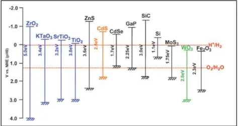
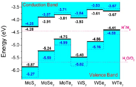
Figure I - 13: Shockley–Queisser limit for a solar cell with a cell temperature at 300 K illuminated by a black body with a surface temperature of 6000 K (black curve) compared to the detailed balance limit for standard solar cell test conditions (Tc = 298.15 K, AM 1.5G). Considering only radiative recombination (green curve), non-radiative recombination that is 10-3 (red curve) and 10-6 (blue curve) times stronger than radiative recombination [33]. ...49 Figure I - 14: The relation between the semiconductor bandgap and the obtained photocurrent under AM 1.5G illumination and IPCE conversion efficiency. *The collected data was based on experimental results of previous works [36], [39], [46], [52], [53], [59], [67], [68]. ... 54 Figure I - 15: Calculated band alignment for MX2 monolayers. The dotted lines indicate the water
reduction (H+/H
2) and oxidation (H2O/O2) potentials. The vacuum level is taken as zero
Figure I - 16: Three-dimensional schematic representation of a typical MX2 structure, with the
chalcogen atoms (X) in yellow and the metal atoms (M) in grey [69]... 57 Figure I - 17: Schematics of the structural polytypes: 2H (hexagonal symmetry, two layers per repeat unit, trigonal prismatic coordination), 3R (rhombohedral symmetry, three layers per repeat unit, trigonal prismatic coordination) and 1T (tetragonal symmetry, one layer per repeat unit, octahedral coordination) [69]. ...58 Figure I - 18: (a) Two kinds of mechanics routes for exfoliating graphite into graphene flakes and the auxiliary route for fragmentation, (b) illustrative procedure of Scotch-tape based micromechanical cleavage of HOPG [79]. ...59 Figure I - 19: Ions (yellow spheres) are intercalated between the layers in a liquid environment, swelling the crystal and weakening the interlayer attraction. Then, agitatio n can completely separate the layers, resulting in an exfoliated dispersion [81]... 60 Figure I - 20: Liquid exfoliation and size selection. (A) Photograph of a typical starting material, WS2 powder, yielding (B) colloidal stable colored dispersions after the exfoliation containing (C)
a mixture of nanosheets with varying lateral sizes and thicknesses. (D) Schematic of the liquid cascade centrifugation with subsequently increasing rotational speeds ω. The supernatant after each step is subjected to another centrifugation at higher centrifugal acceleration. Size-selected nanosheets are collected as sediments [85]. ...62 Figure I - 21: Band-gap energy of thin layers of MoS2. The dashed line represents the indirect band-gap energy of bulk MoS2 [88]. ... 63 Figure I - 22: PL spectra for mono- and bilayer MoS2 samples in the photon energy range from
1.3 to 2.2 eV. Inset: PL QY of thin layers for N = 1–6 [88]... 63 Figure I - 23: Absorption spectra and the PL spectra for a mono and bi-layer of MoS2 [88]. ....64
Figure I - 24: (a) Strategy for improving hematite performance photocurrent density for an idealized hematite photoanode (solid black trace) compared to the typical performance (solid grey trace) under simulated sunlight, and the expected effects of improving the surface chemistry and the morphology [98]; (b) Photocurrent (solid lines) and dark current (dotted lines) vs. applied voltage curves of control (red) and encapsulated (blue) hematite photoanodes after annealing step under simulated solar light in 1M NaOH electrolyte [99]. ... 66 Figure I - 25: Top view SEM images for air-annealed CdS (a,b,c) and Argon-annealed CZTS (d,e) nanoparticle thin films prepared from solutions containing nitrocellulose weight fractions (wt) as indicated. (f) shows a cross section image of the film in (e). All films were annealed at 300°C [115]. ... 69 Figure I - 26: (a) Top-view and (b) side-view SEM images of nanoporous BiVO4 prepared using
DMSO/VO(acac)2 [116]... 69
Figure I - 27: (a) Atomic-resolution annular dark field (ADF) images showing different types of vacancy and vacancy complexes in MoS2 monolayers [126]. (b) High-resolution transmission
electron microscopy (HRTEM) image and (c) structural model showing a single vacancy line in MoS2 monolayers [128]. Via [123] ... 72
Figure I 28: Schematic illustration of the band structure for a surface passivation layer on p -type semiconductor [104]. ... 74 Figure I - 29: (a) WSe2 prepared by exfoliating as-received power, which likely contains Se
vacancies both at the exposed flake edges and internally in the few-layer flakes. (b) WSe2
surfactant is suggested for the filling of the exposed edge vacancies to give the WSe2 samples
(panels c and d) [68]... 75 Figure I - 30: Comparison of an n-type semiconductor photoanode with (a) surface defect states in the band structure, which lead to high charge recombination and inefficient water oxidation by the photogenerated holes; (b) application of an OER catalyst layer, which pro motes facile hole transfer across the interface to the catalyst for improving water oxidation [104]. ... 77 Figure I - 31: J−E behavior of p-WSe2 photoelectrodes from aqueous pH 4.2 electrolyte without
catalyst coating and with Ru, Pt, or Ru/Pt coatings, respectively [67]. ...78 Figure I - 32: Band structure under Fermi-level pinning, where the applied bias is dropped across the Helmholtz layer instead of the semiconductor (the black and gray lines are under different bias and the bumps between semiconductor and liquid represent potential drop in HL) [139]. ...79 Figure I - 33: schematic of the interfacial energetics with a catalytic passivation layer present, demonstrating the dual influence on both of the semiconductor side and electrolyte side [104]. ...79 Figure I - 34: (a) SEM and (b) TEM images of the WSe2/rGO hybrid. The square inset of (a) is
the enlarged SEM image and the circular insets in (d) show the TEM image of WSe2 grown on
rGO sheets, (c) Polarization curves of the WSe2 layers, the WSe2/rGO hybrid, pure rGO and Pt/C
are given as reference, (d) EIS Nyquist plots of pure WSe2 and WSe2/rGO hybrid [152]. ...82
Figure I - 35: (a) Polarization curves of RGO/WSe2 composite, bare WSe2, RGO and commercial
Pt/C catalyst samples added as references, (b) Nyquist plots of RGO/WSe2 hybrid and bare WSe2
samples [153]. ...82 Figure I - 36: (a) TEM image showing folded edges ofMoS2 particles on RGO in the hybrid. The
inset shows a magnified image of the folded edge of a MoS2 nanoparticle. (b) HRTEM image
showing nanosized MoS2 with highly exposed edges stacked on a RGO sheet. (c) Polarization
curves obtained with several catalysts as indicated recorded on glassy carbon electrodes with a catalyst loading of 0.28 mg cm-² [151]. ... 83
Figure I - 37: Calculated free energy diagram for hydrogen evolution at a potential V = 0V relative to the standard hydrogen electrode at pH 0. The free energy of H+ + e- is by definition
the same as that of 1/2 H2 at standard conditions [176]...87
Figure I - 38: (a) Molecular structure of [Mo3S4]4+. Blue (Mo), yellow (S), and red (O from water
ligands) [157], (b) Model of a single [Mo3S13]2- cluster, top and side views [141], (c) structure of
[Mo2S12]2-, determined by synchrotron-radiated single-crystal XRD [158]. ... 88
Figure I - 39: XPS spectra of [Mo3S13]2- showing the Sulfur 2p region deconvolution showing the
different doublets [141]... 89 Figure I - 40: Schematic Mo3S4 clusters adsorbed on the Si pillars. Inset: Mo3S4 model cluster on
H-Si (100); (Mo blue, S yellow, Si grey and H white) [41]. ... 90
Figure II - 1: Template colloidal dispersion of SnxSbySz in DMF. ... 110
Figure II - 2: Scheme of self-assembly process of SnxSbySz colloid template and rGO-WSe2
nanosheets...112 Figure II - 3: Drop-casted WSe2 films onto FTO substrate after heat treatment at 350°C, under
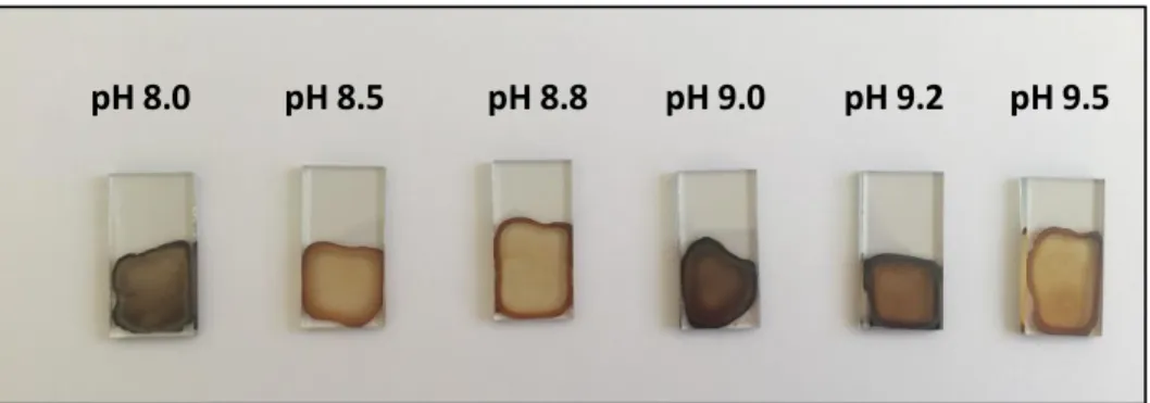
Figure II - 4: Aqueous dispersions of Mo thio, oxo-thio complexes 0.01M with pH range 8.0 < pH < 9.5 from the left to the right, S/Mo = 5. ... 113 Figure II - 5: Mo thio oxo-thio films with different pH deposited on FTO substrate and dried at 110°C, 10 min in Air. ...114 Figure II - 6: The light that encounters a material can be reflected, transmitted, or absorbed [5]. ... 119 Figure II - 7: Absorbance spectra of atomically thin layer at photon energy [8]. ...120 Figure II - 8: Tauc plots for (a) direct and (b) indirect bandgaps. Figures are adapted from [10]. ...121 Figure II - 9: Schema of the in plane electrical conductivity measurement using the four point probe technique [13]. ... 122 Figure II - 10: (a) and (b) photoelectrochemical cells in three-electrode configurations used for PEC and hydrogen measurements, (c) visible-light simulator... 124 Figure II - 11: Simplified Randles Cell Schematic Diagram. Source: Gamry Electrochemistry. 126 Figure II - 12: Nyquist Plot for a typical Simplified Randles cell. Source: Gamry Electrochemistry. ... 127 Figure II - 13: Sketch of the light signal focused on a surface during IMPS [19]. ...129 Figure II - 14: A calculated example of complex photocurrent or IMPS spectrum for a photoanode, illustrating the recombination (upper quadrant) and attenuation (lower quadrant) semicircles [20]. ... 130 Figure II - 15: Set-up of the IPCE measurements. LED is centered in front of the photocathode in the cell, where a diverging beam of ≈ 10mm is emitted towards the surface of the sample.. 132 Figure II - 16: Photoelectrochemical cell – gas chromatograph set up for hydrogen measurements... 133
Figure III - 1: SEM image of WSe2 electrodes in cross-section morphology...140
Figure III - 2: XRD patterns o f WSe2 (a) co mmercial po wder and (b) nanosheets films
o n FT O substrate after heat treatment at 350 °C in N2. ...141
Figure III - 3: Absorptance (black curve), transmittance (red curve) and reflectance (blue curve) of as-exfoliated WSe2 nanoflakes drop casted on glass substrate and annealed at 350°C under N2
atmosphere. The discontinuity observed on the experimental transmittance and absorbance curves probably arises from the switch from the Xe lamp used to ensure the whole range of wavelength investigated... 142 Figure III - 4: Absorbance curve extrapolated for the 2D WSe2 nanoflakes obtained using the
Beer-Lambert law, which considers the attenuation of the transmitted fraction of the light... 143 Figure III - 5: Mott-Schottky plot of exfoliated WSe2 showing a negative slope that corresponds
with p-type semi-conduction. Obtained at 0.5M H2SO4. ... 143
Figure III - 6: Linear scanning voltammetry curve of p-WSe2 electrode under constant chopped
illumination. Scan Rate 10mV s-1 in 0.1M Na
2SO4. ... 145
Figure III - 7: LSV curves (log |i| vs. Potential) under chopped light of WSe2 films displaying of
various thickness in 0.1M Na2SO4, annealed at 250°C under N2...146
Figure III - 8: j-E curve registered for 2D exfoliated WSe2 film after HTS treatment (5% w.t.) in
Figure III - 9: LSV curves recorded on WSe2 electrodes (a) after HTS treatment and Pt-Cu
deposition, (b) after Pt-Cu deposition without HTS treatment in 0.1M Na2SO4. ...149
Figure IV - 1: Typical ESI-MS spectra recorded on Mo thio complexes solution prepared at pH 9.00 and S/Mo=5. ... 157
Figure IV - 2: Peak identification of m/z=416.6, (Mo2S6O2H)-. Calculated isotope pattern of (Mo2S7H)- is given for comparison. The smaller mass difference value (1.93 mDa vs 16.46 mDa) is in agreement with attribution of this experimental peak to (Mo2S6O2H)- vs (Mo2S7H). ... 157
Figure IV - 3: Peak identification of m/z= 288.7, (Mo2S12)-2. ...158
Figure IV - 4: Peak identification (c) m/z= 280.7, (Mo3S8O)-2...158
Figure IV - 5: Peak identification of m/z= 274.8, (MoS5OH)-...159
Figure IV - 6: Species predominance diagram determined at 0.01 M Mo and S/Mo= 5 from ESI-MS data showing concentration peaks for (Mo2S12)2-, (Mo2S6O2)2- and (Mo3S8O)2- complexes between pH 8.0 and pH 9.7... 160
Figure IV - 7: XPS spectra of Mo thio complexes films prepared form solutions prepared at S/Mo= 5 and drop casted on FTO electrodes. Top: Mo 3d and S 2s region. MoS2 (blue line), MoO3 (green line), MoOySz (red line) S2- and (S2)2- (Yellow line). Down: S 2p region: terminal (S2)2- (red line), bridging (S2)2- (blue line), (SO4)2- (green line). ... 161
Figure IV - 8: XPS core-level spectra and deconvolution into S 2p (left column) and Mo 3d (right column) contributions for Mo thio complexes thin films deposited by (a)-(b) drop-casting onto FTO electrodes (c)-(d) drop casting onto WSe2 electrodes. XPS spectra were recorded after heat treatment 110 °C, Air 10 min, immersion in H2SO4 0.5 M. ... 163
Figure IV - 9: Optical Microscopy image of thio, oxo-thio Mo complexes film drop casted on FTO substrate showing a continuous phase and acicular precipitates. ... 163
Figure IV - 10: (a) Micro-Raman spectrum recorded on the continuous phase. (b) Micro-Raman spectrum recorded on the acicular particles. ...164
Figure IV - 11: Electrochemical and photo-electrochemical characteristics of catalysts films. MoxSy at S/Mo = 5, pH 8.8 on (a) FTO substrate and (b) drop casted on WSe2 photo-electrode; (c) (Mo2S12)2- on FTO substrate, (d) (Mo2S12)2- drop casted on WSe2 photo-electrode. ... 166
Figure IV - 12: Electrochemical characterization of MoxSy complexes films prepared at S/Mo= 5 and at various pH synthesis in H2SO4 0.5 M. (First row) J-E curves under intermittent illumination of corresponding films prepared on FTO are given as control. (Second row) The J-E curves are recorded under intermittent illumination on films prepared by drop casting onto WSe2 electrodes. ...167
Figure IV - 13: J-V curves recorded in 0.5 M H2SO4 on WSe2 electrodes after selective dip coating into Mo complexes-solutions at various S/Mo = 5 and various pH range. The blue curves represent the photocurrent of bare 2D WSe2 photo-electrode. ... 169
Figure IV - 14: J-V curves recorded in 0.5 M H2SO4 on WSe2 electrodes coated by (a) Mo thio complexes (S/Mo= 5, pH 8.8) film deposited by drop casting (b) pure (Mo2S12)2- complex film deposited by drop casting (c) Mo thio complexes (S/Mo = 5, pH 9.0) film deposited by selective dip coating. Films were calcined 110 °C, 10 min under Air atmosphere before photo -electrochemical testing. ... 169
Figure IV - 15: LSV curves recorded on films dip coated (a) 2h, (b) 8h and (c) 2x 16 h showing increase of photocurrent intensity with dip coating duration times. Electrolyte: H2SO4 0.5 M.
...170 Figure IV - 16: XPS spectra recorded on (a) Mo thio complexes films prepared by drop casting on FTO electrodes are given for comparison. Mo thio complexes films dip coated (b) 4h and (c) 2x 16h after photo-electrochemical testing in 0.5 M H2SO4. Mo 3d and S 2s region: MoS2 (blue
line), MoO3 (green line), MoOySz (red line), S2- and S22-, (Yellow line). S 2p and Se 3p region:
terminal S22- (red line), bridging S22- (blue line), SO42- (green line) Se 3p (green line). ...171
Figure IV - 17: LSV curves under intermittent (1 sun) illumination showing higher photocurrent on WSe2 photoelectrode after deposition of oxo-thio Mo complexes (S/Mo= 5. 2 x 16 h)
compared with HTS free-WSe2 photo- electrode activated by a Pt-Cu catalyst. ... 172
Figure IV - 18: LSV curves of WSe2 dip coated 2x16h on Mo complexes catalysts at different pH
and S/Mo ratio = 5. Electrolyte: 0.5 M H2SO4. Insert: Zoom of the low over-potential region
highlighting electrocatalytic performances of the various Mo thio complexes catalysts. ... 173 Figure IV - 19: Chrono-amperiometric curve recorded on WSe2 electrodes activated by Mo
oxo-thio complexes (2x 16h) in 0.5 M H2SO4 under intermittent illumination (100 mW cm-2). ... 174
Figure IV - 20: H2 GC peak areas determined on a Pt electrode (calibration cell) and on WSe2
photo-electrode activated by MoxSy complexes catalyst. Electrolyte: 0.5 M H2SO4. Counter
electrode: Pt. 1 Sun illumination. ... 174 Figure IV - 21: HRTEM images of the (a) ultrathin amorphous film of catalyst with thickness varying from 2 to 8 nm, (b) crystallized 2D WSe2 nanoflakes of ≈ 12 nm thickness and the
ultrathin catalyst film. ... 175 Figure IV - 22: XPS core-level spectra and deconvolution into (a) S 2p and (b) Mo 3d contributions for Mo thio complexes thin films deposited by selective dip coating onto WSe2
electrodes. Recorded after heat treatment 110 °C, Air 10 min, immersion in H2SO4 0.5 M, 15 min.
... 177 Figure IV - 23: Raman spectra of Mo thio complexes films fabricated from solutions at S/Mo= 5 and at various pH and deposited by (a) drop casting onto FTO and (b) dip coating on WSe2
electrodes. Raman spectra were recorded after heat treatment 110 °C, Air 10 min, immersion in 0.5 M H2SO4. For the selective dip coated film onto WSe2 electrodes, spectra were recorded after
electrochemical testing. ...178 Figure IV - 24: transmission, reflectance and absorption curves of co catalyst films drop casted on FTO from thio-, oxo-thio-Mo complexes solutions (S/Mo= 5, pH 9.0). The co-catalyst films were Air evaporated at room temperature and heat treated at 110°C under air...179 Figure IV - 25: (a) Tauc’s Plot obtained from UV-vis absorption data recorded on MoxSy complex
co catalyst film drop casted on FTO substrate. (b) Mott-Schottky plot of Mo complexes co catalyst – FTO showing a positive slope and a flat band potential EFb= +0.47 V vs NHE. ...179
Figure IV - 26: Band energy diagram of WSe2-Mo thio, oxo-thio catalyst photoelectrode. .... 180
Figure IV - 27: LSV curves under intermittent illumination (1.5 AM 100 mW cm-2) showing a
significant decrease of transient photocurrent on thio, oxo -thio Mo complexes coated WSe2
photo-electrode compared with a bare photo-electrode... 181 Figure IV - 28: Bode plots representation from EIS measurements of (a) bare and (b) Mo complexes co catalyst coated WSe2 photo electrodes under illumination (λ = 450 nm) at various
Figure IV - 29: Association Zarc elements in series to account for the different time constants.
Zarc is equal to CPE but make extraction of capacitance straightforward. ...182
Figure IV - 30: Admittance representation from EIS measurements of (a) bare and (b) Mo complexes co catalyst coated WSe2 photo electrodes under illumination (λ = 450 nm) at various
applied potentials from 0.2 V to -0.15V vs NHE. Electrolyte 0.5 M H2SO4, pH1. ... 183 Figure IV - 31: (a) variation of the interfacial capacitance, (b) variation of the different resistances extracted from fit parameters for bare WSe2 and coated WSe2 at different polarization
potentials...184 Figure IV - 32: Photoluminescence spectra of bare WSe2 (red curve) and WSe2 with Mo thio
complexes (black curve) catalyst film photo-electrodes. ...185 Figure IV - 33: Atomic structure and densities of state for a) Se-vacancy and b) W-vacancy in a (7x7) supercell... 186 Figure IV - 34: (a) Side views and (b) top views of the atomic structures for the Mo oxo -thio complexes on WSe2 monolayer possessing a W-vacancy, showing S-Se interactions and
accessible disulfide groups for the dimer Mo complexes. From left to right: adsorption of MoS4,
MoS3O, Mo2S12 and Mo2S6O2 radicals. Yellow: Sulfur, Red: Oxygen, Violet: Mo, Green: Se and
Grey: W. ...187 Figure IV - 35: Atomic structures of the thio and oxo-thio complexes from left to right: MoS3O,
Mo2S12 and Mo2S6O2 on a) free-defect pristine and b) Se-vacancy WSe2 monolayer. The smallest
distances between the Mo-cluster and the substrate are also given... 188 Figure IV - 36: Free energy diagram for Hydrogen evolution at equilibrium. (a) ΔGadsH showing
values close to the optimum of the volcano curve for free standing (Mo2S12)2- and (Mo2S6O2)
2-complexes (b) ΔGadsH values for WSe2 monolayers alone, namely point defect –free or W or Se
vacancies-containing WSe2 monolayers (c) ΔGadsH values for various adsorbed Mo complexes
on point defect –free or W or Se vacancies-containing WSe2 monolayers. ... 189
Figure V - 1: Process route for the self-assembling of TMDC nanosheets. The self-assembly is driven by complexing interactions involving a chalcogenide oligomer ligand localized on the outer surface of the colloid template. ...200 Figure V - 2: 119Sn liquid NMR spectra recorded on Sn (IV)-Sb
2S3 concentrated colloidal
dispersions (200 g.l-1 , Sn(IV)
molar = 0.25 and 0.5 - green and red traces, respectively). 119Sn liquid
NMR spectrum (blue trace) recorded in similar conditions on the ultrafiltrate collected by ultrafiltration on a 3 KD membrane is given for control. ...201 Figure V - 3: Scheme of the self-assembly process to elaborate nanojunctions of rGO-WSe2 with
juxtaposed nanoflakes with high surface area... 202 Figure V - 4: TEM images of (a) GO nanosheets selected at 15 300 rp; (b) exfoliated WSe2
nanoflakes after selection at 800 rpm and (c) SnxSbySz colloids showing a monodisperse
repartition of individualized spheres. ... 202 Figure V - 5: Pore distribution of 3D assemblies prepared from various 2D nanosheets and using Sb2S3-SnS2 colloidal spherical templates and GO nanosheets. (a) Pore area characteristics of
nanostructured WSe2 flakes selected at 800 rpm; (b) Pore volume determined from N2
adsorption-desorption data; (c) smaller pore volumes and more polydispersity pore distributions were observed for assemblies prepared from GO nanosheets. ... 203
Figure V - 6: Focused ion beam-scanning electron microscopy images in cross-section of WSe2
films on FTO substrate: (a) 2D exfoliated photoelectrode of WSe2, (b) 3D rGO-WSe2
photoelectrode after self-assembly process. Insert: higher magnification of 3D rGO-WSe2
self-assemblies showing interconnected nanoflakes with anisotropic orientation. ... 205 Figure V - 7: TEM image detailing the arrangement of self-assembled 3D rGO-WSe2 nanoflakes
uniformly distributed in the nanostructure network...206 Figure V - 8: XRD patterns of WSe2 bulk (red line), exfoliated WSe2 (green line) and 3D
self-assembled WSe2 (blue line) photoelectrodes after calcination at 350°C/2h at N2 atmosphere.207
Figure V - 9: J-V data for the conductivity measurements on films of 2D WSe2, 3D
free-rGO/WSe2 and 3D rGO-WSe2 films drop casted on glass substrate, at 25°C...208
Figure V - 10: Scheme representing the morphology of the 3D rGO-WSe2 self-assemblies,
showing anisotropic morphology of WSe2 building blocks (blue objects) and rGO nanosheets
(grey objects) and continuity of the coating film on the FTO substrate...209 Figure V - 11: HRTEM top view images of 3D rGO-WSe2 nanoflakes and MoxSy complexes catalyst
in formation of a hetero-structure, showing (a) the arrangement of the TMDC nanosheets and the film constructed in the nanosheets periphery; (b) higher magnification of the WSe2
nanoflake showing no degradation after co-catalyst deposition...210 Figure V - 12: (a) ADF image of textured WSe2/RGO photoelectrode film in presence of Mo thio
oxo-thio complexes catalyst; (b) 3D elemental mapping reconstructed from the sample shown in (a). Colors indicate atomic species: red (C), dark green (O), green (W), blue (Se), purple (Mo), dark blue (S). ...211 Figure V - 13: (a) ADF image of 3D rGO-WSe2/MoxSy hetero-structure. (b) 3D elemental mapping
reconstructed from the sample shown in (a). Colors indicate atomic species: red (C), dark green (O), green (W) and blue (Se)... 212 Figure V - 14: XPS core-level spectra and deconvolution into W 4f contributions for (a) 3D rGO-WSe2/MoxSy hetero-structure and (b) 2D WSe2/MoxSy film. ... 213
Figure V - 15: XPS core-level spectra and deconvolution into C 1s contributions of exfoliated 3D rGO-WSe2/MoxSy... 214
Figure V - 16: XPS core-level spectra and deconvolution into (a) Mo 3d contributions for a dip coated 3D WSe2/RGO thin film. (b) S 2p spectra consist of two different doublets (S 2p1/2 and S 2
p3/2). ... 215
Figure V - 17: J-V photocurrent density-voltage curves recorded on exfoliated WSe2 2D (red
curve), 3D free rGO-WSe2 (red curve) and 3D rGO-WSe2 (blue curve) films. ... 217
Figure V - 18: (a) LSV curves of 3D rGO-WSe2 photoelectrodes with different rrGO ratios under
internment light (100 mW cm-2). Electrolyte: 0.5M H
2SO4...219
Figure V - 19: Nyquist plots of 3D rGO-WSe2 photoelectrodes with different rrGO ratios.
Electrolyte: 0.5M H2SO4. AC impedance measurements at -0.2 V vs NHE. ...219
Figure V - 20: Linear Scanning Voltammetry (LSV) curves recorded on 3D self-assembly of rGO-WSe2 nanoflakes (blue trace). Electrolyte: 0.5 M H2SO4. LSV curves recorded on bare WSe2
(black trace) and 2D WSe2/MoxSy film (red trace) are given for comparison. ... 222
Figure V - 21: LSV curves recorded on 3D self-assembly of WSe2 nanoflakes (green trace), 3D
rGO-WSe2 (orange trace), free-rGO 3D WSe2/MoxSy (cyan trace) and 3D rGO-WSe2/MoxSy (blue
trace). Electrolyte: 0.5 M H2SO4. Mo thio complexes aqueous solution (S/Mo= 5; pH 9.0)
Figure V - 22: Nyquist plots obtained from EIS data of (a) 2D WSe2 and (b) 3D rGO-WSe2 before
Mo thio, oxo-thio catalyst deposition. Electrolyte: 0.5M H2SO4. Potential range: from 0.2 to -0.2V
vs NHE; under illumination (λ = 450 nm). ... 224 Figure V - 23: Nyquist Plots obtained for (a) 2D WSe2-MoxSy and (b) 3D rGO-WSe2-MoxSy films
in 0.5M H2SO4. AC impedance measurements were carried out between 0.2 and -0.2 V vs NHE,
under illumination (λ = 450 nm). Electrolyte: 0.5M H2SO4. ... 224
Figure V - 24: Bode plots representation of phase angle variation from EIS data of (a) bare 2D WSe2, (b) bare 3D rGO-WSe2, coated (c) 2D WSe2 and (d) 3D rGO-WSe2 with MoxSy co-catalyst
photoelectrodes under illumination (λ = 450 nm) at various applied potentials from 0.2 V to -0.2V vs NHE. Electrolyte 0.5 M H2SO4. ... 225
Figure V - 25: Admittance representation from EIS data of (a) bare and (b) Mo complexes co catalyst coated 3D rGO-WSe2 photo electrodes under illumination (λ = 450 nm) at various
applied potentials from 0.2 V to -0.2V vs NHE. Electrolyte 0.5 M H2SO4. ... 226
Figure V - 26: (a) variation of the charge transfer resistances and (b) variation of the interfacial capacitance extracted from fit parameters for bare 3D rGO-WSe2 and coated 3D rGO-WSe2 at
different polarization potentials and under illumination (λ = 450 nm). ... 227 Figure V - 27: UV-vis absorption (red marks) and IPCE (black curve) spectra for the MoxSy coated
photoelectrode of 3D rGO-WSe2 are shown together. ... 229
Figure V - 28: Photoluminescence performed on bare 3D rGO-WSe2 at 300 K. ... 230
Figure V - 29: Photoluminescence performed on 3D rGO-WSe2/MoxSy films (a) at 300K and (b)
at 4K temperature. Peak attenuation is observed with the increase in laser power... 231 Figure V - 30: Representative IMPS data for (a) bare 3D rGO-WSe2 and (b) 3D rGO-MoxSy coated
with MoxSy catalyst under monochromic illumination (λ = 680 nm). Electrolyte: 0.5M H2SO4;
Potential range: from 0.2 to -0.1V vs NHE; Frequency range: 20k-0.1 Hz and AC amplitude: 0.1V. ... 232 Figure V - 31: Rate constants extracted from IMPS data for (a) bare 3D rGO-WSe2 and (b) 3D
rGO-WSe2 coated with MoxSy catalyst, at different applied potentials. Rate constants of
recombination are shown as black symbols; rate constants for surface charge transfer are shown as red symbols...233
Figure 1: Cumulative pore volume of different TMDC materials presented different nanoflakes thickness, determined from N2 adsorption-desorption data. WS2 - red curve (6000 rpm), WSe2 –
black curve (800 rpm). ... 243 Figure 2: (a) Absorptance (blue curve), transmittance (black curve) and reflectance (red curve) of as-exfoliated WS2 nanoflakes drop casted on glass substrate and annealed at 350°C under N2
atmosphere. (b) Absorbance spectra of WS2 thin film obtained using the Beer-Lambert law. 244
Figure 3: LSV curve obtained for exfoliated p-WS2 electrode deposited onto FTO substrate and
after annealing at 350°C, under N2 atmosphere. ... 245
Figure 4: LSV curve obtained in 0.5M H2SO4 for p-WS2 electrode after thio, oxo-thio catalyst
List of Tables
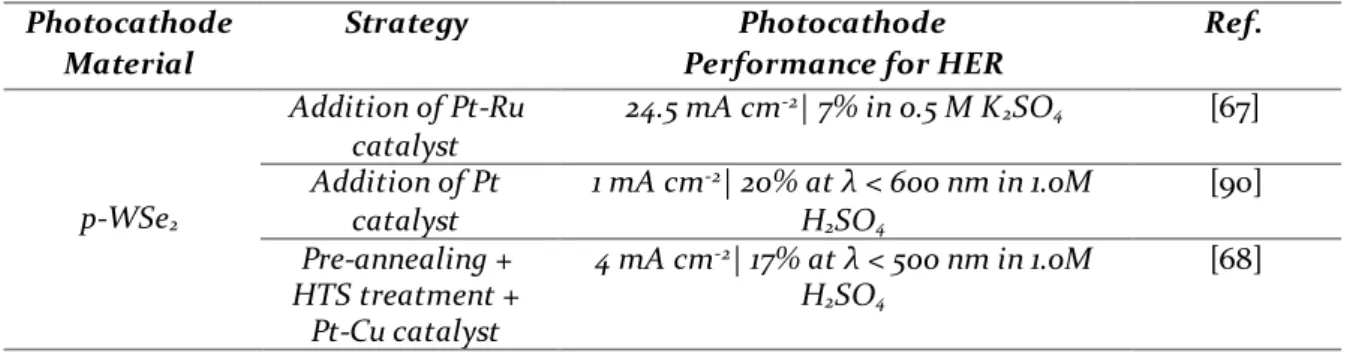
Table I - 1: summary of main requirements for solar water splitting...50 Table I - 2: p-WSe2 PEC performances previous reported in the literature for HER. ...85
Table III - 1: XRD data of bulk WSe2 used to calculate the size of ordered domains with the
Debye and Scherrer relation...141 Table IV - 1: Species concentration present at 0.01M Mo and S/Mo = 5 from ESI-MS data for different pH. ... 160 Table IV - 2: Mo concentration of catalyst loadings...165 Table IV - 3 : Adsorption energies (in eV) of various Mo-complexes in their radical forms, for three distinct substrate configurations of the WSe2 monolayer. ...187
Table V - 1: X-ray diffraction data, scattering angles and full width at half maximum intensities (FWHM) from Debye-Scherrer relation. ... 207 Table V - 2: rGO molar and mass ratios obtained from different volume of GO dispersions used for co-texturation with WSe2 nanoflakes...218
Introduction
The accelerated global warming and the world's high energy demand have led the scientific community to focus on the development of clean and renewable energy source [1]. Among the new alternatives, hydrogen is one of the most promising energy carriers. Its utilization as fuel is free of toxic gas formation and CO2 emission, where the only product is
water vapor [2]. However, hydrogen does not exist freely in nature and its production is still fossil-based [3]. With the global interest in solar energy research, clean hydrogen production can be accomplished making use of sustainable resources such as the sun and the water. For this purpose, semiconductor-based materials have been envisioned for solar energy harvesting, allowing for the conversion of photons to chemical compounds – hydrogen and/or oxygen – through charge separation [4], often denoted as solar-to-fuel conversion.
Among other possibilities, solar-to-fuel conversion can be achieved using a photoelectrochemical (PEC) device consisting of a semiconductor electrode in direct contact with a liquid electrolyte. The use of photoelectrochemical (PEC) for water splitting has received attention for being cost-competitive with fossil-based technologies in the techno-economic evaluation of hydrogen generation [5][6]. Indeed, for the realization of this hydrogen economy, the scientific community has been actively searching for efficient PEC cells composed of semiconductor photocatalysts earth-abundant and inexpensive [7].
Most of the studies are reported on n-type semiconductors [8]–[11], but the development of promising p-type semiconductor materials, exhibiting decent photocatalytic performances, were reported using photocathodes including p-type gallium indium phosphide (p-GaInP2),
p-type silicon (p-Si), p-p-type (p-Cu2O), such as CZTS (copper zinc tin sulfide, p-Cu2ZnSnS4) and
CIGS (copper indium gallium selenide, p-CuInGaSe2). However, their low stability and the
manufacturing high cost for large-scale still limit the use of these materials as photocathode devices [4]. To face this challenge, the development of new photocatalyst materials has been targeted to enable practical direct solar-to-hydrogen conversion, and so the realization of PEC involving low-cost, robust and high-performance semiconductor materials [5][7].
New opportunities have shown up with the emerging of 2D materials, displaying of unique optoelectronic properties and high specific surface areas that are important for catalysis and energy storage applications [12][13]. The layered structure of 2D materials favors maximum solar harvesting and decreases charge carrier pathways. Despite being graphene the most well- known layered material, transition metal di-chalcogenides (TMDC) also represents an interesting class of photoactive materials with the ability to be exfoliated into atomically thin 2D sheets. Their
structure and unique absorption properties provide tunable band-gap characteristics corresponding to the number of atomic layers [14] and strong light-matter interactions that offer outstanding performances in solar energy conversion [15]. Besides, viable routes for suitable economical production of large-area photocatalyst devices have been explored for further development of solar energy conversion procedures using these materials [15]–[17].
The 2D TMDCs have, however, a high concentration of surface defects that can act as efficient charge carrier traps (recombination sites) and are one of the most common scattering centers limiting the electron mobility [18]. The surfaces of the TMDCs have many electronic defects as unsaturated di-chalcogenides atoms on the edges. Previous works suggest that edges sites are detrimental to the photon-to-electron conversion efficiency, because the under-coordinated atoms on the edges are reactive toward surface corrosion processes and act as sites for charge carrier recombination [19].
Since the electrochemical reactions proceed at the electrode/electrolyte interface, at the semiconductor are generally complex, multistep and proton and electron transfer processes, which physically transpire on catalytic surface sites [4]. Therefore, rational control of the interface is required to adjust the semiconductor properties. As being one of the most important issues in photocatalysis [20], various strategies have been proposed to remove or neutralize these surface defects and thus, improve their performances in photocatalysis.
The main strategies involve surface treatments that include passivation of surface states, the addition of protection layers and co-catalysts – usually noble metals; and still p/n heterojunctions and doping [21]. For instance, HER was considerably improved on 2D WSe2
under visible irradiation with an optimized Pt-Cu co-catalyst combined with a defect passivation treatment [22]. Nevertheless, to make feasible a large-scale development of this technology, it is mandatory to replace the precious metal catalysts used with a more earth-abundant material. To perfectly suit the use in layered 2D materials, molecular co-catalysts can be very promising because they have ideal size matching, so they can easily be infiltrated into the layered structure and their thin films can minimize shielding [23]. MoS2-based nanomaterials were
previously proposed as earth-abundant alternative HER catalysts, such as the molecular Mo complexes including Mo3S4 [24], (Mo2S12)2-[25], (Mo3S13)2- [26]. Their promising catalytic
efficiency, comparable with the one of Pt [27], make them ideal candidates for use onto 2D photoactive materials such as the 2D TMDCs [28]. Also, as the defect sites found on the 2D TMDCs are very reactive [29], chemical bonding via ligand interactions at the surface of these
photocathodes could be seen as another interesting use of these molecular complexes to passivate surface defects.
Another important aspect is the morphology of the semiconductor and its nanostructuration. It is seen as an effective way to enhance the reaction kinetics thanks to both a more efficient charge transfer at the photoelectrode/electrolyte interface and a more efficient charge collection. Optical absorption is also supposed to benefit from a fine control of the photoelectrode material morphology [30]-[32]. However, morphology optimization techniques usually require heat treatments at high temperatures (> 400 °C) and these conditions are not suitable for many non-oxide semiconductors like chalcogenides or the processability into large-area of thin films [7]. Nevertheless, in a recent report [33] enhanced photoelectrochemical performance was achieved after a low-temperature nanostructuring technique for the obtention of mesoporous films exhibiting high surface area.
To some point, the high surface area can lead to poor effective charge mobility and the use of carbon-based nanojunctions, such as the graphene due to their metallic-like conductivity, is expected to allow for facile electron injection/collection within photoelectrode material [34]. Such kind of nanojunction has proven to lead to a superior photocatalytic activity for H2
evolution [35].
Among the challenges to fully take benefit of the layered morphology of the 2D materials, optimization of both the film microstructure and the charge collection towards the electrodes are highly desirable to significantly increase the access to catalytic sites, since packing of TMDC layers can occur with substantial restacking [36]. A relevant strategy may involve the design and fabrication of layered hetero-structures composed of interconnected nanoporous TMDC with high specific surface area, combined with carbon-based nanojunctions. In this context, the transition metal di-chalcogenides are promising candidates because of their good light absorption properties and are highly tunable: their number of layers can be tweaked to modify noticeably their properties.
Motivated by these reasons, the present work will be dedicated to the use of a 2D TMDC materials as photocatalyst for the hydrogen generation through solar water splitting and the application of potential strategies to improve its photocatalytic properties.
This thesis manuscript is divided into six chapters summing up all the important information and results that allowed for the accomplishment of this research work for 4 years.
The first chapter is focused on the presentation and contextualization of essential information about the hydrogen generation through solar water splitting. Basic notions of
semiconductors and their use in photocatalysis will also be discussed. Then, after a brief presentation of the suitable photoelectrode materials, this chapter will be dedicated to the use of 2D TMDC materials as photocatalysts, presenting their properties, their synthesis methods, based on what has been previously reported in the literature. After presenting the main bottlenecks of such materials, it will be present the strategies used in this work to achieve higher conversion efficiencies.
The second chapter will be devoted to the experimental methods used and developed all along this work: the semiconductor and co-catalyst synthesis, the electrode fabrication, the surface treatments, the thin film characterizations, the photoelectrochemical analyses and hydrogen measurements.
The third chapter will be focused on the exfoliated 2D p-WSe2 photoelectrode
characterizations achieved obtained via a simple synthesis route: such as optoelectronic characterizations and photoelectrochemical assessment. A comparison will be done after the electrodeposition of Pt co-catalyst together with the surface passivation, both inspired from previous works.
The fourth chapter will be dedicated to the development of cost-effective surface treatment of the exfoliated 2D p-WSe2. Water-stable Mo thio complexes as molecular
co-catalysts anchored onto the WSe2 photoelectrode via a solvent-free film-forming process will be
presented here. A proper complex selection upon deposition allows achieving both a defect healing and more efficient charge transfer, leading to improve significantly the photocatalytic performance of the p-WSe2 photoelectrode. Besides, these results will be supported by density
functional theory calculations that provide further insights into the interactions developed between the surface defects of the 2D photocathode and the Mo thio complex film catalyst, as well as the thermodynamics of H+ adsorption and H
2 desorption on the thio, oxo-thio complexes.
Within the fifth chapter is addressed the design and elaboration of nanostructured WSe2
photoelectrode with optimized morphology and conductivity property. It will be detailed the obtention of a 3D nanoporous network made of TMDC building blocks using a colloidal self-assembling process involving a post-etchable template and graphene oxide nanosheets. The experimental results will show that this nanostructuration procedure shows no chemical degradation of the TMDC materials while improving the photocatalytic performance, which is assured after deposition of MoxSy co-catalyst thin film. Further insights will demonstrate that
this approach leads to the elaboration of a photocathode with faster charge carrier collection and transfer as well as good results of incident photon-to-current conversion efficiency.
Finally, a last chapter in outlook will redirect the application of nanostructuring using the same colloidal self-assembly procedure, and defect passivation treatment with the use of thio, oxo-thio complexes catalysts for another TMDC material, the p-WS2. The preliminary results
will show that the approaches developed in this work are suitable for other 2D photocathode. Lastly, the perspectives for further development and evolution of this class of materials as photocatalyst for the construction of a photoelectrochemical system to afford efficient and economical conversion of solar energy into chemical fuel are highlighted.
BIBLIOGRAPHIC REFERENCES
[1] N. Z. Muradov and T. N. Veziroǧlu, “‘Green’ path from fossil-based to hydrogen economy: An overview of carbon-neutral technologies,” Int. J. Hydrogen Energy, vol. 33, no. 23, pp. 6804–6839, 2008.
[2] S. E. Hosseini and M. A. Wahid, “Hydrogen production from renewable and sustainable energy resources: Promising green energy carrier for clean development,” Renew. Sustain. Energy Rev., vol. 57, pp. 850–866, 2016.
[3] N. Armaroli and V. Balzani, “The hydrogen issue,” ChemSusChem, vol. 4, no. 1, pp. 21–36, 2011.
[4] K. Sivula and R. van de Krol, “Semiconducting materials for photoelectrochemical energy conversion,” Nat. Rev. Mater., vol. 1, pp. 15010, 1–16, 2016.
[5] B. A. Pinaud et al., “Technical and economic feasibility of centralized facilities for solar hydrogen production via photocatalysis and photoelectrochemistry,” Energy Environ. Sci., vol. 6, no. 7, pp. 1983–2002, 2013.
[6] C. Ding, J. Shi, Z. Wang, and C. Li, “Photoelectrocatalytic Water Splitting: Significance of Cocatalysts, Electrolyte, and Interfaces,” ACS Catal., vol. 7, no. 1, 2017.
[7] K. Sivula, “Advancing materials and methods for photoelectrochemical energy conversion,” Chimia (Aarau)., vol. 71, no. 7–8, pp. 471–474, 2017.
[8] M. S. Prévot, N. Guijarro, and K. Sivula, “Enhancing the Performance of a Robust Sol-Gel-Processed p-Type Delafossite CuFeO2 Photocathode for Solar Water Reduction,” ChemSusChem, vol. 8, no. 8, pp. 1359–1367, 2015.
[9] C. Jiang, S. J. A. Moniz, A. Wang, T. Zhang, and J. Tang, “Photoelectrochemical devices for solar water splitting-materials and challenges,” Chem. Soc. Rev., vol. 46, no. 15, pp. 4645–4660, 2017.
[10] P. Luan and J. Zhang, “Stepping towards Solar Water Splitting: Recent Progress in Bismuth Vanadate Photoanodes,” ChemElectroChem, vol. 6, no. 13, pp. 3227–3243, 2019.
[11] K. Sivula, F. Le Formal, and M. Grätzel, “Solar water splitting: progress using hematite (α-Fe 2O3) photoelectrodes,” ChemSusChem, vol. 4, no. 4, pp. 432–449, 2011.
[12] J. N. Coleman et al., “Two-dimensional nanosheets produced by liquid exfoliation of layered materials,” Science (80-. )., vol. 331, no. 6017, pp. 568–571, 2011.
[13] Q. H. Wang, K. Kalantar-Zadeh, A. Kis, J. N. Coleman, and M. S. Strano, “Electronics and optoelectronics of two-dimensional transition metal dichalcogenides,” Nat. Nanotechnol., vol. 7, no. 11, pp. 699–712, 2012.
31 [14] K. F. Mak, C. Lee, J. Hone, J. Shan, and T. F. Heinz, “Atomically thin MoS2: A new direct-gap semiconductor,” Phys. Rev. Lett., vol. 105, no. 13, pp. 2–5, 2010.
[15] X. Yu, M. S. Prévot, N. Guijarro, and K. Sivula, “Self-assembled 2D WSe2 thin films for photoelectrochemical hydrogen production,” Nat. Commun., vol. 6, no. May, 2015.
[16] V. Nicolosi, M. Chhowalla, M. G. Kanatzidis, M. S. Strano, and J. N. Coleman, “Liquid exfoliation of layered materials,” Science (80-. )., vol. 340, no. 6139, pp. 72–75, 2013.
[17] Y. Li, Y. L. Li, B. Sa, and R. Ahuja, “Review of two-dimensional materials for photocatalytic water splitting from a theoretical perspective,” Catal. Sci. Technol., vol. 7, no. 3, pp. 545–559, 2017.
[18] W. Zhu et al., “Electronic transport and device prospects of monolayer molybdenum disulphide grown by chemical vapour deposition,” Nat. Commun., vol. 5, pp. 1–8, 2014.
[19] J. M. Velazquez et al., “A Scanning Probe Investigation of the Role of Surface Motifs in the Behavior of p-WSe 2 Photocathodes,” Energy Environ. Sci., vol. 9, pp. 164–175, 2015. [20] J. Lu et al., “Atomic healing of defects in transition metal dichalcogenides,” Nano Lett., vol. 15, no. 5, pp. 3524–3532, 2015.
[21] N. Guijarro, M. S. Prévot, and K. Sivula, “Surface modification of semiconductor photoelectrodes,” Phys. Chem. Chem. Phys., vol. 17, no. 24, pp. 15655–15674, 2015.
[22] M. Johnson and K. Sivula, “Defect Mitigation of Solution-Processed 2D WSe 2 Nano fl akes for Solar-to-Hydrogen Conversion,” 2018.
[23] C. G. Morales-Guio and X. Hu, “Amorphous molybdenum sulfides as hydrogen evolution catalysts,” Acc. Chem. Res., vol. 47, no. 8, pp. 2671–2681, 2014.
[24] Y. Hou et al., “Bioinspired molecular co-catalysts bonded to a silicon photocathode for solar hydrogen evolution,” Nat. Mater., vol. 10, no. 6, pp. 434–438, 2011.
[25] Z. Huang et al., “Dimeric [Mo2S12]2- Cluster: A Molecular Analogue of MoS2 Edges for Superior Hydrogen-Evolution Electrocatalysis,” Angew. Chemie - Int. Ed., vol. 54, no. 50, pp. 15181–15185, 2015.
[26] J. Kibsgaard, T. F. Jaramillo, and F. Besenbacher, “Building an appropriate active-site motif into a hydrogen-evolution catalyst with thiomolybdate [Mo3S13]2- clusters,” Nat. Chem., vol. 6, no. 3, pp. 248–253, 2014.
[27] T. F. Jaramillo, K. P. Jørgensen, J. Bonde, J. H. Nielsen, S. Horch, and I. Chorkendorff, “Identification of Active Edge Sites for Electrochemical H2 Evolution from MoS2 Nanocatalysts,” Science (80-. )., vol. 317, no. 5834, pp. 100–102, 2007.
[28] A. B. Laursen, S. Kegnæs, S. Dahl, and I. Chorkendorff, “Molybdenum sulfides— efficient and viable materials for electro - and photoelectrocatalytic hydrogen evolution,” Energy Environ. Sci., vol. 5, no. 2, p. 5577, 2012.
[29] S. S. Chou et al., “Ligand conjugation of chemically exfoliated MoS2,” J. Am. Chem. Soc., vol. 135, no. 12, pp. 4584–4587, 2013.
[30] Y. Liu, Y. X. Yu, and W. De Zhang, “MoS2/CdS heterojunction with high photoelectrochemical activity for H2 evolution under visible light: The role of MoS2,” J. Phys. Chem. C, vol. 117, no. 25, pp. 12949–12957, 2013.
[31] T. W. Kim and K.-S. K.-S. Choi, “Nanoporous BiVO4 Photoanodes with Dual-Layer Oxygen Evolution Catalysts for Solar Water Splitting,” Science (80-. )., vol. 343, no. 6174, pp. 990–994, 2014.
[32] K. Sivula et al., “Photoelectrochemical water splitting with mesoporous hematite prepared by a solution-based colloidal approach,” J. Am. Chem. Soc., vol. 132, no. 21, pp. 7436– 7444, 2010.
[33] N. Guijarro, M. S. Prévot, X. A. Jeanbourquin, X. Yu, and K. Sivula, “Autodecomposition Approach for the Low-Temperature Mesostructuring of Nanocrystal Semiconductor Electrodes,” Chem. Mater., vol. 27, no. 18, pp. 6337–6344, 2015.
[34] S. J. A. Moniz, S. A. Shevlin, D. J. Martin, Z.-X. Guo, and J. Tang, “Visible-light driven heterojunction photocatalysts for water splitting – a critical review,” Energy Environ. Sci., vol. 8, no. 3, pp. 731–759, 2015.
[35] Z. Liu, H. Zhao, N. Li, Y. Zhang, X. Zhang, and Y. D u, “Assembled 3D electrocatalysts for efficient hydrogen evolution: WSe 2 layers anchored on graphene sheets,”
Inorg. Chem. Front., vol. 3, no. 2, pp. 313–319, 2016.
[36] D. Gerchman and A. K. Alves, “Solution-processable exfoliation and suspension of atomically thin WSe2,” J. Colloid Interface Sci., vol. 468, pp. 247–252, 2016
A
SOLAR WATER SPLITTING FOR HYDROGEN EVOLUTION ... 35
A.1
Context... 35
B
P
RINCIPLES OFS
OLARW
ATERS
PLITTING... 37
B.1
Processes in the photocatalytic water splitting... 37
B.2
Solar-to-Chemical Using Semiconductors...38
B.2.1 Some fundamentals about semiconductors ... 38 B.2.2 The semiconductor – electrolyte interface...40 B.2.3 Light absorption properties of semiconductors ... 44B.3
Photoelectrochemical Cell... 46
B.3.1 PEC Cells Configurations ...46 B.3.2 Main requirements to perform solar water splitting ...50
B.4
Emerging p-type Semiconductors as Photocathodes ... 50
B.4.1 p-type Metal Oxides ...51 B.4.2 p-type Silicon ... 52 B.4.3 p-type Metal Chalcogenides... 52 B.4.4 p-type Phosphides ... 52 B.4.5 Carbon-based semiconductors ... 53
B.5
2D TMDCs as promising materials for Solar Water Splitting ...54
C
TWO-DIMENSIONAL TMDCS FOR HER EVOLUTION... 57
C.1
Crystalline Structure... 57
C.2
Synthesis routes: bulk to ultrathin films of TMDCs ...58
C.2.1 The mechanical exfoliation process ...59 C.2.2 The chemical-exfoliation process...59 C.2.3 The solvent-exfoliation process... 60C.3
Optoelectronic Properties of 2D TMDCs ...62
C.3.1 Band gap and visible light absorbance ... 62 C.3.2 Influence of the type of the elements and their size ...64
D
DESIGN OF HIGH PERFORMANCE PHOTOCATHODE FOR HER ... 66
D.1
Morphology optimization to obtain high surface area
photocathodes ... 68
D.2
Surface defects – Main Challenges of the 2D TMDC Materials... 71
D.2.1 Classification of surface defects in TMDCs ...71 D.2.2 Effects of the defects onto TMDC properties ... 73 D.2.3 Strategies for defect passivation – Applications to 2D TMDCs ... 73D.3
Nanojunctions formed by semiconductor-carbon self-assembly .... 80
D.3.1 Interest of building TMDC- carbon nanojunctions... 81 D.3.2 Previous works of TMDC-carbon based for HER ... 81
D.4
Previous works of TMDC materials for solar water splitting ... 84
D.4.1 TMDC employed as photocathodes for HER ...84 D.4.2 TMDC and MoxSy molecular mimics complexes as a co-catalyst for HER...87
S
UMMARY AND WORK STRATEGIES... 91
BIBLIOGRAPHIC REFERENCES………..94A Solar Water Splitting for Hydrogen Evolution
A.1 Context
The urgency in finding new alternative clean, renewable energy supplies has origin from the increasing global reliance on non-renewable, geopolitically sensitive sources of energy such as natural gas and coal, coupled with highly volatile crude oil prices. According to Moniz et al. [1], global primary energy consumption in 2013 was about 17 TW, and is predicted to at least double by 2050. In this post-fossil fuel era, our society will require routes to efficiently convert renewable energy into chemical feedstocks and fuels using abundant starting materials like CO2,
N2, and water. The efficient electrochemical reduction of these starting materials into CO,
CH3OH, NH3, and H2 can potentially form the basis for a sustainable chemical network supplying
the manufacturing, agriculture, and transportation industries [2].
Hydrogen-based energy systems have attracted extensive attention because of their environmentally clean nature. The chemical energy stored in the H-H bond easily released when it combines with oxygen, yields only water as a reaction product. Accordingly, a future energy infrastructure based on hydrogen has been perceived as an ideal long-term solution to energy-related environmental problems [3],[4]. Hydrogen production is still based on raw fossil materials and only 4% is produced through water electrolysis [5]. Because of the increasing interest of producing hydrogen driven by the current concern about global climate change, new alternatives have been developed to produce hydrogen from environmentally friendly energies sources. Photocatalytic water splitting using solar energy for hydrogen production has become a challenging and attractive subject to work on [6].
In the past two decades, solar energy utilization has been the subject of intense research, development, and deployment efforts have been accelerated [7]. Engineering artificial photosynthetic systems to afford the efficient and economical conversion of abundant solar energy into chemical fuel on a scale in accordance with global energy demand (tens of terawatts) is an important step towards the realization of a sustainable carbon-neutral society. Electricity produced from solar energy has advantages over wind power and hydropower, since the latter two need turbines with moving parts that are both noisy and require much maintenance. However, the major disadvantage of solar energy is its intermittent nature. That is, the amount of sunlight a location receives varies greatly depending on the geographical location, time of day, season, and even clouds [8].
![Figure I - 1: Schematic of the fundamental mechanisms of photocatalytic water splitting [15]](https://thumb-eu.123doks.com/thumbv2/123doknet/2150337.9230/37.892.273.627.662.934/figure-i-schematic-fundamental-mechanisms-photocatalytic-water-splitting.webp)
![Figure I - 7: Energy bands in a system of two semiconductors chosen to generate opposite photovoltages [21]](https://thumb-eu.123doks.com/thumbv2/123doknet/2150337.9230/44.892.191.701.193.404/figure-energy-bands-semiconductors-chosen-generate-opposite-photovoltages.webp)
![Figure I - 16: Three-dimensional schematic representation of a typical MX 2 structure, with the chalcogen atoms (X) in yellow and the metal atoms (M) in grey [69]](https://thumb-eu.123doks.com/thumbv2/123doknet/2150337.9230/57.892.279.616.659.931/figure-dimensional-schematic-representation-typical-structure-chalcogen-yellow.webp)