SHERBROOKE
Faculte de genie
Genie electrique et genie informatique
The RatCAP Front-End Electronics
Electronique Frontale Integree pour le RatCAP
Ph.D. Thesis
Speciality: Electrical Engineering
Jean-Frangois PRATTE
Jury: Rejean Fontaine
Roger Lecomte
Paul O'Connor
Yves Berube-Lauziere
Mohamad Sawan
Sherbrooke (Quebec) Canada June 2008
Published Heritage Branch 395 Wellington Street Ottawa ON K1A0N4 Canada Direction du Patrimoine de I'edition 395, rue Wellington Ottawa ON K1A0N4 Canada
Your file Votre reference ISBN: 978-0-494-42689-0 Our file Notre reference ISBN: 978-0-494-42689-0
NOTICE:
The author has granted a non-exclusive license allowing Library and Archives Canada to reproduce, publish, archive, preserve, conserve, communicate to the public by
telecommunication or on the Internet, loan, distribute and sell theses
worldwide, for commercial or non-commercial purposes, in microform, paper, electronic and/or any other formats.
AVIS:
L'auteur a accorde une licence non exclusive permettant a la Bibliotheque et Archives Canada de reproduire, publier, archiver,
sauvegarder, conserver, transmettre au public par telecommunication ou par I'lnternet, prefer, distribuer et vendre des theses partout dans le monde, a des fins commerciales ou autres, sur support microforme, papier, electronique et/ou autres formats.
The author retains copyright ownership and moral rights in this thesis. Neither the thesis nor substantial extracts from it may be printed or otherwise reproduced without the author's permission.
L'auteur conserve la propriete du droit d'auteur et des droits moraux qui protege cette these. Ni la these ni des extraits substantiels de celle-ci ne doivent etre imprimes ou autrement reproduits sans son autorisation.
In compliance with the Canadian Privacy Act some supporting forms may have been removed from this thesis.
While these forms may be included in the document page count,
their removal does not represent any loss of content from the thesis.
• * •
Canada
Conformement a la loi canadienne sur la protection de la vie privee, quelques formulaires secondaires ont ete enleves de cette these. Bien que ces formulaires aient inclus dans la pagination, il n'y aura aucun contenu manquant.
The Center for Translational Neuroimaging of the Brookhaven National Laboratory has been studying the phenomenon of addiction, which has a direct impact on millions of people worldwide. This requires the development of new radiotracers for imaging specific neurotransmitter systems in the brain, and the design and implementation of novel imag-ing devices to measure the neuroactivity of the brain. The RatCAP, or Rat Conscious Animal Positron Emission Tomography (PET), is a head-mounted miniature PET scanner for brain metabolism imaging of awake rats with minimal mobility restriction to enable correlation with the animal's behavior.
The RatCAP detector is based on LSO scintillator crystals and avalanche photodiode (APD) arrays. The design of the RatCAP imposed stringent requirements on the read-out electronics. First, due to its size and limited power budget, VLSI of the front-end electronics was mandatory. Second, due to the weak signal to noise ratio from the APD detectors, the analog front-end noise had to be minimized, within the power budget, to provide the best possible timing resolution. Finally, the number of interconnections with the data acquisition system had to be minimal in order to maximize the animal's mobility.
This thesis presents the design and implementation of the ASIC for the RatCAP. The final ASIC integrates 32 channels consisting of a charge sensitive preamplifier, programmable gain, a bipolar shaping amplifier, and timing and energy discriminators. A novel 32-to-l address and timing serial encoder is integrated on-chip to multiplex the acquired data through a single output. The ASIC was realized in 0.18 \im CMOS technology from TSMC, has a size of 3.3 mm x 4.5 mm, and power consumption of 117 mW. The ASIC is fully operational. Noise characterization led to a measured equivalent noise charge of 650 electrons rms with the APD biased at the input. A coincidence timing resolution of 6.7 ns FWHM was measured between two typical LSO-APD-ASIC modules using a 68Ge source
(threshold at 420 keV). An energy resolution of 18.7% FWHM at 511 keV was measured for a 68Ge source.
The ASIC and the technology developed for the RatCAP have opened the door to the realization of many other systems, such as a PET-MRI scanner, and led to the granting of three patents and the publication of numerous scientific presentations.
Le Centre de neuroimagerie translationnelle du Brookhaven National Laboratory s'inte-resse depuis plusieurs annees au phenomene de la dependance, qui touche des millions de personnes a travers le monde. Pour y arriver, le developpement de nouveaux radiotra-ceurs selectifs aux neurotransmetteurs d'interet et la conception de nouveaux dispositifs d'imagerie sont essentiels pour mesurer l'activite neurologique du cerveau. Le RatCAP, ou Rat Conscious Animal PET, est un scanner miniature et portable qui s'installe sur le crane d'un rat pour obtenir l'imagerie T E P du metabolisme du cerveau chez le rat non-anesthesie pour ainsi permettre la correlation avec le comportement de l'animal. Le RatCAP utilise des cristaux de LSO couples a une matrice de photodiodes a avalanche (PDA) comme detecteur. Le RatCAP comporte des defis de taille pour la realisation de l'electronique. Premierement, du a la taille et la consommation de puissance limitee, 1'inte-gration a tres grande echelle de l'electronique est essentielle. Deuxiemement, etant donne que les detecteurs a PDA ont un rapport signal sur bruit faible, l'electronique analogique frontale doit etre optimisee pour minimiser le bruit electronique et ainsi permettre d'obte-nir la meilleure resolution temporelle possible. Enfin, le nombre d'interconnections avec le systeme d'acquisition doit etre garde au minimum pour maximiser la mobilite de l'animal. Cette these presente la conception et Pintegration de l'electronique frontale pour le Rat-CAP. Le circuit final est compose de 32 canaux contenant un preamplificateur de charges, un gain programmable, un filtre bipolaire semi-gaussien ainsi que des discriminateurs de temps et d'energie. Un encodeur serie, qui multiplexe dans une sortie l'information tem-porelle et l'adresse du canal ou Pevenement a ete detecte, est aussi integre dans le circuit pour minimiser le nombre d'interconnections avec le systeme d'acquisition. Le circuit a ete realise dans une technologie CMOS de 0.18 /zm, mesure 3.3 x 4.5 mm2 et consomme 117
mW. Le circuit est completement operationnel. Un bruit electronique de 650 electrons rms a ete mesure pour la chaine analogique avec la photodiode a avalanche polarisee a Pentree du circuit. La resolution temporelle pour deux modules de detection en coincidence avec une source de 6 8Ge est de 6.7 ns FWHM (seuil a 420 keV). La resolution en energie est de
18.7% FWHM pour une source de 68Ge.
Le circuit integre et la technologie developpes pour le RatCAP ont ouvert la voie a la realisation de nombreux systemes, tel un scanner TEP-IRM, ainsi que l'obtention de trois brevets et la publication de plusieurs communications scientifiques.
I would like to thank my thesis directors Rejean Fontaine, Roger Lecomte and Paul O'Connor for their advice, patience, mentoring and support. I am grateful to Craig Woody, Paul Vaska, David Schlyer and Veljko Radeka for giving me the opportunity to work on the RatCAP project. I will always remember the day I met you all in San Diego in October 2001, which significantly influenced the course of my career, and took me to the Brookhaven National Laboratory.
I would like to thank the RatCAP group for collaborating to the realization of the ASIC. The friendly atmosphere and dynamism of the group made this endeavor a wonderful and enriching experience.
The realization of this project was made possible with the tremendous help, advice and hard work of many of my fellow colleagues at the Instrumentation Division. I have learned so many things from you, and I will be forever grateful. Special thanks to Graham C. Smith, Pavel Rehak, Sergio Rescia, Bo Yu, Kevin Wolniewicz, John Triolo, Don Pinelli, Jack Fried, Ron Angona and Howard Hansen. I would like to acknowledge Sachin Jun-narkar, Grzegorz Deptuch and Stefan Robert for their contribution to the realization of the ASICs.
I would like to thank my mother Helene, my sister Marie-Claude and my close friends for their moral support. A very special thank you to my beloved wife, Genevieve, who has been supporting me unconditionally in this endeavor. Genevieve, I would not have made it without you, thank you so much.
Thanks to Sean Stoll for correcting the spelling and grammar of my thesis.
This work was supported by grants from the Canadian Microelectronics Corporation (CMC) and studentship awards from the Institut des Materiaux et Systemes Intelligents (IMSI) of Sherbrooke. This work was also supported by the Office of Basic Sciences of the U.S. Department of Energy and has been authored by employees of Brookhaven Sci-ence Associates, LLC under Contract DE-AC02-98CH10886 with the U.S. Department of Energy.
1 Introduction 1
1.1 The History of P E T Instrumentation 1 1.1.1 1951: The First Positron Emission Tomograph 1
1.1.2 1962: Multiple Detector Positron Imaging 2 1.1.3 1973: Cylindrical Detector Arrays . • 4
1.1.4 1973-1976: The First Whole Body and Commercial P E T 5 1.1.5 1973-1978: The Introduction of the BGO Scintillator 6
1.1.6 1979-1981: Analog Optical Multiplexing 6
1.1.7 1976-1980: Synthesis of FDG 7 1.1.8 1984-1985: The Block Detector 7 1.1.9 1989-1992: The Discovery of LSO Scintillator 8
1.1.10 1996: The First Avalanche Photodiode based P E T System 8
1.2 Imaging the Awake Animal 10 1.2.1 Human Addiction Studies 10 1.2.2 The RatCAP: Rat Conscious Animal P E T 10
1.3 The Front-End Electronics for the RatCAP 11
2 P h y s i c s and I n s t r u m e n t a t i o n of P E T 13
2.1 Principle of Positron Emission Tomography 13
2.2 Detectors used in P E T 15 2.2.1 Scintillators 16 2.2.2 Photodetectors . . . 17
2.3 Figures of Merit of P E T Systems 22
2.3.1 Energy Resolution 22 2.3.2 Timing Resolution 24 2.3.3 Spatial Resolution 25
2.3.4 Sensitivity 26 2.3.5 Noise Equivalent Count Rate 27
2.4 Small Animal P E T Systems 28 2.4.1 The quad-HIDAC 28 2.4.2 The MicroPET Family 31
2.4.3 The YAP-PET 32 2.4.4 The NIH Atlas and GE Explorer Vista 33
2.4.5 The A-PET and Philips MOSAIC HP 34
2.4.6 The ClearPET 34 2.4.7 The M A D P E T I I 37 2.4.8 T h e L a b P E T 38 2.4.9 The RatCAP . . 40
3 D e s i g n and Performance of C M O S C S P for A P D - P E T 45
3.1 Introduction 47
3.2 Charge Sensitive Preamplifiers 48 3.2.1 Design 48 3.2.2 Noise Optimization 49 3.3 Experimental Results 51 3.3.1 Electronic Characterization 51 3.3.2 ENC Measurements 51 3.3.3 Timing Measurements 56 3.3.4 Energy Resolution 57 3.4 Discussion 60 3.4.1 Electronics 60
3.4.2 Equivalent Noise Charge 60 3.4.3 Timing Resolution 61 3.4.4 Energy Resolution 61 3.4.5 Charge Sensitive Preamplifiers for PET 62
3.5 Conclusions 62 3.6 Acknowledgements 62
4 Front-end Electronics for the RatCAP 65
4.1 Introduction 68 4.2 The RatCAP Front-End Electronics 68
4.2.1 The RatCAP System 68 4.2.2 The RatCAP ASIC 69 4.3 Experimental Results 75
4.3.1 ICFSHLNA Measurements 75 4.3.2 ICFSHB01 Measurements 76
4.4 Discussion 79 4.5 Conclusion 80
5 The RatCAP Front-End ASIC 81
5.1 Introduction 84 5.2 The RatCAP ASIC 84
5.2.1 Analog Front-End 87 5.2.2 Timing Resolution and Photon Noise Model 89
5.2.3 Energy and Zero-Crossing Discriminators 91 5.2.4 Timing and Address Serial Encoder 94
5.2.5 System Readout 94 5.3 Experimental Results 97
5.3.1 Equivalent Noise C h a r g e 97
5.3.2 Energy Resolution 98 5.3.3 Timing Jitter and Time Walk 99
5.3.4 Timing Resolution and Scintillator Photon Noise Model Validation 100
5.4 Conclusion 102 5.5 Acknowledgment , 102
6.1 The RatCAP Performance 105 6.1.1 Timing and Energy Resolution 105
6.1.2 Spatial Resolution 106
6.1.3 Sensitivity 106 6.1.4 NEC 106 6.1.5 Animal Studies 107
6.2 Dual-Modality PET and MRI Scanner 108
6.2.1 The BNL PET-MRI 108 6.2.2 The Future PET-MRI Systems 112
6.3 The BNL Wrist Scanner 112 6.4 The Coded Aperture Gamma-Ray Imager 114
7 Conclusion 117 BIBLIOGRAPHY 122
1.1 First clinical positron imaging device. Dr. Brownell (left) is shown with
the scanner (1953) [BROWNELL, 1999] 2
1.2 Hybrid Positron Scanner [BROWNELL, 1999] 3
1.3 PC-I, the Is* tomographic PET imaging device [BROWNELL, 1999] 3
1.4 Picture of the BNL "Head Shrinker" developed by Robertson. Courtesy of
Brookhaven National Laboratory. 4 1.5 Pictures of the PETT-II (left) and PETT-III (right) developed by the
Phelps and Hoffman team [NUTT, 2002] 5
1.6 Illustration of Burnham's concept on analog coding by optical multiplexing
[NUTT, 2002] 7
1.7 The first block detector [NUTT, 2002] 8
1.8 Picture of the Sherbrooke APD-BGO PET Scanner 9 1.9 The Sherbrooke BGO-APD detector module. Two BGO scintillators of 3
x 5 x 20 mm3 are coupled to APDs of 4.2 x 4.2 mm2 (active area of 3.2
x 3.2 mm2). The detector module outer dimension is 3.8 x 13.2 x 33 mm3. 9
2.1 Illustration of the positron-electron annihilation and emission of the two
511 keV photons [CHERRY, 2006] 14
2.2 Illustration of true, scattered and random coincidences 15 2.3 Cross section of a typical reach-through APD along with the electric field
profile [PERKINELMER, 2006] 19
2.4 Equivalent Noise Charge model 23 2.5 Illustration of parallax error. The uncertainty in the line of response of the
positron annihilation increases with radial distance from the center of the field of view. On the right, the use of shorter crystal reduces the parallax
error, at the cost of the system sensitivity. 25 2.6 Sherbrooke PET/CT phoswich detector. The CsI(Tl) is used in CT mode,
whereas the pulse shape analysis of the scintillation light from the LSO or GSO gives depth of interaction in PET mode, and increases the achievable spatial resolution without any trade-off in sensitivity or increased cost with
increases in the number of channels 26 2.7 Schematic of the quad-HIDAC [MISSIMER et al., 2004] 29
2.8 Diagram of the HID AC detector module [JEAVONS et al, 1999] 29
2.9 T h e principle of coded center-of-cluster r e a d o u t [JEAVONS et al., 1983]. . . 30
2.10 Photograph of the YAP-PET [LAROBINA et al., 2006] 32 2.11 Picture of the detector and the ClearPET module [ZIEMONS and ON
BE-HALF OF THE C L E A R P E T COLLABORATION, 2004] 35 2.12 Picture of the detector modules of an early version of the ClearPET [STREUN
et al., 2006] 36 2.13 Diagram of the detector arrangement and a picture of the MADPET-II
camera [SPANOUDAKI, 2008] 37
2.14 Picture of the LabPET front-end PCB where the four quad-detector
mod-ules and the custom 16 channel ASIC is shown [BERGERON et al, 2007]. . 39
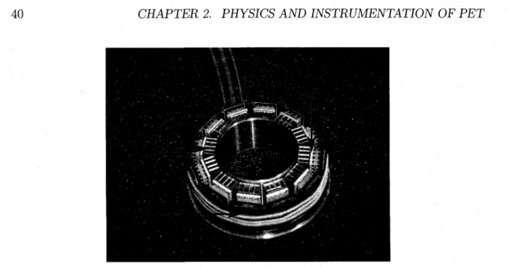
2.15 Picture of the LabPET module assembly. 39 2.16 Picture of the RatCAP camera without the cover. The LSO scintillator
array, APD and front-end ASIC are outlined 40
2.17 Picture of the LSO and APD arrays 41 2.18 Picture of the rigid-flex PCB for the RatCAP camera 41
2.19 Picture of the RatCAP camera 42 2.20 Photograph of a conscious rat in the RatCAP scanner during a PET scan,
including the support arm and data acquisition electronics (top) 43 3.1 CSP architecture. The transistor M2 is used as the main current source to
achieve the desired transconductance 49 3.2 Gain linearity for 1-mW CSP over operating range 52
3.3 Gain linearity for 5-mW CSP over operating range 52
3.4 ENC measurements for the 1-mW CSP 53 3.5 ENC measurements for the 5-mW CSP. The discontinuities are due to the
use of two different shapers (Ortec 579 Timing Filter Amplifier and the Ortec 673 Spectroscopy Amplifier) in order to cover a peaking time from
10 ns to 10 //s 54 3.6 ENC data fit with APD for the 1-mW CSP. A minimum ENC of 1117
electrons-rms at 100 ns was measured 54 3.7 ENC data fit with 10 pF for the 5-mW CSP 55 3.8 Electronic timing resolution for the 1-mW CSP. The Hamamatsu APD/LSO
detector was connected at the input and biased at a gain of 50 56 3.9 Electronic timing resolution for the 5-mW CSP. The Hamamatsu APD/LSO
detector was connected at the input and biased at a gain of 50 57
3.10 Timing resolution spectrum for the 1-mW CSP 58 3.11 Timing resolution spectrum for the 5-mW CSP. The time calibration was
obtained by adding an 8-ns delay to the stop channel 58 3.12 Energy spectrum for the 1-mW CSP connected to the Hamamatsu APD/LSO
detector biased at 380 V 59 3.13 Energy spectrum for the 5-mW CSP showing the electronic noise
contribu-tion measured with a pulser 59 4.1 Block diagram of the RatCAP front-end ASIC 70
4.2 CSP architecture 71 4.3 Analog front-end 71 4.4 Calculated and measured timing resolution of the analog front-end using a
Zero-Crossing Discriminator. A light output of 2300 photoelectrons and an
APD gain of 50 was used 74 4.5 Output of the serial encoder 75 4.6 ENC of the CSP connected to Hamamatsu APD (S8550) biased at 374 . 76
4.7 Linearity of the analog front-end for an input test capacitance of 12 pF. A gain of 15.2 mV/fC has been fitted in the designed operating region (up
to 130k electrons) 77 4.8 Energy resolution of the analog front-end connected to one channel of the
S8550 APD/LSO module for a 6 8Ge source. The energy resolution is 18.1%
FWHM 78 4.9 Electronic timing resolution of the analog front-end using the CFD as a
ZCD. A timing resolution of 3.54 ns FWHM was measured 78 4.10 Coincidence timing resolution of the analog front-end using the CFD as a
ZCD with APD/LSO detector. A timing resolution of 6.70 ns FWHM was
measured 79 5.1 Drawing of the RatCAP camera. Each detector block is composed of an
LSO crystal, APD and custom ASIC 85
5.2 Block diagram of a channel. 86 5.3 Microphotograph of the RatCAP ASIC. The 32 channel ASIC was realized
in TSMC 0.18 jum technology, has a size of 3.3 mm x 4.5 mm and has a
power consumption of 117 mW 88 5.4 Schematic of the comparator used to trigger on the zero-crossing of the
shaper's bipolar signal. It is implemented using a differential amplifier in open-loop. To prevent noise triggers, the transistor M17 is used to enable the comparator only when the amplitude of the shaper's signal is greater
than the low energy threshold 93 5.5 Block diagram of the chip encoder. Each of the 32 channels are connected
to a 32 input Wired-NOR, where the detected time of arrival of an event triggers the Control Signal Generator (CSG). The CSG will transmit the timing edge, asynchronously with respect to the 100 MHz system clock, through the single ASIC output. Each channel is also tied to a 32 to 5 priority encoder which generates the address of the channel that fired. The
address is then serialized through the same output as the timing edge. . . . 95 5.6 Oscilloscope capture of the pulse generator trigger used to inject the charge
in the ASIC (top), along with the shaper's bipolar signal (middle) and the encoder's digital output (bottom). The leading edge of the encoder's digital output represents the time of occurrence of a detected event, which
is followed by the 5-bit address of the channel that fired 96 5.7 Picture of the readout rigid-flex PCB of the RatCAP P E T camera before
being cut from the panel 96 5.8 ENC as a function of input capacitance. The marker represents the
mea-sured ENC of 650 e-rms with the APD biased at a gain of 45 98 5.9 Energy spectra of an LSO-APD-ASIC detector module using a 6 8Ge source.
An energy resolution of 18.7% (AE = 95.5 keV) FWHM is measured. . . . 99 5.10 Electronic timing jitter at the encoder's output. The error bars represent
the rms deviation of all the channels measured. Also plotted, the minimum
5.11 Coincidence timing resolution between two APD-LSO-ASIC detector
mod-ules. Energy threshold was set at 420 keV 102 6.1 Dopamine D2 receptor blocking study with 11C-raclopride. Images of
stri-ata from the same fully awake rat, before (top) and after (bottom) injection of blocking dose of unlabeled raclopride, summed over 60 minutes scan and
scaled to the same % injected dose per cc. (Rat weight is 280 gr.) 107 6.2 Simultaneous PET-MRI images of a rat injected with FDG in the Varian
human 4T MRI scanner. (MRI specifications: proton density, spin-echo TE/TR= 0.017/2 seconds. PET specification: 0.6 mCi of FDG, acquisition
time 68 minutes. Rat weight is 300 gr.) 109 6.3 Simultaneous PET-MRI image of rat striatum phantom using a surface coil
in the Bruker 9.4T 110 6.4 The RF quadrature saddle input coil designed to be inserted in the RatCAP
for dual-modality imaging in the Bruker 9.4T MRI . . . I l l 6.5 The RatCAP shielded enclosure for dual-modality imaging in the Bruker
9.4T MRI. The cuts in the copper were added to minimize eddy current
loops in the shielding I l l 6.6 Picture of the Aurora breast MRI scanner, (source: www.auroramri.com
/mri/index.shtml) 112 6.7 Drawing of the Aurora breast RF coil and the proposed PET add-on. . . . 113
6.8 Illustration of the 8 block Wrist Scanner 113 6.9 A coincidence planar image of the wrist phantom. Right: Anatomical view
of the human wrist pointing out the equivalent region of interest being
imaged (source: www.human-anatomy.net) ' 114 6.10 Pictures of the coded aperture GSO-APD based gamma ray imager without
2.1 Properties of Common Scintillators used in PET 17 3.1 LSO/APD Detector module specifications 48
3.2 Shaping form factors 50 3.3 Extracted noise parameters 55 3.4 Front-end for PET imaging 62 4.1 RatCAP CSP Characteristics 72 4.2 Values of passive components of the analog front-end 73
4.3 Comparison of the measured peaking time versus simulations 76 5.1 Measured characteristics of the two channels used in the timing resolution
model. The number of photoelectrons, APD gain and equivalent noise
charge are presented 100 5.2 Comparison of the model with the measurements of the timing resolution
for the two channels under test. The total timing resolution, along with the contribution from the electronic noise and photon noise are presented.
(All results in ns rms) 101
A c r o n y m Definition
APD Avalanche Photodiode
ASIC Application Specific Integrated Circuit BNL Brookhaven National Laboratory CFD Constant Fraction Discriminator
CMOS Complementary Metal Oxide Semiconductor CSG Control Signal Generator
CSP Charge Sensitive Preamplifier CT Computed Tomography DAC Digital to Analog Converter DAQ Data Acquisition System DOI Depth Of Interaction ENC Equivalent Noise Charge FOV Field Of View
FWHM Full Width at Half Maximum GSO Gadolinium Oxyorthosilicate LED Leading Edge Discriminator LOR Line Of Response
LSO Lutetium Oxyorthosilicate
LVDS Low-Voltage Differential Signaling
MOSFET Metal-Oxide-Semiconductor Field-Effect Transistor MRI Magnetic Resonance Imaging
NEC Noise Equivalent Count rate NIM Nuclear Instrumentation Module PCB Printed Circuit Board
PDA Photodiode a Avalanche PDE Photodetection Efficiency P E T Positron Emission Tomography P M T Photomultiplier Tube
QE Quantum Efficiency
RatCAP Rat Conscious Animal P E T RMS Root Mean Square
TDC Time to Digital Converter
TSMC Taiwan Semiconductor Manufacturing Company VLSI Very Large Scale Integration
ZCD Zero-Crossing Discriminator
Introduction
1.1 T h e History of Positron Emission Tomography
In-strumentation
The evolution of instrumentation for Positron Emission Tomography (PET) always had the objective of improving the achievable spatial resolution and sensitivity. Of course, the advance in PET was also intimately coupled to advances in radiopharmaceutical technol-ogy and image reconstruction algorithms, without which those sophisticated instruments are meaningless.
Although PET started in the 50's, it was not until the early 90's that it made its major transition from the research laboratories to clinical use. This is a rather slow evolution compared to computed tomography (CT) and magnetic resonance imaging (MRI) which moved quickly from early laboratory experiments to wide-spread clinical use. It was the precise detection of cancer lesions, not possible with other imaging modalities, and the assessment of the therapeutic treatment of cancer, which was awaited by a large population of patients, coupled with the availability of the proper radiopharmaceuticals for oncology that kicked off the use of PET in medical clinics.
In the following paragraphs, a review of PET instrumentation is presented. It is not intended to be a complete review of the contributions from all the world class scientists who dedicated their lives to the field, but to outline the major milestones in PET instru-mentation history, and have a better understanding of the state of the art systems cur-rently being realized. Other historical reviews can be found in [BROWNELL, 1999] [NUTT,
2002][MUEHLLEHNER and K A R P , 2006].
1.1.1 1951: T h e First Positron Emission Tomograph
The first use of annihilation radiation following positron emission for medical imaging is attributed to Gordon L. Brownell, director of the Physics Research Laboratory of the Massachusetts General Hospital (MGH), in collaboration with William Sweet, Chief of the Neurosurgical Service also from MGH. The system, built in 1951, consisted of two
Figure 1.1 First clinical positron imaging device. Dr. Brownell (left) is shown with the scanner (1953) [BROWNELL, 1999].
opposing 1 1/4" x 1 1/4" x 1 1/2" sodium iodide (Nal) crystals coupled to RCA 6199 flat-face photomultiplier tubes. The electronics consisted of tube amplifiers and cold-cathode glow tubes as counters. It was used for imaging patients with suspected brain tumors. They called those tests "positrocephalograms". This was the first clinical positron imaging device and is presented in Fig. 1.1. Those studies led to the first publication on positron imaging [SWEET, 1951]. The system contained several features that were incorporated into future positron imaging devices. For instance, data were obtained by translation of two opposed detectors using coincidence detection with mechanical motion in two dimensions. In the same year, Wrenn, Good and Handler (former President of the American Academy of Science), published an independent study on annihilation radiation detection [WRENN J R . et al., 1951].
1.1.2 1962: Multiple Detector Positron Imaging
The need for increased sensitivity pushed Brownell and his team to develop the first multiple detector positron imaging device in 1962 [BROWNELL et al., 1968]. The system consisted of two rows of nine detectors, each in coincidence with three detectors in the opposite row. The system could translate in one direction so that a two dimensional
Figure 1.2 Hybrid Positron Scanner [BROWNELL, 1999].
Figure 1.3 PC-I, the 1st tomographic PET imaging device [BROWNELL, 1999].
image could be acquired. It is shown in Fig. 1.2. This system was also designed for brain imaging and served as a clinical scanner at MGH for over a decade.
The next milestone in the evolution of PET, was the implementation of a camera with a two dimensional detector array (see Fig. 1.3). The camera, named PC-I, was also developed by Brownell's group between 1968 and 1971 [BURNHAM and BROWNELL, 1972]. But the most important contribution of the PC-I to the PET field was in the introduction of filtered back projection for image reconstruction [CHESLER, 1973]. From those data, David Chesler was able to produce three types of computed tomographic images: an emission image, a transmission image and an absorption-corrected emission image.
Figure 1.4 Picture of the BNL "Head Shrinker" developed by Robertson. Courtesy of Brookhaven National Laboratory.
1.1.3 1973: Cylindrical Detector Arrays
The next logical step in PET instrumentation was the development of circular or cylindri-cal arrays of detectors, which was first proposed by James Robertson [ROBERTSON et al., 1973], from the Medical Department of Brookhaven National Laboratory, and Z.H. Cho. The apparatus, known as the BNL "head shrinker", was realized by Robertson in col-laboration with Sy Rankowitz, William Higinbotham and Martin Rosenblum of the BNL Instrumentation Division. The system consisted of 32 detectors, first configured spheri-cally, then in a single plane, with the even ones inserted radially and the odd ones axially, as presented in Fig. 1.4. Each detector was made of a 1" Nal crystal and a PMT. Unfortu-nately, due to limited sampling, lack of attenuation correction and lack of a proper image reconstruction algorithm, they were unable to obtain true reconstructed cross sectional images. The system was then transferred to McGill's Montreal Neurological Institute. Proper image reconstruction were developed by Chris Thompson from McGill, and the "head shrinker" was modified to allow the patient to be scanned supine instead of seated
(a) PETT-II (b) PETT-III
Figure 1.5 Pictures of the PETT-II (left) and PETT-III (right) developed by the Phelps and Hoffman team [NUTT, 2002].
1.1.4 1973-1976: The First Whole Body and Commercial P E T
Concurrently, another group headed by Michel M. Ter-Pogossian and formed by Micheal Phelps, Ed Hoffman and Nizar Mullani at Washington University in St. Louis, along with James Kelly Milam, Charles W. Williams, Terry D. Douglass, and Ronald Nutt from EG&G ORTEC were also investigating PET instrumentation. Starting in 1973, a series of tomographs were built: the PETT-I, the PETT-II and the PETT-III (see Fig. 1.5). PETT stands for Positron Emission Transaxial Tomography. The PETT-II consisted of an hexagonal array of 24 Nal(Tl) detectors in coincidence, and made use of attenuation correction and a filtered back projection algorithm. All the electronics was NIM based. They started to build this system in December 1973, and the first data were acquired in January 1974. This scanner was used by the Phelps-Hoffman team to establish the math and physics of PET, and also to perform imaging of blood flow and metabolism in animals. The construction of the PETT-III started at the end of 1974. It was the first scanner intended for human PET. It consisted of 48 Nal(Tl) scintillators 5 cm in diameter and read out by PMTs, arranged in a hexagon. Sampling in this system was greatly improved by a combination of linear movement of the detector assembly and a 60 degree rotation of the gantry. A dedicated computer took care of the detector motion, gantry, bed, as well as image reconstruction and display. The realization of the PETT-III had a significant impact in the field of PET, as it lead to the first commercial PET scanner, the ECAT-II. This scanner, commercialized by EG&G ORTEC, had 96 3.75 cm diameter Nal(Tl) crystals. A PDP-11 computer with 32 kB of memory was used to control the scanner and reconstruct the images. The system was sold in 1978 for $600,000! The first
system was delivered to UCLA in 1976, which also coincided with Phelps and Hoffman moving from the University of Washington to UCLA.
1.1.5 1973-1978: T h e Introduction of the BGO Scintillator
Thus far, all the PET systems where using Nal(Tl) as a scintillator. But even though Nal(Tl) has high light output and a suitably fast decay time for coincidence detection, it is far from being ideal for PET. Its low density and effective atomic number limit the efficiency for 511 keV photon detection. Also, Nal(Tl) was difficult to use in dense arrays because of its hygroscopic nature. The quest for new scintillation materials for PET was ongoing, and the first alternative to Nal(Tl) was bismuth germanate (BGO). Weber at University of California, Berkeley, studied the luminescence of BGO in 1973 [WEBER and
MONCHAMP, 1973], and Nestor and Huang characterized the scintillation properties of BGO in 1975 [NESTOR and HUANG, 1975]. The first evaluation of BGO for PET was performed by Cho and Farukhi [CHO and FARUKHI, 1977] and Derenzo [DERENZO, 1981]. Their findings led to the first research PET scanner using BGO, which was developed by Chris Thompson and his group at the Montreal Neurological Institute in 1978. The same year, EG&G ORTEC produced the first commercial tomograph using BGO, the NeuroECAT.
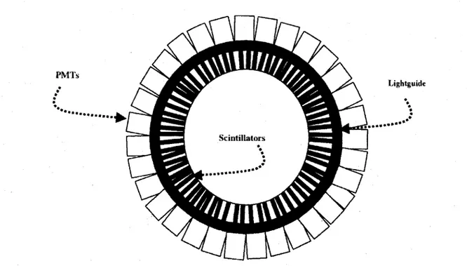
1.1.6 1979-1981: Analog Optical Multiplexing
While the 70's saw the birth of ring and cylindrical tomographs, one of the main drawback of these geometries was the limited sampling. Tricks such as wobbling the detector array were used to improve the sampling, but still, more needed to be done. The first step toward the solution is attributed to Stephen Derenzo from Berkeley, who built a cylindrical tomograph in which the Nal scintillators were closely packed to limit dead space, and individually coupled to a quartz "lightpipe" which would bring the light to the bulky PMTs further back [DERENZO et al., 1979]. But it was the work of Charles Burnham on analog coding by optical multiplexing which allowed the acquisition of high resolution PET images-without detector motion [BURNHAM et a l , 1981][BURNHAM et al., 1985]. Burnham's concept was to place individual small scintillators on a circular light guide with photomultipliers placed on the opposite side of the light guide, as illustrated in Fig. 1.6. Similar to the Anger Camera concept, by taking the ratio of 2 adjacent photomultiplier signals, the scintillator that detected the gamma ray could be identified.
PMTs
Figure 1.6 Illustration of Burnham's concept on analog coding by optical multiplexing
[NUTT, 2002].
1.1.7 1976-1980: Synthesis of FDG
Even though the evolution of radiopharmaceuticals is not covered in this historical review of PET instrumentation, it is worth mentioning that their development had a significant influence on the acceptance of positron imaging in clinical studies and the availability of funding for the realization of novel scanners . The radiopharmaceutical which had the biggest impact, and which is still the most widely used today, is 18F labeled
2-fluorodeoxy-D-glucose, known as FDG. FDG, which was developed by Al Wolf and Joanna Fowler's group at BNL [IDO et al., 1978], has a half-life perfectly suited for PET and allows precise values of energy metabolism in brain, heart and other organs.
1.1.8 1984-1985: T h e Block Detector
The optical multiplexing concept of Burnham presented in section 1.1.6 was using a con-tinuous light guide, causing the light generated by a scintillator to spread considerably. Consequently, a large number of PMTs triggered for a single 511 keV photon and in-creased the spatial extent of dead time. Moreover, the light guide was expensive, difficult to manufacture and limited the serviceability of the scanner. To address those issues, Mike Casey and Ronald Nutt, from CTI, introduced the "block detector" [CASEY and NUTT, 1986][CASEY et al., 1988], where multiple crystals were encoded to a single position
Lightguide
Figure 1.7 The first block detector [NUTT, 2002].
sensitive PMT. The first block detector had 4 PMTs with 8 BGO scintillators coupled to each of them, as seen in Fig. 1.7.
1.1.9 1989-1992: T h e Discovery of LSO Scintillator
Another major breakthrough in PET instrumentation was the discovery of Lutetium Oxy-orthosilicate (LSO) by Charles Melcher [MELCHER and SCHWEITZER, 1992]. Compared to BGO, which has 15% of the light output of Nal(Tl) and a decay time of 300 ns, LSO has 5 times more light output and a decay constant 7.5 times faster, leading to significitant improvements of PET scanner performance. The microPET, realized by Simon Cherry and his group at UCLA, was the first preclinical LSO PET tomograph [CHERRY et al., 1997].
1.1.10 1996: T h e First Avalanche Photodiode based P E T System
Finally, the latest major contribution to the advance of PET imaging was the use of the avalanche photodiode (APD) as photodetector, instead of the PMT [LIGHTSTONE
et al., 1986][CARRIER and LECOMTE, 1990]. APDs allowed for one to one coupling of
millimeter scale scintillators with the photodetector, with a granularity which cannot be achieved with PMTs. Moreover, compared to PMTs, APDs are insensitive to strong magnetic fields, which allows for dual-modality PET and MRI. The first PET scanner to use APDs was realized by Roger Lecomte's team at Universite de Sherbrooke in 1996
[LECOMTE et a l , 1996], and is shown in Fig. 1.8 along with a picture of the APD-BGO detector module in Fig. 1.9.
' • ^ ^ " ? m J* "wJ'V! ••'.'•-"•I
Figure 1.8 Picture of the Sherbrooke APD-BGO PET Scanner.
Figure 1.9 The Sherbrooke BGO-APD detector module. Two BGO scintillators of 3 x 5 x 20 mm3 are coupled to APDs of 4.2 x 4.2 mm2 (active area of 3.2 x 3.2 mm2). The
The history, and future, of PET instrumentation has been driven by the quest to improve spatial resolution and sensitivity. New detector development is accelerating the pace of positron imaging evolution, and every year new groups from around the world get into the race. In the last 10 years or so, dual-modality imaging devices, such as PET-CT, PET-MRI and PET-Optical tomography [KONECKY et al., 2008][CHERRY, 2006][PlCHLER et al., 2008][JUDENHOFER et al., 2008][CHERRY et a l , 2008], have improved and enhanced di-agnostic capabilities in clinical applications and opened new possibilities for research in preclinical applications by allowing registration of the metabolic information with precise anatomical reference points in the subject. Now, dedicated PET scanners for specific studies, such as breast imaging, are being designed. In the following section, the specific need for imaging the brain of awake small animals for behavioral and neurological studies will be presented.
1.2 I m a g i n g t h e Awake A n i m a l
1.2.1 Human Addiction Studies
Over the last 30 years, the Center for Translational Neuroimaging of the Brookhaven National Laboratory has focused its research on the integration of radiopharmaceutical chemistry with the tools of neuroscience to develop new scientific tools for applications in human health. One major area of research which has a direct impact on millions of people worldwide is the phenomenon of addiction and its implications in the neurochemistry of the brain. The scope of the research reaches from the understanding of drug and alcohol addiction, obesity and eating disorders, attention deficit hyperactivity disorder (ADHD), to the development of new strategies for addiction treatment.
The study of the phenomenon of addiction requires the development of new radiotracers for imaging specific neurotransmitter systems in the brain, and the design and realization of novel imaging devices to measure the neuroactivity of the brain.
1.2.2 The R a t C A P : Rat Conscious Animal P E T
Small animals, like rats, are used in medical research because they represent an excellent model of the human body and brain metabolism. Researchers from BNL proposed that the correlation of the animal's behavior with neurological study performed with PET imaging would allow unprecedented understanding of the addiction phenomenon. Hence, a PET camera allowing imaging of the awake rat was designed and realized, the RatCAP
(Rat Conscious Animal P E T ) . This is a major breakthrough in preclinical imaging of the brain as it allows imaging of small animals without the use of anesthesia which is currently required to prevent movement of the animal. Also, anesthesia produces profound effects on brain function, which biases any neurologic metabolism information obtained in standard P E T studies. With the RatCAP, the rat wears the camera, attached to its skull, eliminating the relative movement between the animal and the scanner.
1.3 T h e Front-End Electronics for the R a t C A P
This thesis presents the design and implementation of the front-end electronics for the RatCAP. By its nature, the RatCAP imposes unique challenges on the realization of the electronics. The objectives for the design and implementation of the RatCAP electronics are the following. First, due to the miniature size of the camera and the large number of readout channels, very large scale integration (VLSI) of the front-end electronics is mandatory. Second, in order to have minimal influence on the animal's behavior, the mobility of the camera has to be preserved as much as possible. Hence, the number of interconnections between the front-end electronics in the camera and the data acquisition system has to be minimized. Finally, the analog front-end has to be optimized for the detector characteristics, given a limited power budget of 1.5 W for the whole camera, to provide the best possible timing resolution. The power dissipation has to be limited to prevent the degradation of the detector's performance and influence the animal's behavior. The author of this thesis was the lead designer of the ASIC and was responsible for the implementation of the electronics in the RatCAP camera. His tasks included:
• Mathematical optimization of the timing resolution, through minimization of elec-tronics noise and optimization of the analog front-end according to the design spec-ifications.
• Design and implementation of the complete analog front-end, timing discriminator, energy discriminator, bias networks, LVDS receiver and transmitter.
• Design of the rigid-flex printed circuit board and support electronics.
• Close collaboration to the realization of the RatCAP system, more specifically on the detector and the data acquisition system.
This thesis consists of six chapters. In the next chapter, the principles of positron emission tomography along with the required instrumentation and the figures of merit of P E T will
be presented. Also, a review of state of the art preclinical small animal PET systems in the field will be covered. In the third chapter, the first peer reviewed paper on the charge sensitive preamplifiers design and evaluation of the TSMC CMOS 0.18 /xm technology are presented. Chapter 4 presents the second peer reviewed paper on the analog front-end electronics for the RatCAP. Chapter 5 presents the most recent paper on the complete application specific integrated circuit (ASIC) for the RatCAP. Finally, chapter 6 presents the performance of the RatCAP scanner and other systems which were realized based on the RatCAP technology and the ASIC.
Physics and Instrumentation of Positron
Emission Tomography
In the previous chapter, the evolution of P E T instrumentation was highlighted to put in context the technologies which are used now and the present thesis. The objective of this chapter is to present the concepts essential to understand positron emission tomography. In this line of thoughts, the physics of P E T is presented, along with P E T system perfor-mance figures of merit. The review of the main state of the art systems is also presented, with an emphasis on the front-end electronics architecture.
2.1 Principle of Positron Emission Tomography
Positron emission tomography imaging is based on two basic principles: imaging through the use of positron emission, also known as the tracer principle, and volumetric imag-ing of the body's interior, called tomography. The process of P E T imagimag-ing starts with the injection of a radiopharmaceutical into the subject. The purpose of the radiophar-maceutical is to selectively concentrate in the region of interest in the subject and emit positrons which are detected non-invasively and indirectly via the detection of gamma photons at 511 keV resulting from the annihilation of the positron and an electron (more details below). A radiopharmaceutical has two main constituents. The first component is a chemical compound which has the property, depending on the type of study which is performed, to selectively be metabolized by targeted cells or bind with receptors to be imaged. This leads to an increased concentration of positron emissions in the region of interest. The second component is the tracer. It is an unstable radioisotope synthesized in a cyclotron. The most probable deexcitation mode of the radioisotope's nucleus is through the conversion of a proton into a neutron, with the simultaneous emission of a positron and a neutrino. The positron travels in the tissue, loosing its kinetic energy principally through Coulomb interaction with electrons. As the rest mass of the positron is the same as that of the electron, the trajectory of the emitted positron deviates substantially with each Coulomb interaction. When the positron reaches thermal energy, it interacts with an electron, forming a hydrogen-like orbiting pair called positronium. The positronium is
Figure 2.1 Illustration of the positron-electron annihilation and emission of the two 511 keV photons [ C H E R R Y , 2006].
unstable and annihilates into a pair of anti-parallel 511 keV gamma photons, as illustrated in Fig. 2.1. The subsequent coincidence detection of the two 511 keV photons determines the line of response (LOR) where the annihilation of the positron-electron took place. It is the acquisition of all those LORs which allow the reconstruction of in vivo tomographic images.
It is important to outline at this point that the range of the positron, which depends on its energy and hence the radioisotope used, is one of the main physical processes which limit the achievable spatial resolution in preclinical small animal systems. To give an order of magnitude, nC and 1 8F in water will have 75% of their positrons annihilate within
2.1 mm and 1.2 mm of their origin respectively [WERNICK and AARSVOLD, 2004]. Also, due to the variation in the momentum of the positron, the two 511 keV photons will be noncolinear by approximately 4 mrad, which also limits the spatial resolution. The latter physical limitation is more important for clinical scanners than preclinical, as the error increases as a function of the diameter of the field of view. For example, a ring with a diameter of 60 cm will encounter a spatial resolution loss of 1.3 mm due to noncolinearity [ W E R N I C K and A A R S V O L D , 2004].
As previously presented, the coincidence detection of the two 511 keV photons determines the LOR of the annihilation. There are three types of detected coincidences, which are presented in Fig. 2.2. Scattered coincidence is defined as the detection of both annihilation photons originating from a single decay, but where one or both photons have lost some
I
I
t
Figure 2.2 Illustration of true, scattered and random coincidences.
energy by scattering in the subject. Random coincidence is defined as the detection of two 511 keV photons originating from two separate decays, but close enough in time to look like a single decay to the system electronics. Finally, true coincidence is the detection of both annihilation photons originating from the same nucleus decay where neither of the photons scattered in the subject.
True and scattered events are referred to as prompt coincidences as they originate from a single nucleus decay. Their detection rate increases proportionally to the activity of the radiopharmaceutical injected into the subject. The random events rate increases as the square of the activity and will dominate above a given activity level injected into the subject. For P E T imaging, it is desirable to measure and reconstruct true events, and discriminate scattered photons and random events. As it will be presented in section 2.3, the performance of the detector and front-end electronics have a direct impact on the amount of random and scattered coincidences accepted by the system.
2.2 Detectors used in P E T
The detector is a key element determining the performance of a P E T system. Hence it is important to understand how the different detectors use in P E T work and what are their characteristics.
The ideal detector would have the following properties. In order to increase the 511 keV photon's probability of having a photoelectric interaction and hence increasing the sen-sitivity of the system, it should have a high effective atomic number and high density. The ability of the system to discriminate scattered events accurately is function of the achievable detector energy resolution. It should provide the greatest amount of charge per
511 keV photon relative to the noise it generates. The electronics usually have negligible contribution to the system's energy resolution. In the same line of thoughts, the system's capability to discriminate random coincidences depends in great parts on the detector's time jitter contribution to the timing resolution. The narrower the time distribution of the collected charge from the detector by the front-end electronics, the smaller the detector's contribution to the timing resolution. Further details on energy resolution and timing resolution can be found in section 2.3. In order to allow high resolution imaging, the packing fraction of the detector should be high, to allow staggering of multiple detector elements with minimum dead space. Finally, if dual-modality P E T and MRI is desired, the detector operation should be immune to strong magnetic fields.
The detectors used in P E T are divided into two main categories. There are direct inter-action detectors, where the incident 511 keV photon ionizes the sensitive volume, creating free carriers which drift along the electric field applied between the electrodes. Examples of direct interaction detectors used in P E T are room temperature semi-conductors such as Cadmium Zinc Telluride (CZT), and multi-wire proportional chambers (MWPC). But the most common type of detectors used in P E T are known as indirect interaction detectors. These detectors consist of a scintillator coupled to a photodetector. The 511 keV photon interacts in the volume of the scintillator, which emits photons in the visible and near UV range. These photons will in turn create free carriers in the photodetector.
2.2.1 Scintillators
The two most probable mechanisms in which a photon in the energy range of 511 keV can interact in a scintillator are the photoelectric effect and Compton scatter effect [ K N O L L , 1999]. In the case of a photoelectric effect, the incident photon is absorbed by an atom of the scintillator, resulting in the ejection of an electron most likely from the K shell of the atom, called a photoelectron. The energy of the photoelectron is equal to the energy of the incident photon minus the binding energy of the ejected electron from its nucleus, which is in the range of a few tens of keV for typical scintillators used in P E T . The photoelectron passing through the scintillator's lattice will then create a large number of electron-hole pairs, where electrons are elevated to the conduction band. Due to some well selected impurities in the crystal, also called activators, possible energy states are created in the forbidden band of the scintillator's. The created holes will quickly drift to the activators site, ionizing them. Meanwhile, the electrons elevated to the conduction band will migrate in the lattice of the crystal until they encounter an ionized activator. The relaxation of an electron into a hole of the ionized activators will produce the emission of a photon
TABLE 2.1 Properties of Common Scintillators used in PET. Material
Density (g/cmJ)
Effective atomic number Z
Wavelenght of maximum emission (nm) Principal decay constant (ns)
Index of Refraction
Total light yield (photons/MeV)
Output relative to NaI(Tl) on a bialkali PMT
Nal(Tl) 3.67 51 415 230 1.85 38000 1 BGO 7.13 76 505 300 2.15 8200 0.13 LSO 7.40 65 420 47 1.82 25000 0.75 GSO 6.71 59 430 56 1.85 9000 0.25 YSO 4.53 34.2 420 70 1.8 na na BaF2(fast) 4.89 53 220 0.6 1.56 1400 na BaF2 (sic 4.89 53 310 630 1.56 9500 0.2 with the associated energy. Those emitted photons, which are in the visible and near UV range, are then collected by the photodetector to produce the signal.
In the case of a Compton scatter event, the incident photon will interact with an atom of the crystal lattice, but will not be completely absorbed as in the photoelectric effect. The photon will lose part of its energy to the atom and scatter with an angle . The energy lost to the atom will create a recoil electron. Following the same mechanism as previously explained, the recoil electron will create electron-hole pairs and ultimately visible photons will be emitted. It is worth mentioning that the amount of visible photons emitted by the crystal is to a first order proportional to the energy of the ionizing particle crossing it. Table 2.1 presents the properties of the most common scintillators used in gamma spec-troscopy. The density (g/cm3), effective atomic number Z, wavelength of maximum
emis-sion (nm), principal decay time constant (ns), refractive index, total light yield (pho-tons/MeV) and output relative to Nal(Tl) on a bialkali PMT are presented.
2.2.2 Photodetectors
As presented previously, the scintillation light from the scintillator is converted into charge by a photodetector. For PET, the main requirements of the photodetector are the fol-lowing. First, it should provide the best possible conversion of the scintillation light into charge. This is characterized by its quantum efficiency (QE), which is defined as the ratio of the number of primary electrons produced in the photodetector (before the gain process) to the number of incident photons. The QE is a function of the wavelength of the incident photons. Second, it should have a fast readout speed, essential to obtain good timing resolution. Third, the combination of the scintillator and the photodetector should provide the best possible energy resolution for Compton scatter discrimination. Also, the arrangement of the photodetector with the scintillator should have a good pack-ing fraction to allow high resolution imagpack-ing. In addition, the index of refraction of the
scintillator and the entrance window of the photodetector should be matched to allow maximum transmission of the scintillation light. Finally, if dual-modality PET and MRI is desired, the photodetector should be insensitive to the magnetic fields. In the next lines, photomultiplier tube (PMT) and avalanche photodiode (APD), the main photodetectors used in PET, will be discussed. The emergence of a new and promising detector, the multi-pixel photon counter (MPPC), a.k.a. silicon photomultiplier (SiPM), is also worth discussing.
Photomultipler Tubes
PMTs have been used since the 1950's in positron imaging, and are still the most widely used photodetectors in commercial PET systems. A PMT consists of a vacuum tube with an entrance window, a photocathode where the scintillation photon creates free electrons through photoelectric interaction, an electron collection structure which focus the photoelectrons toward the amplification stage consisting of dynodes, and finally the anode where the signal is collected. The noise sources in a PMT originate from the poissonian fluctuation in the electron gain, mainly from the 1st dynode, and thermal emission of
electrons from the photocathode and dynodes. PMTs are characterized by a high gain on the order of 106, providing for an excellent signal to noise ratio, and a fast response in the
range of a fraction of a nanosecond to a few nanoseconds. Those two qualities make the PMT well suited for PET, limiting the need for a fast charge sensitive preamplifier, and allowing excellent timing resolution. On the other hand, PMTs have a low QE, on the order of 25% at 420 nm. They are also bulky and have a poor active area to size ratio, limiting the design of high resolution scanners. Finally, PMTs are extremely sensitive to magnetic fields, prohibiting their use for PET-MRI imaging devices. In PET systems, position-sensing PMTs (PSPMTs), which provides spatial information about the detected light to the electronics, have been used to create a high resolution system [CHERRY et al.,
1997][DEL GUERRA et a l , 1998][MIYAOKA et al., 1998][PANI et al., 1997] [SEIDEL et a l ,
2000] [WEBER et al., 1999].
Avalanche Photodiodes
APDs are solid-state photodetectors, based on a reverse biased p-n junction. Fig. 2.3 presents a cross-section of a typical reach-through APD structure along with the electric field in the device.
There are two main structural elements. First, there is the absorption region A, where an incident scintillation photon will generate an electron-hole pair. The purpose of the
a
Figure 2.3 Cross section of a typical reach-through APD along with the electric field profile [ P E R K I N E L M E R , 2006].
electric field in this region is to separate both types of carriers and sweep the electron toward the multiplication region M. Once in the multiplication region, the high electric field (on the order of several volts per micrometer) will accelerate the electron generating other electron-hole pairs by impact ionization, providing the multiplication mechanism. Hence, the gain is a function of the reverse voltage applied to the device. The width of the multiplication region and its electric field profile must be designed such as to provide a useful and effective gain while preventing breakdown of the p-n junction.
The total dark current Id of an APD is expressed as,
Id = Ids + Idb-M, (2.1)
where Ids is the surface leakage current originating from the p-n junction consisting of
the collecting electrode with the guard ring, /<& is the bulk leakage current which will undergo avalanche, and M is the APD gain. The APD spectral noise is dominated by the dark current shot noise and the excess noise due to the statistical nature of the avalanche process. The total spectral noise current in is given by,
in=[2-q- {Ids + Idb • M2 • F) • BW]°* , (2.2)
where BW is the system bandwidth, F is the excess noise factor and q is the electron charge. The y/F is the factor by which the statistical noise on the APD current (equal to the multiplied photocurrent plus the multiplied APD bulk dark current) exceeds that
which would be expected from a noiseless multiplier on the basis of shot noise alone [ P E R K I N E L M E R , 2006]. The excess noise factor is given by,
F = M-k
eff+(2-j
iyi-k
eff),
(2.3)where keff is the effective coefficient of ionization defined as the ratio of the hole to electron
ionization probabilities [ W E B B et al., 1974].
Compared to PMTs, APDs have a large QE (up to 70% at 420 nm), a smaller gain variation between pixels of an array, and are insensitive to magnetic fields, making them suitable for dual-modality PET-MRI. On the other hand, their weaker gain and noisy amplification offers a lower signal to noise ratio compared to PMTs, making the use of charge sensitive preamplifier mandatory. Also, they have a slower response, on the order of a few nanoseconds. Finally, their gain and shot noise are very sensitive to high voltage and temperature fluctuations.
Silicon Photomultiplers
A new photodetector known as Silicon Photomultiplier (SiPM) or Multi-Pixel Photon Counter (MPPC) is getting significant attention in the fields of P E T , calorimetry and single photon counting. SiPMs consist of an array of APDs tied in parallel, operated in Geiger mode. Typical device size is in the mm2 range, with individual cell sizes
rang-ing from a few tens of microns to one hundred microns. The array is biased above the breakdown voltage. Hence, when a photon hits the sensitive area of a cell and generates an electron-hole pair, or when a thermal electron is generated in the sensitive volume, the individual cell will trigger a standardized amount of charge. The amount of charge instantaneously liberated is equal to the product of the cell capacitance and the over volt-age, defined as the bias voltage minus the breakdown voltage. The gain is in the range of 105 to 107. In the devices currently available, a passive quenching circuit realized with a
resistor is used to reinitialize the cell. When a given cell fires, the current flowing through the resistor will momentarily bring the bias point below the voltage breakdown, limiting the current and stopping the avalanche process, preventing destruction of the cell, and reinitializing it for the next event. The output current signal is formed by the sum of all cell responses. The output signal will be proportional to the number of fired cells as long as the number of photons in a pulse Nphoton times the photodetection efficiency (PDE) is significantly smaller than the number of cells Ntotai [VASILE et al., 2006], as expressed by
equation 2.4,
/ "photon-PDE\
Nfiredcells = Ntotal I 1 - e "total 1 , ( 2 . 4 )
where the P D E is function of:
• the fraction of the active area of a pixel, • the QE of the active area,
• the probability to initiate an avalanche breakdown (Geiger efficiency),
• the fraction of active cells, i.e. those cells which are not quenched or are still recovering from the previous breakdown.
The PDE can be expressed as,
PDE = QE-e- Ptrigger, (2.5)
where e is the ratio of sensitive to total area and Ptrigger is the probability that an incoming photon triggers a breakdown. The QE is comparable to other silicon devices. Current SiPM prototypes have a P D E comparable to the QE of PMTs.
There are many factors affecting the performance of the SiPM. The dark count rate, due to thermal carriers generated in the sensitive volume, can be in the range of 100 kHz to several MHz per mm2 at room temperature. Cooling or lowering the electric field in the device,
at the price of a lower gain, lowers the dark count rate. Another detrimental phenomenon is the optical crosstalk. It originates from the emission of photons following the triggering of a cell. Those photons with an energy greater that 1.14 eV can then trigger other neighboring cells, lowering the PDE. It is a stochastic process which introduces an excess noise factor, similar to that of the APD. Cells optical isolation from a dedicated design will reduce the crosstalk. Afterpulsing is another phenomenon in SiPM, where carrier trapping and delayed release causes afterpules during a period of several microseconds after the breakdown. The recovery time to recharge a cell after a breakdown depends on the cell capacitance, which depends on its size, and the quenching resistance. Afterpulsing can prolong the recovery time because the recharging starts anew. The recovery time directly affects the number of cells ready to be triggered. An active quenching circuit can significantly improve the recovery time [VASILE et al., 1999].
SiPMs are insensitive to magnetic fields, a major advantage over PMTs, and provide a high gain compared to APDs, making them very interesting for PET-MRI. Their high gain
also limits the need for a sensitive charge preamplifier compared to APD, simplifying the readout electronics and lowering the cost per channel. They are also very fast, allowing subnanosecond timing resolution. Finally, they require a bias voltage in the range of 30 V - 200 V, lower than the APD and P M T .
2.3 Figures of Merit of P E T Systems
In order to understand the characteristics and performance of the R a t C A P system, and of the other preclinical P E T systems which will be presented in the next section, the main benchmarks used in P E T will be introduced. While the energy and timing resolution refer specifically to the detector and electronics performance, spatial resolution, sensitivity and noise equivalent count rate characterize the whole system.
2.3.1 Energy Resolution
In a P E T system, the energy resolution is an indication of the system's capability to discriminate Compton scattered photons. Hence, the better the energy resolution, the smaller the fraction of scattered coincidences in the prompt events. This has a direct impact on the image quality. In some P E T system architectures [McELROY et al., 2005] [RAFECAS et al., 2001], the energy information of each event is collected to reconstruct Compton scattered events to increase the system's sensitivity, thereby demonstrating the dependence of sensitivity on the energy resolution.
The energy resolution is defined as the ratio of the full width at half maximum (FWHM) over the peak centroid of the differential pulse height distribution response of a spectro-scopic readout chain for a monoenergetic source of radiation. The width of the distribution represents the total noise in the system and is the quadratic sum of all statistical fluctua-tion and noise sources present in the system. The noise and statistical fluctuafluctua-tion present in a scintillator based P E T system are the following. First, there is the photon statistics from the scintillator. For each 511 keV gamma photon interacting with the crystal via pho-toelectric effect, there will be a variation in the total number (scintillation efficiency) and time distribution of the visible photons emitted. Also, the position of interaction of the 511 keV photon in the crystal will influence the light collection efficiency and the scintilla-tion efficiency. Second, there are the photoelectron statistics, which represent the variascintilla-tion in the number of photoelectrons created in the photodetector following the absorption of the visible photons emitted by the crystal. Considering the QE of the photodetector, the
i(t)=Qd(t)K \ Parallel Noise < - in r
K
y. i.
V i J Series Noise R. PreamplifierFigure 2.4 Equivalent Noise Charge model.
light loss due to geometric and index of refraction mismatch between the photodetector and the scintillator, this is the point in the system where there is the lowest amount of information carriers. It is then the most important contribution to the deterioration of the energy resolution. Third, there is the excess noise factor of the photodetector as pre-sented previously. Fourth, there is the electronics noise. Finally, any drift in the system operating conditions, for instance the temperature or the photodetector high voltage, will contribute to the deterioration of the energy resolution.
At this point, it is relevant to introduce the evaluation of the electronic noise charge (ENC) and the photoelectron statistics. The ENC represents the amount of charge at the input of the preamplifier which would produce a signal to noise ratio of unity [RADEKA, 1988]. The engineer has to optimize the front-end electronics such that the ENC has a negligible contribution to the overall noise present in the system. It is evaluated using the equation 2.6 and the model is presented in the Fig. 2.4.
ENC2 = (-)AkTRsC]N with rc = CIN(RSRP)^, / OO 1 /"OO
[ti(t)fdt+- / [h{t)fdt
-oo 'c J— oo (2.6) (2.7)where k is the Boltzmann constant, T the temperature, Rs and Rp the equivalent series
and parallel resistance, Cjn the total capacitance at the preamplifier input and h(t) the
electronics impulse response. The first integral in equation 2.6 represents the series noise, which is the contribution from the front-end electronics. The second integral in equation 2.6 represents the parallel noise, which is due to the detector noise. A more detailed analysis is presented in section 3.2.
The photoelectron statistics, the main noise contribution, is function of the scintillation light which decays exponentially with time. Hence, this contribution is not stationary like
the ENC, and therefore a time domain method is necessary to quantify its contribution. The mean square noise, reported at the preamplifier input, due to the photon flux can be found from Campbell's Theorem [PAPOULIS, 1984] and is expressed as [CASEY et al., 2003]:
/
oo
W ( « ) / i2( i - « ) ^ , (2.8)
-oo
where q is the electron charge, F is the photodetector excess noise factor, M the pho-todetector gain and Iphoton{t) the current due to scintillation light, which can be modeled
as,
N ( -* \
IPhoton(t) = eV-.«»;, (2.9)
'scin
where N is the product of the total number of primary photo-electrons and the pho-todetector gain, and Tscin is the scintillator decay time constant. A detailed analysis is
presented in section 5.2.2.
2.3.2 T i m i n g Resolution
The timing resolution of a PET system represents the accuracy with which each event is timestamped. It has a direct impact on the amount of random coincidences Nrandom per
unit time accepted by the system, as expressed by the following equation for a pair of detectors,
Nrandam = 2 • rr • Na • Nb, (2.10)
where rr is the resolving time, and Na and iVj, are the singles rates of events in channel a
and b. Note that the coincidence time window is defined as L x T^ .
The timing resolution is evaluated as the quadratic sum of all noise and statistical fluc-tuations over the slope of the signal at the discrimination point. The evaluation of the timing resolution is given by,
\J anoise-photonV'zc) + aENC
ff
'
(w
= «uu •
(2 n)
dt
where OENC is the electronics noise, crnoise_pfloton(tzc) is the time dependent photoeletron
noise evaluated at the discrimination point, and ———— is the slope of the signal at
![Figure 1.1 First clinical positron imaging device. Dr. Brownell (left) is shown with the scanner (1953) [BROWNELL, 1999]](https://thumb-eu.123doks.com/thumbv2/123doknet/5427639.127062/23.922.76.817.55.506/figure-clinical-positron-imaging-device-brownell-scanner-brownell.webp)

![Figure 2.1 Illustration of the positron-electron annihilation and emission of the two 511 keV photons [ C H E R R Y , 2006]](https://thumb-eu.123doks.com/thumbv2/123doknet/5427639.127062/35.922.227.646.120.420/figure-illustration-positron-electron-annihilation-emission-kev-photons.webp)
![Figure 2.3 Cross section of a typical reach-through APD along with the electric field profile [ P E R K I N E L M E R , 2006]](https://thumb-eu.123doks.com/thumbv2/123doknet/5427639.127062/40.922.242.718.138.420/figure-cross-section-typical-reach-electric-field-profile.webp)

![Figure 2.13 Diagram of the detector arrangement and a picture of the MADPET-II camera [SPANOUDAKI, 2008]](https://thumb-eu.123doks.com/thumbv2/123doknet/5427639.127062/58.921.131.805.119.468/figure-diagram-detector-arrangement-picture-madpet-camera-spanoudaki.webp)