UNIVERSITÉ DE MONTRÉAL
ELECTRIC AND MAGNETIC ONE- AND TWO-DIMENSIONALLY TUNED
PARAMETER-AGILE SUBSTRATE INTEGRATED WAVEGUIDE
COMPONENTS AND DEVICES
SULAV ADHIKARI
DÉPARTEMENT DE GÉNIE ÉLECTRIQUE ÉCOLE POLYTECHNIQUE DE MONTRÉAL
THÈSE PRÉSENTÉE EN VUE DE L’OBTENTION DU DIPLÔME DE PHILOSOPHIAE DOCTOR
(GÉNIE ÉLECTRIQUE) AVRIL 2014
UNIVERSITÉ DE MONTRÉAL
ÉCOLE POLYTECHNIQUE DE MONTRÉAL
Cette thèse intitulée:
ELECTRIC AND MAGNETIC ONE- AND TWO-DIMENSIONALLY TUNED PARAMETER-AGILE SUBSTRATE INTEGRATED WAVEGUIDE COMPONENTS AND
DEVICES
présentée par : ADHIKARI Sulav
en vue de l’obtention du diplôme de : Philosophiæ Doctor a été dûment acceptée par le jury d’examen constitué de :
M. AKYEL Cevdet, Ph.D., président
M. WU Ke, Ph.D., membre et directeur de recherche
M. GHIOTTO Anthony, Ph.D., membre et codirecteur de recherche M. NERGUIZIAN Chahé, Ph.D., membre
DEDICATION
To my parents To my wife and my twins
ACKNOWLEDGEMENTS
It is my great pleasure to express my gratitude to all who have made this thesis possible.
First of all, I would like to thank my supervisor Professor Ke Wu for accepting me as a Ph.D. student at Poly-Grames Research Center. I would have never been able to write and complete my thesis, without his support and guidance. Throughout my Ph.D., he provided me with sound advices, encouragement, and lots of new ideas to work on. His door was always open, whenever I had any questions or doubts. Perhaps number of times I was taking a wrong way or making a wrong decision. In all these difficult times, he has shown me the right way, so that I could come back to the correct path. I am deeply grateful to his valuable advices and recommendations, when I was looking for industrial positions. I will always be missing Professor Wu and Poly-Grames Research Center.
I would also like to express my deep gratitude to my co-supervisor Associate Professor Anthony Ghiotto. I met Professor Ghiotto during the first year of my Ph.D. study at Poly-Grames Research Center. From the beginning he has been very supportive to me. He not only provided me with valuable ideas, but also supported me during the measurements in laboratories. His patience, despite my lots of questions and faults, is greatly appreciated. It was my great pleasure to do my thesis under his supervision.
I would like to express gratitude to Mr. Jules Gauthier for providing me lots of technical ideas. He has in fact built a set-up that could cut the ferrites into any shapes and dimensions precisely. Without his innovative ideas, my circuits would have never met the best performances. I would like to thank Mr. Traian Antonescu and Mr. Steve Dubé for fabricating my circuits precisely and in time. I would like to thank Mr. Maxime Thibault for his precise and accurate mountings of all microwave components and devices on the circuit boards. I would also like to take chance to thank Mr. Jean-Sebastien Décarie for all the IT related supports even during the weekends and holidays.
I am also thankful to Dr. Simon Hemour, who has been very interested and supportive to my works. He has provided me with number of interesting ideas and discussions that have helped me elevate the quality of my work.
I would like to thank my group members and former colleagues, Ajay-Babu Guntpalli, Nasser Ghassemi, Shabnam Ladan, Ali Doghri, Deng Ya, Lydia Chioukh, Louis-Philippe Carignan, Pascal Burasa, David Dousset, Yan Ding, Liang Han, Zhenyu Zhang, Fanfan He, Jawad Attari, Alvaro Diaz-Bolado, Shulabh Gupta, Yong-Ju Ban, Jiang Tao, Jaber Moghaddasi, Hoda Nematollahi, Leandro Miguel Rufail, Seyyid M. Dilek, Van-Hoang Nguyen, Zhebin Wang for all their supports and friendliness.
I would like to thank my parents and my parents-in-law for always being there during my toughest time. Without their love and support I would have never achieved my goals in my life. I would like to thank my wife Astha for her love, encouragement and support. During the toughest times, she has been so strong and supportive. On number of occasions I even thought of discontinuing my Ph.D., during those hard times she stayed strong and kept me moving. Thank you for always being there.
Finally, I would like to thank my twin daughters Milie and Julie for showering our lives with joy and happiness. Thank you for giving a new meaning to my life.
RÉSUMÉ
Les composants micro-ondes et millimétriques accordables constituent des éléments importants rencontrés dans les systèmes de radiocommunications et radars. En effet, ils donnent la possibilité à ces derniers d’être adaptables et ajustables. Or, ces deux caractéristiques sont importantes puisqu’elles permettent aux systèmes de s’adapter à des changements de leurs spécifications sans avoir à changer leurs circuits. Il peut y avoir en effet plusieurs raisons qui amèneraient à procéder à des modifications de spécifications d’un système : des variations des conditions environnementales (liées à la température, l’humidité, ou encore aux vibrations), et des changements liés à des contraintes de nouveaux clients comme par exemple l’utilisation de nouvelles bandes de fréquence ou de canaux. Il serait vraiment peu efficace d’avoir à reconcevoir l’ensemble du système afin de satisfaire de nouvelles performances. Ainsi, il est important de concevoir le système de façon à ce qu’il puisse s’ajuster ou se corriger pour toutes modifications qui pourraient arriver. Par exemple, si la réponse fréquentielle d’un filtre passe-bas commence à glisser vers des fréquences plus basses avec une augmentation de la température, le système le mettant en œuvre pourrait ne plus être en mesure de recevoir ou transmettre de l’information dans cette bande de fréquence. Cependant, si le même filtre peut être ajusté en fréquence, il sera alors possible de le corriger et de le refaire fonctionner dans ses spécifications d’origine.
Dans la littérature, on trouve de nombreuses méthodes qui permettent de concevoir des éléments et composants ajustables aux fréquences micro-ondes. Les méthodes employées les plus populaires mettent en œuvre : des composants semi-conducteurs (tels que des diodes varicaps, des diodes PIN et des transistors), des microsystèmes électromécaniques (ou MEMS pour micro-electro-mechanical systems), des matériaux ferroélectriques et des matériaux ferromagnétiques. Dans certaines de ces conceptions, des combinaisons de ces différentes méthodes ont également été adoptées afin d’obtenir de meilleures performances.
Ce travail présente de nouveaux types de composants micro-ondes ajustables basés sur les Guides d’onde Intégrés au Substrat (GIS). La technologie GIS peut être considérée comme une forme planaire de la technologie guide d’onde conventionnelle, dont elle hérite de la plupart des propriétés. Par exemple, comme pour les guides d’onde conventionnels, les guides GIS sont faibles pertes et peuvent être mis en œuvre pour de fortes puissances. Bien que le GIS soit similaire au guide d’onde sur de nombreux aspects, il présente une taille et un coût plus réduit.
Les guides d’onde conventionnels sont habituellement réalisés à partir de tubes métalliques creux de section rectangulaire ou cylindrique. Ainsi pour une même fréquence, leurs tailles est bien plus grandes que les lignes planaires conventionnelles telles que les lignes micro-rubans ou coplanaires. Ainsi, même si les guides d’ondes rectangulaires offrent des performances remarquables, ils ne peuvent pas être directement utilisés pour la conception de circuits planaires compacts. Puisque la technologie GIS hérite de quasiment toutes les propriétés des guides d’ondes rectangulaires et qu’elle est aussi planaire par nature, elle est particulièrement adaptée pour la conception de circuits et systèmes planaires aux fréquences millimétriques et micro-ondes. Cependant les GIS sont fabriqués à partir de matériaux diélectriques, ainsi leur capacité de tenue en puissance et leurs performances en terme de pertes sont largement dépendantes du substrat.
Dans ce travail, un nouveau type de composants GIS micro-ondes ajustables basés sur les matériaux ferromagnétiques (ou ferrite) est présenté. La perméabilité de ces matériaux peut être modifiée avec l’application d’un champ magnétique extérieur. Or, la constante de propagation d’une onde électromagnétique est directement proportionnelle à la racine carrée de la permittivité et de la perméabilité. De ce fait, en utilisant de la ferrite, des éléments reconfigurables peuvent être conçus. Une autre caractéristique importante de la ferrite est qu’elle peut avoir un comportement non réciproque. Ce qui signifie que les signaux radiofréquences (RF) se propageant dans différentes directions à l’intérieur de la ferrite, peuvent voir des caractéristiques de propagation différentes. Cela est une propriété très intéressante qui peut être utilisée non seulement pour réaliser des éléments ajustables, mais aussi des éléments non réciproques. Ces éléments non réciproques incluent : les isolateurs, les gyrateurs, et les circulateurs. Dans la bibliographie, on peut s’apercevoir que la plupart des éléments non réciproques et ajustables utilisant de la ferrite sont conçus à partir de la technologie guide d’onde conventionnelle. En effet, les propriétés de faibles pertes et de fortes tenues en puissance rendent les guides d’onde conventionnels attractifs pour la conception d’éléments basés sur la ferrite. De plus, pour un guide d’onde opérant dans son mode dominant TE10, l’intensité maximale du champ électrique se
trouve dans la région centrale, alors que l’intensité maximale du champ magnétique se trouve le long des parois. Cette distribution du champ magnétique et du champ électrique permet de positionner la ferrite dans les régions ayant un fort champ magnétique sans avoir à perturber le champ électrique. Puisque la ferrite interagit fortement avec le champ magnétique, elle est placée
dans les régions ou le champ magnétique est le plus intense. Bien que les guides d’onde rectangulaires soient une technologie prometteuse pour la conception d’éléments magnétiquement ajustables ayant une forte tenue en puissance, ils ne peuvent être intégrés de façon planaire. Un des objectifs de cette thèse est de réaliser des éléments GIS magnétiquement ajustables et planaires par nature, tout en préservant les qualités offertes par les guides d’onde rectangulaires.
Dans ce travail, des éléments clefs magnétiquement ajustables, incluant des résonateurs, filtres passe-bande, oscillateurs, interrupteurs, décaleurs de phase, circulateurs, et amplificateurs de puissance, sont présentés. Il est également démontré qu’en utilisant seulement des ferrites, la plage d’ajustabilité des performances est limitée. Cependant, en combinant simultanément une ajustabilité électrique et magnétique, l’ajustabilité totale peut-être significativement améliorée, et également, l’élément peut avoir des performances améliorées. C’est ainsi que dans ce travail de recherche, un nouveau concept d’accordabilité en deux dimensions est introduit. Ce concept est utilisé afin de réaliser des éléments complètement adaptables. Une cavité, un filtre passe-bas, et une antenne, tous basés sur ce concept, sont présentés.
ABSTRACT
Microwave and millimeter wave tunable devices, circuits and components are one of the most important parts in any communication and radar system design. The tunable devices, circuits and components which are integrated into a system enable it to become more adaptive and flexible in nature. The adaptive and flexible system can be reconfigured to follow the changes that occur into its variable or adjustable specifications without changing its hardware design. There may be several reasons that could lead to the change in the system specifications: changes in the environmental conditions (related to temperature, humidity, and vibration), and changes due to new customer requirements, for example, the inclusion of a new operating frequency band or channel. It would be very impractical to re-design all the system components just to meet the new performance criteria. Hence, it is important to design the system in a way that it can adjust or correct itself for any changes that might occur. For example, if a band-pass filter frequency response begins to drift towards a lower frequency value with the increase in temperature, it might not be able to receive or transmit valuable information at this frequency band. However, if the same band pass filter can be made frequency tunable, it will be able to get self-corrected and bring its frequency response back to the original value.
In literature, there are many methods that are used in realizing tunable microwave circuits and components. The most popular methods in the realization of tunable components make use of semiconductor elements and devices (including varactor diodes, PIN diodes, and transistors), micro-electro-mechanical systems (MEMS) switches and capacitors, ferroelectric materials, and ferromagnetic materials. In some of the designs to achieve a better tuning performance, even combinations of two different tuning methods have also been adopted.
In this work, new types of microwave tunable devices, circuits and components based on substrate integrated waveguide (SIW) are presented. SIW technology can be considered as a synthesized planar form of rectangular waveguide, and inherits almost all of its properties. For example, similar to rectangular waveguide, SIW is lower in loss, it can be used for higher power applications compared to conventional planar counterparts, and it is lower in cost. Although SIW is similar to rectangular waveguide in many aspects, it holds a significant difference in terms of size. Rectangular waveguide is usually made of hollow metallic tube (rectangular or circular), therefore at a given frequency, its size is much larger than the conventional planar transmission
lines (microstrip or coplanar). Thus, even though rectangular waveguide being capable of delivering outstanding RF performance cannot be directly used in realizing compact planar circuits. Since SIW technology inherits almost all the properties of rectangular waveguide and also it is planar in nature, it is an outstanding candidate in realizing microwave and millimeter wave planar integrated circuits. However, SIW is usually fabricated on dielectric substrate, thus its power handling capabilities and its performance in terms of losses are largely dependent upon substrate material used and structure topology.
In this work, SIW-based microwave tunable devices, circuits and components using ferromagnetic materials are presented. Ferrites or ferromagnetic material permeability value can be controlled through the application of an external DC magnetic bias. Since the propagation constant of an RF signal is directly proportional to the square root of the material permittivity and permeability. Therefore, any change in the permeability component also changes the propagation constant of the electromagnetic wave. Thus, using ferrite materials allow the realization of very interesting reconfigurable devices. Another important characteristic of ferrite materials is that they display non-reciprocal behaviour. This means that RF signals, propagating in two different directions in the ferrite material can have different characteristic behaviours. This is a very interesting feature, which can be used not only to realize tunable microwave devices, but also devices that are non-reciprocal in nature. Some of the ferrite-based non-reciprocal devices include isolator, gyrator, and circulator. In literature, it can be observed that most of the non-reciprocal and tunable devices using ferrite materials are designed based on rectangular waveguide technology. The low loss and high power handling property of rectangular waveguide make them an attractive candidate in realizing ferrite based tunable devices. Moreover, for a rectangular waveguide operating with dominant TE10 mode, the maximum magnitude of its
electric field occurs at the central region, whereas the maximum magnitude of its magnetic field occurs along the sidewalls. This distribution of electric and magnetic fields, allows placing the ferrite materials in the regions of the highest magnetic field without perturbing the electric field distribution. Since the ferrite materials interact strongly with magnetic field, they are usually placed in the regions where the magnetic field concentration is highest. Although rectangular waveguide is a very promising technology in realizing high power magnetically tunable devices, they cannot be readily integrated in a planar form. Therefore, one of the purposes of this thesis is
to realize SIW based magnetically tunable ferrite loaded microwave devices that are planar in nature and at the same time retain all the good qualities offered by the rectangular waveguide. In this work, key microwave magnetically tunable devices, circuits and components including resonator, band pass filter, oscillator, switch, phase shifter, circulator, and power amplifier are presented. It is also demonstrated that using only ferrite materials, the device total tuning range and performance are limited. However, by combining an innovative simultaneous electric tuning with the magnetic tuning, the total tuning range can be significantly extended, and also the circuit performance can be improved. Therefore, in this work, a new concept of two-dimensional tuning (simultaneous electric and magnetic tuning) is also introduced and demonstrated. This concept is then used to realize fully-adaptable and reconfigurable band pass filter, resonator and antenna. Special features of the proposed two-dimensional parameter tuning are revealed and discussed.
TABLE OF CONTENTS
DEDICATION ... iii
ACKNOWLEDGEMENTS ... iv
RÉSUMÉ ... vi
ABSTRACT ... ix
TABLE OF CONTENTS ... xii
LIST OF TABLES ... xv
LIST OF FIGURES ... xvi
LIST OF ACRONYMS AND ABBREVIATIONS ... xxv
INTRODUCTION ... 1
CHAPTER 1 TUNABLE RF AND MICROWAVE DEVICES ... 6
1.1 Semiconductor tuning elements ... 7
1.1.1 Varactor diode ... 8
1.1.2 PIN diode ... 9
1.1.3 Transistors ... 11
1.2 MEMS techniques ... 12
1.2.1 Tunable filters using MEMS switches ... 12
1.2.2 Tunable filters using MEMS switch capacitors ... 15
1.2.3 Tunable filters using MEMS varactors ... 16
1.3 Ferroelectrics ... 17
1.4 Ferromagnetic ... 19
1.5 Discussion ... 22
CHAPTER 2 MAGNETICALLY TUNABLE FERRITE LOADED SUBSTRATE INTEGRATED WAVEGUIDE ... 24
2.1 Ferrites for microwave devices ... 25
2.1.1 Basic properties of ferrite materials ... 25
2.2 Substrate integrated waveguide (SIW) ... 32
CHAPTER 3 MAGNETICALLY TUNABLE SIW BASED DEVICES ... 35
3.1 Ferrite loaded SIW ... 35
3.2 Ferrite loaded SIW cavity resonator ... 35
3.2.1 Theoretical and topological considerations ... 36
3.2.2 Theoretical and measurement results ... 40
3.3 Magnetically tunable ferrite loaded SIW oscillator ... 45
3.3.1 Multilayer ferrite loaded SIW (FLSIW) cavity resonator ... 46
3.3.2 Measurement results of magnetically tunable SIW oscillator ... 57
3.4 Ferrite-loaded SIW (FLSIW) switch ... 65
3.4.1 Measurement and simulation results ... 69
CHAPTER 4 SIMULTANEOUS ELECTRIC AND MAGNETIC TWO-DIMENSIONALLY TUNED PARAMETER-AGILE SIW DEVICES ... 72
4.1 Electrically and magnetically tunable SIW cavity resonator ... 73
4.1.1 Theory of 2-D tuned SIW cavity resonator ... 73
4.1.2 Calculation and measurement results ... 76
4.2 Two dimensionally (2-D) tunable SIW band-pass filter ... 81
4.2.1 Filter topology ... 81
4.2.2 Theory of dual electric and magnetic tunable filter ... 82
4.2.3 Measurement results ... 88
4.3 Two dimensionally (2-D) tunable SIW cavity backed slot antenna ... 95
4.3.1 Cavity backed antenna topology ... 95
4.4 Conclusion ... 98
CHAPTER 5 NON-RECIPROCAL FERRITE LOADED SIW DEVICES ... 100
5.1 Theoretical study of ferrite materials ... 101
5.2 Topology of SIW non-reciprocal phase shifter ... 102
5.3 Theory and measurement results of single ferrite loaded SIW phase shifter .... ... 104
5.3.1 Theory of single ferrite loaded non-reciprocal phase shifter ... 105
5.3.2 Measurement results of single ferrite loaded non-reciprocal phase shifter . 107 5.3.3 Thermal behaviour of single ferrite loaded non-reciprocal phase shifter ... 111
5.4 Four port circulator ... 114
5.4.1 Topology of four port circulator ... 114
5.4.2 HFSS simulation results ... 117
5.4.3 Measurement results ... 122
5.5 Conclusion ... 124
CHAPTER 6 MAGNETICALLY TUNABLE HALF-MODE SIW ... 125
6.1 Magnetically tunable HMSIW transmission line ... 125
6.1.1 Topology and design consideration ... 126
6.1.2 Results and discussions ... 127
6.2 Two dimensionally tuned HMSIW band-pass filter ... 130
6.2.1 Measurement results ... 131
6.3 Conclusion ... 132
CONCLUSION ... 133
REFERENCES ... 138
LIST OF TABLES
Table 1.1: Comparison between various tuning elements: ... 23 Table 2.1: Comparison between YIG and Ni ferrite: ... 30 Table 3.1: Comparison of reported reflective SPST switches ... 70
LIST OF FIGURES
Figure 0.1-1: The structure of an aperture coupled constant bandwidth tunable filter [Moon, et al. (2008)]. ... 2 Figure 0.1-2: Measurement results of the filter illustrating (a) S21 parameters (b) S11
parameters [Moon, et al. (2008)] ... 3 Figure 0.1-3: A schematic of radar system design ... 4 Figure 1.1-1: Photograph of the fabricated switchable band-pass filter [Brito-Brito, et al.
(2008)]. ... 9 Figure 1.1-2: Fabricated SIW filter with via posts islands for the connection of PIN diodes
[Armendariaz, Sekar, and Entesari (2010)]. ... 10 Figure 1.1-3: Fabricated filter prototype [Torregrosa-Penalva, et al., (2002)]. ... 11 Figure 1.2-4: Schematic of electro-statically actuated cantilever type RF MEMS switch (a)
OFF state (b) ON State [Ocera, et al. (2006)]. ... 12 Figure 1.2-5: Schematic of electro-statically actuated cantilever type RF MEMS switch (a)
layout of the filter (b) simulation and measurement results illustrating three states of tuning [Chan, et al. (2012)]. ... 13 Figure 1.2-6: Fabricated tunable low pass filter using direct contact MEMS switches [Sekar,
et al. (2011)]. ... 14 Figure 1.2-7: Measurement results of tunable band-pass pass filter [Sekar, et al. (2011)]. ... 15 Figure 1.2-8: Lumped element filter using MEMS switch capacitors for tuning (a) fabricated
prototype (b) equivalent circuit [Kim, J-M., et al. (2006)]. ... 15 Figure 1.2-9: Fabricated tunable band-pass filter [Zhang, Deng, and Sen (2013)].] ... 16 Figure 1.3-10: Photographs of (a) fabricated 2-pole filter and (b) area around CPW line
loaded with BST [Papapolymerou, et al. (2006)]. ... 17 Figure 1.3-11: Fabricated prototype of tunable filter with constant fractional bandwidth and
Figure 1.3-12: Measured frequency responses indicating (a) constant fractional bandwidths and (b) return loss [Courreges, et al. (2009)]. ... 18 Figure 1.4-13: Structure of planar tunable filter using ferromagnetic disks (a) filter structure
(b) frequency response [Murakami, et al. (1987)]. ... 21 Figure 1.4-14: Schematic of tunable microwave band-stop filter based on FMR [Tai, and Qiu
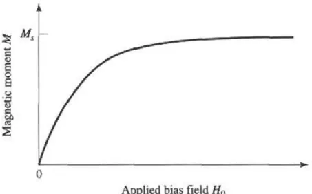
(2009)]. ... 22 Figure 2.1-1: Illustration of spinning electron with angular momentum vector [Pozar (2005)]. ... 25 Figure 2.1-2: Magnetic moment of a ferrite material versus applied magnetic field, H0 [Pozar
(2005)]. ... 27 Figure 2.1-3: Calculated dissipative components of YIG and Nickel ferrite’s complex tensor
permeability. . ... 31 Figure 2.1-4: Calculated dispersive components of YIG and Nickel ferrite’s complex tensor
permeability. . ... 31 Figure 2.2-5: Schematic of an SIW guide realized on planar dielectric substrate [Wu,
Deslandes, and Cassivi (2003)]. ... 32 Figure 2.2-6: Simulated SIW transmission line which illustrates the electric field component
of dominant TE10 mode. ... 34
Figure 2.2-7: Simulated SIW transmission line which illustrates the magnetic field component of dominant TE10 mode. ... 34
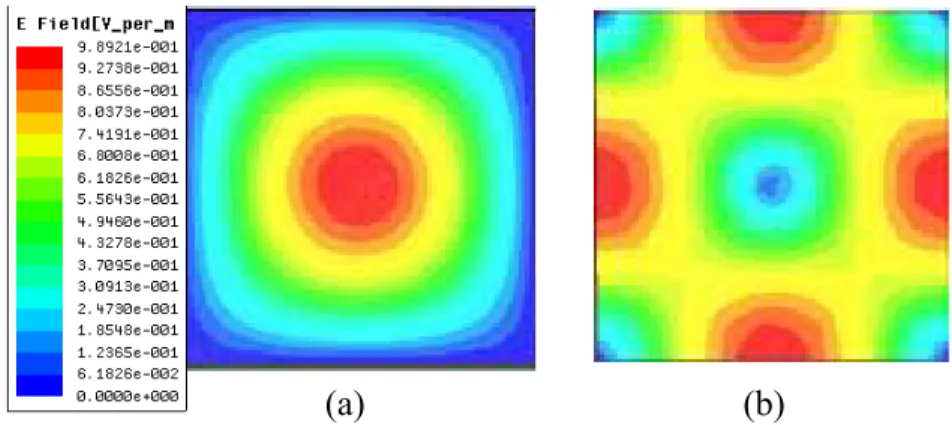
Figure 3.2-1: Top view of a simulated rectangular cavity resonator displaying (a) Electric field of dominant TE101 mode and (b) Magnetic field of dominant TE101 mode. ... 36
Figure 3.2-2: Fabricated SIW cavity resonator at 12 GHz. ... 37 Figure 3.2-3: Fabricated SIW cavity loaded with two rectangular ferrite slabs along the
sidewalls. ... 38 Figure 3.2-4: Cross-sectional view of the SIW cavity loaded with (a) a single ferrite slab and
Figure 3.2-5: Calculated relative permeability components of YIG ferrite versus applied magnetic field (H0) in Tesla, μꞌ and κꞌ are dispersive permeability components, μꞌꞌ and κꞌꞌ are dissipative loss components and μe is the effective permeability. .... 41
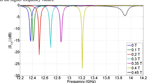
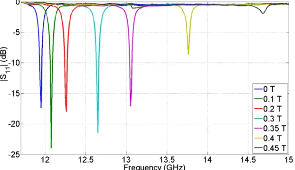
Figure 3.2-6: Measurement results displaying the resonant peaks of a single ferrite loaded cavity resonator versus frequency. ... 42
Figure 3.2-7: Measurement results displaying the resonant peaks of a double ferrite slabs loaded cavity resonator versus frequency. ... 43
Figure 3.2-8: Calculate and measured tuning curves of single and double ferrite slabs loaded SIW cavity resonator. ... 44 Figure 3.2-9: Measurement results of unloaded Q-factors and resonant frequency versus
applied magnetic bias for single and double ferrite loaded SIW cavity resonators. ... 45 Figure 3.3-10: Schematic of magnetically tunable feedback loop oscillator. ... 46 Figure 3.3-11: Multilayered SIW cavity resonator (a) Cross-sectional schematic with
Ls = 5.5 mm, Ws = 0.5 mm, Lp = 3 mm (b) Top view of the fabricated cavity with WSIW = 12 mm, CW = 1.2 mm, CG = 0.2 mm, W = 9.8 mm, L = 9.8 mm,
LT = 5.25 mm, θ = 35°. ... 47
Figure 3.3-12: Twin ferrite slabs loaded SIW section of length l1 a) schematic representation
b) equivalent transmission line model. ... 48 Figure 3.3-13: Double ferrite slabs loaded cavity resonator a) schematic representation b)
equivalent transmission line model. ... 49 Figure 3.3-14: Four ferrite slabs loaded cavity resonator a) schematic representation b)
equivalent transmission line model. ... 51 Figure 3.3-15: Top view of multilayered SIW cavity resonator containing four empty slots
for loading ferrite slabs around the periphery of the cavity with WSIW = 12 mm,
l2 = 1.0 mm, l1 = 8.8 mm, LT = 5.25 mm, θ = 35°. ... 52
Figure 3.3-17: Measured and calculated frequency tuning curves of SIW cavity resonator loaded with a single ferrite slab. ... 54 Figure 3.3-18: Calculated magnetization value of rectangular YIG prism, where the length
and width of the rectangular prism are 8.8 mm and 1 mm respectively. ... 55 Figure 3.3-19: Measurement results of multi-layer cavity resonator. ... 55 Figure 3.3-20: Plot of calculated and measured frequency tuning curves of four ferrite slabs
loaded SIW cavity resonator. ... 56 Figure 3.3-21: Fabricated multilayered magnetically tunable SIW feedback-loop oscillator (a)
top view (b) bottom view. ... 57 Figure 3.3-22: Measurement of open-loop gain and phase versus applied magnetic field H0
for a single ferrite loaded SIW cavity with ferrite width l2 = 1mm. ... 58
Figure 3.3-23: Spectrum of the magnetically tunable oscillator with SIW cavity resonator loaded with four ferrite slabs. ... 59 Figure 3.3-24: Spectrum of the oscillator output when the SIW cavity resonator loaded with
four ferrite slabs and applied magnetic bias is 0 T. ... 60 Figure 3.3-25: Oscillator frequency tuning range and phase noise performance versus applied
magnetic bias. ... 61 Figure 3.3-26: Biasing mechanism of ferrite loaded SIW cavity resonator to produce
frequency tuning and frequency modulation. ... 62 Figure 3.3-27: Fabricated single substrate ferrite loaded SIW oscillator, containing SIW
cavity loaded with two ferrite slabs and copper wires winded around the soft iron core to produce the frequency tuning and frequency modulated output, with coupling gap g = 4.5 mm. ... 63 Figure 3.3-28: Calculated and measured frequency-modulated spectrums of magnetically
tunable SIW oscillator for modulation index value mf≈1. ... 64
Figure 3.4-30: Calculated µrf of YIG ferrite, a) versus frequency at internal magnetic fields
Hi = 0 T, 0.17 T and 0.24 T, b) versus internal magnetic field Hi at frequencies
f = 9 GHz, 10 GHz and 11 GHz. ... 67 Figure 3.4-31: Calculated β, α and µrf versus frequency at applied magnetic field Hi = 0.17 T
for W = 9.8 mm and wf = 1 mm. ... 68
Figure 3.4-32: Calculated fc and fµ versus Hi for wf = 1 mm. ... 68
Figure 3.4-33: Fabricated FLSIW switch, W = 9.8 mm, L = 16 mm, wf = 1 mm. ... 69
Figure 3.4-34: Calculated and measured S-parameters for different magnetic bias (on state for He = 0 T or Hi = 0 T and off state for He = 0.3 T or Hi = 0.17 T). ... 70
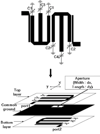
Figure 4.1-1: Simultaneous electrically and magnetically tunable cavity resonator, a) SIW cavity resonator loaded with a lumped capacitor and a ferrite slab, b) equivalent transmission line model. ... 74 Figure 4.1-2: Fabricated SIW cavity resonator with CW = 1.2 mm, CG = 0.2 mm, l2 = 5.9 mm,
l1 =1 mm, L = W = 9.8 mm. ... 76
Figure 4.1-3: Theoretically calculated resonant frequency curve of YIG planar slab and capacitor loaded SIW cavity resonator. ... 77 Figure 4.1-4: Measurement results for different lumped capacitor C and external applied
magnetic field H0 values. ... 78
Figure 4.1-5: Measurement results for two-dimensionally tuned SIW cavity resonator using a single ferrite slab and a varactor diode. ... 79 Figure 4.1-6: Two-dimensional measurement results showing variation of resonant frequency
a) versus Vb, b) versus H0. ... 80
Figure 4.1-7: Measurement results for a) |S11| (dB), b) Qu. ... 80
Figure 4.2-8: Fabricated SIW second order Tchebyscheff band-pass filter with a) Top-view W = 10 mm, w1 = 5.2 mm, w =3.9 mm, w2 = 5.2 mm, l1 =8.3 mm, l2 =8.3 mm
Figure 4.2-9: An SIW cavity resonator loaded with ferrite slabs along the two sidewalls and a capacitor at the center of the cavity (a) cross-sectional view (b) equivalent transmission line model. ... 84 Figure 4.2-10: Calculated propagation constant βf of an SIW transmission line loaded with
ferrite slabs along its sidewalls. ... 86 Figure 4.2-11: Calculated resonator slope parameter values versus applied magnetic bias (Hi). .. 87
Figure 4.2-12: Calculated results of resonator slope parameter values and constant frequency and constant bandwidths isofrequency curves. ... 88 Figure 4.2-13: Measurement results of magnetically tuned (1-D) SIW cavity filter loaded
with C = 80 fF capacitor at its center. (a) Measured S21 and S11 parameters. (b)
Enlarged S21 parameters. ... 89
Figure 4.2-14: Measurement results of 2-D tuned SIW cavity filter loaded with a) measured S21 and S11 parameters b) enlarged S21 parameters. ... 90
Figure 4.2-15: Measurement results of 2-D tuned variable bandwidth SIW band-pass filter a) Measured S21 and S11 parameters and b) Enlarged S21 parameters. ... 92
Figure 4.2-16: Measurement results of 1-D tuned SIW cavity filter using ferrite slabs a) Measured S21 and S11 parameters b) Enlarged S21 parameters. ... 93
Figure 4.2-17: Measurement results of 2-D tuned SIW cavity filter using varactor diode and ferrite slabs a) Measured S21 and S11 parameters b) Enlarged S21 parameters. ... 94
Figure 4.3-18: Fabricated SIW cavity backed antenna loaded with capacitor and ferrite slab SL =5.5 mm, SW = 1.9 mm. ... 95
Figure 4.3-19: Measured S11 parameter of cavity backed antenna with a) one dimensional
magnetic tuning b) two-dimensional electric and magnetic tuning. ... 96 Figure 4.3-20: Measured radiation pattern, in dBi, of one-dimensional magnetic tuned cavity
backed slot antenna: a) H-plane and b) E-plane. ... 97 Figure 4.3-21: Measured radiation pattern, in dBi, of two-dimensional magnetic tuned cavity
Figure 5.2-1: Simulation of a magnetic field vector inside SIW transmission line using Ansoft HFSS 15.0. Magnetic vector field illustrate the circular polarization behaviour near the SIW sidewall. ... 103 Figure 5.3-2: Fabricated tunable non-reciprocal FLSIW phase shifter with Lp = 18mm,
Wp = 1mm, θ =25°, Lslot = 3.8mm, WSIW = 6.5mm. ... 104
Figure 5.3-3: Cross-sectional view of the tunable non-reciprocal FLSIW phase shifter. ... 105 Figure 5.3-4: Calculated dispersive permeability components of YIG and Nickel (Ni) ferrite. .. 106 Figure 5.3-5: Measured insertion losses of a 2 mm wide Nickel (Ni) ferrite loaded SIW phase
shifter. Traces are plotted for different magnetic bias value ranging from 0 to 0.2 T with steps of approximately 0.05 T. ... 107 Figure 5.3-6: Measured phase shift from port 1 to 2 and from port 2 to 1 of a 2 mm wide
Nickel (Ni) ferrite loaded SIW phase shifter. Traces are plotted for different magnetic bias value ranging from 0 to 0.2 T with steps of approximately 0.05 T. ... 108 Figure 5.3-7: Measured forward and reverse phase shifts and insertion losses for different
widths of a ferrite slab, compared to phase shifts and insertion losses of an unloaded SIW. (a): phase of 1 mm Nickel ferrite slab loaded in SIW; (b): phase of 1.5 mm Nickel ferrite slab loaded in SIW; (c): phase of 2 mm Nickel ferrite slab loaded in SIW; (d): insertion losses of 1 mm Nickel ferrite slab loaded in SIW; (e): insertion losses of 1.5 mm Nickel ferrite slab loaded in SIW; (f): insertion losses of 2 mm Nickel ferrite slab loaded in SIW. ... 109 Figure 5.3-8: Measured forward and reverse phase shifts and insertion losses for different
widths of ferrite slab, compared to phase shifts and insertion losses of an unloaded SIW. (a): phase of 1 mm YIG slab loaded in SIW; (b): phase of 1.5 mm YIG slab loaded in SIW; (c): phase of 2 mm YIG slab loaded in SIW; (d): insertion losses of 1 mm YIG slab loaded in SIW; (e): insertion losses of 1.5 mm YIG slab loaded in SIW; (f): insertion losses of 2 mm YIG slab loaded in SIW. ... 110 Figure 5.3-9: Photograph of the thermal measurement set up. ... 112
Figure 5.3-10: Measured amplitude of S21 and S12 parameters of the phase shifter versus
temperature for 2 mm wide Nickel ferrite slab loaded inside the phase shifter. .. 112 Figure 5.3-11: Measured angle of S21 and S12 parameters of the phase shifter versus
temperature for 2 mm wide Nickel ferrite slab loaded inside the phase shifter ... 113 Figure 5.4-12: Topology of a four port circulator. ... 114 Figure 5.4-13: Signal flow graph representation of four port circulator. ... 115 Figure 5.4-14: Calculated S-parameters of an ideal four-port circulator. ... 116 Figure 5.4-15: Calculated S-parameters of an ideal four-port circulator. ... 117 Figure 5.4-16: Four port circulator geometry in Ansoft’s HFSS 15, Fw = 2 mm, W = 6.5 mm,
and Fl = 18 mm. ... 118
Figure 5.4-17: A snap-shot of electric field simulation of four-port circulator in HFSS 15, port 1 is the input port. ... 119 Figure 5.4-18: A snap-shot of electric field simulation of four-port circulator in HFSS 15,
port 2 is the input port. ... 119 Figure 5.4-19: Simulation results of four port circulator consisting of single ferrite loaded
gyrator in HFSS 15. ... 120 Figure 5.4-20: Simulation results of four port circulator consisting of single ferrite loaded
gyrator in HFSS 15. ... 121 Figure 5.4-21: Simulation results of improved four port circulator consisting of single ferrite
loaded gyrator in HFSS 15 (An additional phase shift of approximately 50° was added in channel A). ... 121 Figure 5.4-22: Fabricated four port circulator on Rogers 6010, 25 mil substrate with
l = 3.5 mm, and θ = 25°. ... 122 Figure 5.4-23: Photograph of the measurement set up of the four port circulator. ... 123 Figure 5.4-24: Measurement results of the four port circulator. ... 123
Figure 6.1-1: Fabricated prototypes of ferrite loaded a) HMSIW b) SIW, with FL = 15 mm,
FW = 1.25 mm, Ms = 1.97 mm, TW = 3.9 mm, W1 = 11 mm, W2 = 5.5 mm,
T1 = 5.6 mm, T2 = 1.2 mm. ... 126
Figure 6.1-2: Measured forward attenuation constant values of ferrite loaded HMSIW and SIW sections for H0 = 0 T, and H0 = 0.35 T. ... 127
Figure 6.1-3: Measured S-parameters of SIW transmission line. ... 128 Figure 6.1-4: Measured S-parameters of HMSIW transmission line. ... 128 Figure 6.1-5: Plot of f1 and f2 to find the propagation constant of ferrite loaded SIW. ... 129
Figure 6.1-6: Plot of measured values of forward and reverse phase shift of ferrite loaded HMSIW and SIW. ... 130 Figure 6.2-7: Fabricated prototypes of ferrite loaded a) SIW b) HMSIW with
FL1 = FL2 =5 mm , l1 = l2 = l3 = 3.4 mm, w1 = w3 = 0.15 mm, w2 = 0.4 mm. ... 131
Figure 6.2-8: Frequency response curves of magnetically tuned HMSIW band-pass filter. ... 131 Figure 6.2-9: Frequency response curves of magnetic and capacitive tuned HMSIW
LIST OF ACRONYMS AND ABBREVIATIONS
1-D One-Dimensional
2-D Two-Dimensional
A/D Analog to Digital AC Alternating Current
ADS Advanced Design System (Agilent)
AI Active Inductor
BST Barium-Strontium-Titanate
BW Bandwidth
CBCPW Conductor Backed Coplanar Waveguide CPW Coplanar Waveguide
DC Direct Current E-field Electric-Field
ESD Electro Static Discharge FET Field Effect Transistor
FLSIW Ferrite Loaded Substrate Integrated Waveguide
FM Frequency-Modulated
FMR Ferromagnetic Resonance GaAs Gallium Arsenide
H-field Magnetic Field
HFSS High Frequency Structure Simulator® (ANSYS) HMSIW Half Mode Substrate Integrated Waveguide IDCs Inter-Digital Capacitors
LPE Liquid Phase Epitaxy LPF Low Pass Filter
MEMS Micro-Electro-Mechanical Systems
MESFET Metal Semiconductor Field Effect Transistor MIM Metal-Insulator-Metal
Ni Nickel
PA Power Amplifier
PCB Printed Circuit Board
PIN Positive Intrinsic Negative PNA General Purpose Network Analyzer
RF Radio-Frequency
RX Receiver
SIW Substrate Integrated Waveguide
SM Surface Mount
SOLT Short Open Load Thru SPST Single Pole Single Throw
SSIW Slotted Substrate Integrated Waveguide TE Transverse Electric
TEM Transverse Electromagnetic TM Transverse Magnetic TRL Thru- Reflect-Line
TX Transmitter
UHF Ultra High Frequency UWB Ultra Wide Band
VCO Voltage Controlled Oscillators VNA Vector Network Analyser WLAN Wireless local area network
X-band Standard waveguide band from 7 GHz to 11.2 GHz YIG Yttrium Iron Garnet
INTRODUCTION
Since the past decades, there has been a significant development of electronically reconfigurable or tunable circuits, devices, and components in the field of radio frequency (RF) and microwave wireless systems, which is even now moving towards the millimeter-wave domain. This has been fuelled by the emerging needs for multi-band and multi-function specifications within the same compact-structured design platform. Indeed, current communication devices are able to offer multiple functionalities that are generally operating in different frequency bands. In addition to the popular 3G and 4G communication systems, for example, a portable handheld device also supports WLAN and Bluetooth applications. Therefore, it is obvious that wireless systems are becoming more complex and smart due to the inclusion or convergence of multiple standards and applications into a single device. In order to meet the stringent design requirements of those wireless systems, the related RF front ends must be adaptive and flexible in nature. The quality of front-end is directly responsible for the performances of the entire systems as it is directly related to critical electrical specifications of the system such as noise, dynamic range and channelization. This becomes much more involved in multi-band and multi-function systems as the performances should be consistent and uniform for all system states. An adaptive RF front end has been recognized as a viable and effective solution in incorporating multi-band and/or multi-channel circuits with multi-functions to satisfy several wireless system standards. One desirable way of realizing such multi-band or multi-channel systems is through deploying fast and tunable RF and microwave components and circuits, which should be enabled electronically. For example, a frequency agile filter with embedded tuning elements can carry out a switching function between several individual filters in order to have more than one frequency response. Compared with a bulky bank of filters, a single tunable filter offers higher flexibility, better functionality, lighter weight, and the same hardware circuitry can be used to cope with the requirement of multiple purposes, which also reduces the total cost and size.
The replacement of a large and complex circuitry with single tunable device is indeed a very attractive option. However, there are lot of complexities and issues associated with it. One of the biggest challenges of using a single tunable device that covers the multitude of functions is whether it can maintain the same device or system performance at all times or at all states. Usually, in complex systems, there are individual circuit blocks that are optimized or fine-tuned
to carry out specific functionalities. When a single block is designed to perform the same tasks that were previously taken care by a number of individual blocks, then of course, the same performance quality cannot be expected in connection with all the tasks. An example can again be taken of a tunable band-pass filter, which is designed to work continuously over a certain band of frequency. If the filter is designed only with a purpose of tuning the center frequency, it cannot be expected to display the same filter response over the frequency band. As soon as the filter is tuned from one center frequency point to another, the key design parameters that are used in optimizing the filter response change, making the filter response different from the original. Therefore, in order to maintain the best circuit or device performances throughout its tuning range, a certain design strategy must be adopted.
Figure 0.1-1: The structure of an aperture coupled constant bandwidth tunable filter [Moon, et al. (2008)].
In literature, recently there has been a significant amount of works done in the realization of fully-adaptive and reconfigurable filters. In the works carried out by [Joshi, et al. (2009)], [Yi, and Rebeiz (2011)] and [Moon, et al. (2008)] tunable band-pass filter with reconfigurable
bandwidths and center frequencies are presented. In Fig. 0.1-1 and Fig. 0.1-2, the topology of the filter structure and measurement results presented in [Moon, et al. (2008)] are illustrated.
(a) (b)
Figure 0.1-2: Measurement results of the filter illustrating (a) S21 parameters (b) S11 parameters
[Moon, et al. (2008)]
The tunable filter presented in [Moon, et al. (2008)] consists of two sections of hairpin resonators that are coupled to each other by an aperture which lies in an intermediate layer of a multi-layer substrate. The resonators are coupled through an aperture to achieve higher frequency selectivity, and to reduce the total size of the filter. The varactor diodes that are connected at the end of the resonators are used for changing the center frequency of the filter as well as to change its bandwidth. The varactor diodes connected at the end of the resonators change their equivalent length, thereby changing the resonant frequency, at the same time they are also used in changing the inter-resonator couplings to maintain the constant frequency response. The band-pass filter presented in Fig. 0.1-1 and Fig. 0.1-2, uses semiconductor varactor diodes as tuning elements. In order to realize any type of RF and microwave tunable devices, a special tuning element has to be integrated into the device circuitry. The most commonly used tuning elements include: semiconductors (varactor diodes, PIN diodes, and transistor), micro-electro-mechanical systems (MEMS), ferroelectrics materials, and ferromagnetic materials. Each of these tuning elements has their own advantages and disadvantages. Their use largely depends upon, the required type of tunability (discrete or continuous), operating power, design frequency, and also manufacturing complexity and total cost. Previously to this work, few efforts has been made in the design of tunable planar devices based on ferrite material, even if a multitude of three dimensional devices based on bulky waveguide technology has been demonstrated. One of the objectives of this thesis
is to realize fully adaptive and reconfigurable planar filters based on ferrite material as a tuning element. It is also a purpose of this thesis to realize fully adaptive and reconfigurable filters using ferrite material as a tuning element.
In this thesis, a new type of microwave tunable devices based on substrate integrated waveguide (SIW) technology is presented. The SIW based devices are made magnetically tunable by loading planar ferrite slabs inside them. It is demonstrated that, with the application of an external magnetic bias on ferrite loaded SIW (FLSW) structures, a number of interesting and very useful microwave components and devices can be realized. The designed tunable microwave components and devices could then be directly implemented in the realization of a high power radar system design. In Fig.0.1- 3 as an example, a schematic drawing of radar system is presented.
Figure 0.1-3: A schematic of radar system design
It can be seen from Fig. 0.1-3 that, an RF system is made of a number of components and devices including: signal generator, mixer, filters, low-noise amplifier (LNA), power amplifier, antenna, and circulator. In order to realize a fully adaptive and reconfigurable system design, it will be an advantage if in each of the above-mentioned components some degree of tunability can be added. This will allow the system to reconfigure itself to a new system requirement or specification
without a need to change the whole hardware circuitry. Moreover, for a high power application, it will be desirable to have these components capable of handling higher powers. Thus, it is a purpose of this thesis to develop a new type of microwave tunable components with high power handling capabilities.
SIW is an emerging transmission line technology, which is lower in cost, lower in loss, and can also handle high power than other transmission lines. Moreover, it is fully compatible with other planar circuits. Since ferrite materials are also known for their high power handling capability and high tunability, they are used together with SIW technology to realize a new type of highly tunable, planar microwave components and devices for radar application at 12 GHz.
In Chapter 1, a general overview and current status of various tuning elements and related technologies is presented. Each of the technologies is compared to one another in terms of performance, cost and applications. In Chapter 2, an introduction to ferrite material is presented with a brief theoretical review of its microscopic properties. Properties of two different types of ferrite materials to be used in this work are also presented. An introduction to SIW technology and its basic design rules are discussed. In Chapter 3, magnetically tunable microwave devices based on ferrite loaded SIW technology are presented. Tunable radar system components like resonators, oscillators, and switches are introduced. In Chapter 4, a novel concept of simultaneous electric and magnetic two-dimensional tuning is presented, where both ferrite materials and varactor diodes are used to achieve the dual electric and magnetic tuning. It is demonstrated that with the concept of two-dimensional tuning not only the total tuning range can be extended but also the key design parameters like matching, Q–factor, coupling between resonators, and filter shape can be improved. In Chapter 5, non-reciprocal microwave devices are presented, where the non-isotropic behaviour of the ferrite material is used to realize phase-shifters, gyrator and circulator. Finally in Chapter 6, half-mode SIW (HMSIW) devices are introduced. It is shown that the performance of HMSIW devices in terms of tunability and losses are very similar to SIW type of devices. Due to their miniaturized size, they can be used as an alternative to magnetically tunable SIW devices.
CHAPTER 1
TUNABLE RF AND MICROWAVE DEVICES
The current radar and wireless communication systems are becoming more and more complex in terms of performances and functionalities. Military radars for example are desired to be reconfigurable in frequency in order to avoid enemy interferences and in bandwidth to dynamically adjust their resolution depending on the target. Also, a portable hand held communication devices are not only equipped with usual voice-to-voice communication capabilities, but also they can support wireless local area network (WLAN), and Bluetooth. Thus, it is evident that, communication systems are becoming more advanced, smart and complex due to the inclusion or convergence of multiple standards and applications into a single device. In order to meet the requirements of modern wireless communication systems, the RF front ends must therefore be adaptive and flexible in nature. An adaptive RF front ends can be realized by incorporating multi-band or multi-channel circuits to satisfy the several wireless system standards. One way of realizing the multi-band or multi-channel communication systems is by incorporating the tunable microwave components, circuits and devices into them. The tunable devices can be designed to operate not just in one frequency band but in several of them. For example, a single frequency agile filter with embedded tuning elements can replace the requirement of switching between several filters to have more than one frequency response. In comparison to a fixed bank of filters, a single tunable filter is capable of switching the filter response between different frequencies, it is lighter in weight, smaller in footprint, and the same hardware circuitry can be re-used for multiple purposes, which also reduces the total cost. In some cases, the tuning or reconfigurable features are also used in the real-time adjustment of circuit parameters, which are not just limited to frequency tuning.
In order to realize the RF and microwave tunable devices, a special tuning element has to be integrated into the device circuitry. The most widely and commercially used tuning elements include: semiconductors (varactor diodes, PIN diodes, and transistor), micro-electro-mechanical systems (MEMS), ferroelectrics materials, and ferromagnetic materials. Each of these tuning elements or techniques has their own advantages and disadvantages. Their use largely depends upon, the required type of tunability (discrete or continuous), operating power, design frequency, and also manufacturing complexity and total cost. The RF and microwave systems are made up of a number of components and devices including: oscillator, antenna, phase-shifter, amplifier
etc. Each of these devices can be made tunable by incorporating any one of the above mentioned tuning elements. To cover all of the microwave tunable devices is beyond the scope of this chapter. Therefore, a general overview of each tuning element in the realization of a tunable microwave filter is only presented. Since the purpose of this thesis is to realize ferrite loaded magnetically tunable SIW devices, a comparative study of ferrite materials with other tuning elements in terms of performance, cost, and reliability is also discussed and presented.
1.1 Semiconductor tuning elements
In this section, a detailed discussion on RF and microwave tunable band-pass filters that make use of semiconductor as key building elements is presented. Semiconductor is known to be the most popular and widely used technology in the realization of fast tunable integrated RF and microwave components and circuits. They are always associated with low cost, light weight and small footprint, and most importantly they are known to offer a very wide tuning range with adaptive options, depending on diodes and transistor design platforms. However, they can only offer a low Q factor at microwave frequencies [Torregrosa-Penalva et al. (2002)]. For example, the Q factor of a varactor diode is proportional to frequency and junction capacitance at low frequencies (1 MHz) whereas it is inversely proportional at higher frequency (>100 MHz) values [Norwood, and Shatz (1968)]. Moreover, parasitic series resistance of the diode caused by packaging also increases at higher frequency. Thus, the use of varactor techniques is generally limited to frequencies below 10 GHz as they suffer from higher insertion loss. However, an attempt has been made to compensate the loss and increase the Q factor by incorporating FETs as a negative resistance device [Chandler et al. (1968)]. Of course, any active compensation can be made possible at the expense of additional power consumption and potential non-linear effects. There are basically three reported different types of semiconductor devices that are integrated inside a microwave circuit as tuning elements, which include varactor diode, PIN diode, and field effect transistor (FET). Naturally, any active diodes and transistors can be used as tuning elements, depending on their technical merits. The tuning elements are used in the realization of tunable devices that are made either in discrete mode or in continuous mode.
1.1.1 Varactor diode
Varactor diode is also known as a variable reactor, which means a device whose reactance can be made variable by the application of a DC bias voltage. The reactance in the case of a varactor diode is a simple depletion layer capacitance, which is formed at the junction of p-type and n-type semiconductor materials. Depending upon the polarity and the strength of the applied bias voltage, the depletion layer width is changed, which in turn also changes the junction capacitance value. Since the capacitance value of the varactor diode can be changed even by a slight variation of applied bias voltage, it finds application as a continuously tunable device. Varactor diodes are very useful in realizing a variety of devices including tunable filter, tunable phase shifter, and voltage controlled oscillator (VCO), parametric amplifier, and mixer. In this section, a brief overview of tunable filters based on varactor diodes are discussed and presented.
There is a growing interest in the design and realization of RF and microwave systems that have multi-channel and multi-band functionalities. Since filter is one of the most critical parts of the system design, it is highly beneficial to realize such a filter that is fully adaptive to any changes in connection with the system behaviour. Tunable filter can reduce the complexity of a system design by avoiding the need of filter banks, which consist of multiple filters with distinct filter responses for each frequency band. The use of a tunable filter allows the coverage of the whole frequency bandwidth. Early work of tunable filter designs involved the tuning of center frequency using various kinds of tuning devices and materials. Presently, the focus of a tunable filter design has not only been on changing the center frequency but also on making it fully reconfigurable in terms of bandwidth and selectivity. Varactor diode has been one of the most promising technologies that have been widely used in the realization of a wide variety of electronically tunable filters. In the early work of varactor tuned filter developments, the center frequency was tuned by loading the varactor diodes at the ends of resonating stubs [Hunter, and Rhodes (1982)]. It was noticed that, the band stop characteristic of the filter was largely dependent upon the coupling gap between the feeding transmission line and the parallel stubs. Since the coupling gaps of the parallel stubs are highly frequency dependent, it was suggested in [Hunter, and Rhodes (1982)], to tune the capacitance of the gaps in accordance with the tuning capacitances in order to preserve the band stop characteristics. In [Makimoto and Sagawa (1986)], a varactor tuned ring resonator filter using microstrip technology was presented. The center frequency of the filter was configured by changing both
filter’s coupling and tuning capacitances. In [Musoll-Anguiano et al. (2002)] a fully adaptable band stop filter, which is able to reconfigure its center frequency, bandwidth, and selectivity, was demonstrated. The bandwidth tuning is achieved by varactor diodes that are used in coupling resonators to transmission line, whereas the center frequency is controlled by varactor diodes connected at the end of transmission line resonators.
Since the varactor diodes are made up of semiconductor materials, they suffer from non-linearity when injected with high power signals. Despite non-linear behaviours of semiconductor materials, it has been demonstrated that the varactor diodes can also be used for realizing high power filters [Swartz et al. (1980)] at UHF band. Recently, a varactor tuned band-pass filter with improved linearity has been presented in [Yu et al. (2012)]. The filter topology consists of an open-ended transmission line with back varactor diodes loaded at one end. The back-to-back varactor diodes enhance the linearity of the filter while the mixed electric and magnetic coupling scheme keeps the absolute bandwidth at a constant value when the frequency of the filter is tuned. Thus, varactor diode presents itself a very promising low cost, highly tunable, and adaptive semiconductor tuning element that can be used in realizing tunable filters at relatively low tuning voltage.
1.1.2 PIN diode
Figure 1.1-1: Photograph of the fabricated switchable band-pass filter [Brito-Brito, et al. (2008)]. PIN diodes are semiconductor based tuning devices, which are popularly used to produce discrete states reconfigurable filters. In this section, a brief review of tunable filters based on PIN diodes is presented. In [Lugo, and Papapolymerou (2004)], a PIN diode based reconfigurable filter for
wireless applications was demonstrated. The designed filter falls into a category of admittance inverter coupled resonator filter, with two discrete bandwidths at 5.6 GHz
The PIN diodes being semiconductor device, non-linear effects of the diode in the filter structure are also studied. In [Brito-Brito, et al. (2008)], a band-pass filter which is switchable between two central frequency states is presented. The designed filter uses PIN diodes for switching, such that in each frequency states a constant bandwidth is maintained. In Fig. 1.1-1, the fabricated prototype of the switchable band-pass filter is illustrated. By changing the polarity of the bias voltage, the filter is switched between 1.5 GHz and 2 GHz center frequencies respectively [Brito-Brito, et al. (2008)]. In [Karim, et al. (2009)] a miniaturized reconfigurable and switchable band pass filter is presented. By shorting the open stubs of the filter using PIN diodes, the UWB filter is reconfigured from band-pass to bandstop response. Moreover, with the addition of half-wavelength stub to the existing reconfigurable filter, it is switched from UWB to 2.4 GHz narrowband filter response.
Figure 1.1-2: Fabricated SIW filter with via posts islands for the connection of PIN diodes [Armendariaz, Sekar, and Entesari (2010)].
A new type switchable band-pass filter based on SIW technology and using PIN diodes was presented in [Armendariaz, Sekar, and Entesari (2010)]. The two-pole band-pass filter is switched between six states ranging from 1.55 GHz to 2.0 GHz. The SIW cavity resonators are equipped with multiple via posts, which are either connected or disconnected from the top metal layers using PIN diodes, thus producing different switching states (see Fig. 1.1-2). Another SIW based
digitally tunable band-pass filter was demonstrated in [Sirci, Martinez, and Boria, (2013)], where discrete frequency tuning with nearly 8 equal spaced frequency responses from 4-4.4 GHz is obtained. In [Bakhit, and Wong (2013)], switchable band-pass filter using stepped impedance resonator was presented. The designed operates between two states, in the first stated the filter produces a band-stop response. By switching the PIN diodes to ON state, the filter response then changes from band-stop to all-pass filter characteristics.
1.1.3 Transistors
In [Lin, and Itoh (1992)], using the concept of three-terminal MESFET varactor tunable active band-pass filter was demonstrated. In the two pole filter configuration, one transistor is used to provide center frequency tuning, while the other is used to provide the negative resistance to the circuit. The negative resistance of the transistor improves the overall Q factor and improved filter response. In [Torregrosa-Penalva, et al., (2002)], a wideband tunable combline filter using gallium arsenide field effect transistor as a tuning element was presented which is illustrated in Fig. 1.1-3. The filter resonators are loaded with field effect transistors to produce the desired tunability. A systematic approach in designing tunable combline filters and the non-ideal effects in the overall performance of the filter are also discussed.
In [Pantoli, Stornelli, and Leuzzi (2012)], a high Q tunable filter with a single transistor active inductor (AI) was presented. The first order band-pass filter has a central frequency of 2400 GHz, the total frequency tuning range is 100 MHz.
1.2 MEMS techniques
Although it has been studied since early 60s, MEMS has become an emerging technology that is very useful in realizing variable capacitors, switches, and reconfigurable RF and microwave devices. Compared with semiconductors, ferrites and ferromagnetic materials based tunable devices; MEMS techniques offer much higher Q factor with very low power consumption. Moreover, as opposed to the solid state devices, they offer linear signal transmission with low signal distortion. Hence, MEMS have attracted much attention, which present very promising scheme in realizing a wide range of RF and microwave tunable components and devices. Tunable filters, realized using MEMS technology generally make use of MEMS switch or MEMS varactors as tuning elements. This section show several filter topologies to produce discrete and continuous tuning of the filter parameters.
1.2.1 Tunable filters using MEMS switches
MEMS switches are generally used for re-routing RF signals and also they are widely used in realizing tunable filters. Since MEMS based switches operate in only two states: on and off, the tunability of filters designed using MEMS switches are discrete in nature. From the structure point of view, such switches are either cantilever types or bridge types. An example of cantilever type MEMS switch is illustrate in Fig. 1.2-4.
(a) (b)
Figure 1.2-4: Schematic of electro-statically actuated cantilever type RF MEMS switch (a) OFF state (b) ON State [Ocera, et al. (2006)].
The electrical performance of a cantilever type switch largely depends upon the quality of contact in the ON state as illustrated in Fig. 1.2-4(b). There are basically two types of electrical contacts used in MEMS switches: direct contact and contact through a capacitive membrane also known as Metal-Insulator-Metal (MIM) contact. Compared to the MIM contact, the direct contact switches have lower insertion loss and better isolation. However, due to direct contacts between metals, the direct contact switch suffers from metal corrosion and has a shorter life time compared to MIM switches. Two well-known problematic issues in the development of MEMS devices are related to high actuation voltage and relatively low speed because of a mechanical process. In addition, MEMS techniques may not be well suitable for high-power applications even though significant research efforts have been invested to remedy this situation.
(a) (b)
Figure 1.2-5: Schematic of electro-statically actuated cantilever type RF MEMS switch (a) layout of the filter (b) simulation and measurement results illustrating three states of tuning [Chan, et al. (2012)].
In this section, tunable filters using direct and MIM contact based MEMS switches are presented. The cantilever type MEMS switch illustrated in Fig. 1.2-4 was used to realize a tunable hairpin line filter in [Ocera, et al. (2006)]. The filter tunability is achieved by loading identical MEMS switches at the end of hairpin resonators. When the switches are changed between on and off states, the equivalent electrical lengths of resonators is also changed, thereby making the filter
tunable. Another example of tunable filter using MEMS switch was described in [Chan, et al. (2012)], where the microwave filter is switched between three states. It is a good example in which MEMS switches are used in controlling the resonant frequency, input/output couplings, and couplings between resonators to achieve a fully-reconfigurable band-pass filter at microwave frequency. The measured filter response shows three different states of filters at 8, 9 and 10 GHz respectively. In Fig. 1.2-5(a), the filter layout with tuning elements is presented, and its simulation and measurement results are presented in Fig. 1.2-5(b)
A new type of tunable filter based on SIW technology was presented in [Sekar, et al. (2011)]. The filter topology consists of two SIW cavities that are coupled to each other via an iris window. Commercially available packaged RF MEMS switches are surface mounted in each cavity to tune them separately. The two-pole filter implemented using two-layer SIW circuit has a total tuning range of 28% with reflection loss better than 15 dB. The fabricated filter prototype and the measurement results are illustrated in Fig. 1.2-6 and Fig. 1.2-7 respectively.
Figure 1.2-6: Fabricated tunable low pass filter using direct contact MEMS switches [Sekar, et al. (2011)].
A coplanar waveguide based fully reconfigurable filter was presented in [Park, et al (2005)]. The filter topology consists of cascaded CPW-based periodic structures which are loaded with MEMS switches for tunability. By suitable combination of MEMS switches a 3-unit CPW lines are combined to form a single-cell low pass filter. In this way the length of the filter is increased by
three-times the original length, and subsequently reducing the low-pass cut-off frequency also by three-times. In a similar way, a reconfigurable band-pass filter was also realized in [Park, et al (2005)], where three band-pass units are cascaded together using MEMS switches to realize a single larger band-pass filter having a filter response at low frequency region.
(a) (b)
Figure 1.2-7: Measurement results of tunable band-pass pass filter [Sekar, et al. (2011)].
1.2.2 Tunable filters using MEMS switch capacitors
Figure 1.2-8: Lumped element filter using MEMS switch capacitors for tuning (a) fabricated prototype (b) equivalent circuit [Kim, J-M., et al. (2006)].
In this section, an overview of tunable filters based on MEMS switch capacitors is presented. Similar to the direct contact counterparts, the switch capacitors can also be cantilever or bridge
type as illustrated in Fig. 1.2-4. However, in the MEMS switch capacitors, an electrical connection is established not through an ohmic contact but through a capacitive membrane. Therefore, the switch operates between two different capacitance values: one for the ON state and the other for the OFF state. A central frequency and bandwidth controlled filter using MEMS cantilever type capacitive switch was presented in [Fourm, E., et al. (2003)]. The switches are loaded at the end of the coplanar resonators to achieve two center frequency states. The MEMS switch capacitors are also used in realizing the lumped element type tunable filters. A lumped element type tunable filter using MEMS capacitive switch was designed in [Kim, J-M., et al. (2006)] for WLAN applications. The filter is designed to select alternate frequency bands which are at 2.4 and 5.1 GHz. In Fig. 1.2-8, the fabricated prototype of the lumped element filter and equivalent circuit is illustrated.
1.2.3 Tunable filters using MEMS varactors
Figure 1.2-9: Fabricated tunable band-pass filter [Zhang, Deng, and Sen (2013)].]
MEMS varactors present an advanced form of MEMS capacitive switches. Similar to the MEMS capacitive switches, they are also composed of capacitive membrane between the two metal contacts. Unlike the capacitive switches that operate only between ON or OFF states, MEMS varactor capacitance membrane can be tuned continuously with an applied analog voltage. From the operation point of view, they are very similar to semiconductor biased varactor diodes and are useful in realizing the continuously tunable RF/microwave filters. They are more attractive than semiconductor varactor diodes in terms of Q factor, power consumption and linearity. However,
they have lower tuning speed and are more sensitive to environmental conditions for example temperature, moisture and vibrations. A lumped element type tunable K-band filter using MEMS bridge varactor was presented in [Kim, Lee, Park, and Kim, (2005)]. The filter consists of J- inverters and shunt-type resonator sections. The variable capacitors are loaded in the shunt type resonators to vary the center frequency of the filter.
In [Abbaspour, Dussopt, and Rebeiz, (2003)] a distributed type band-pass filter was designed using bridge type MEMS varactors. The coplanar transmission line is loaded with MEMS varactors to reconfigure the center frequency of the filter. A coplanar waveguide tunable band-stop filter using RF MEMS variable capacitor was presented in [Zhang, Deng, and Sen (2013)]. The filter is designed to operate from 8.5 to 12.3 GHz with 35% of tunability. This filter is another example of MEMS varactors loaded distributed type of filter. In Fig. 1.2-9, the fabricated prototype of the filter is presented.
1.3 Ferroelectrics
Figure 1.3-10: Photographs of (a) fabricated 2-pole filter and (b) area around CPW line loaded with BST [Papapolymerou, et al. (2006)].
Ferroelectrics are one of the most promising materials in realizing electronically tunable RF and microwave components and circuits for wireless front-end applications. A number of tunable devices including phase shifters, oscillators, and filters have been demonstrated by using ferroelectric materials as key tuning elements. The dielectric constant of ferroelectric materials

![Figure 1.4-14: Schematic of tunable microwave band-stop filter based on FMR [Tai, and Qiu (2009)]](https://thumb-eu.123doks.com/thumbv2/123doknet/2322484.29391/49.918.283.705.278.546/figure-schematic-tunable-microwave-band-stop-filter-based.webp)
![Figure 2.2-5: Schematic of an SIW guide realized on planar dielectric substrate [Wu, Deslandes, and Cassivi (2003)]](https://thumb-eu.123doks.com/thumbv2/123doknet/2322484.29391/59.918.207.750.511.776/figure-schematic-realized-planar-dielectric-substrate-deslandes-cassivi.webp)