an author's http://oatao.univ-toulouse.fr/23148
Ho, Caroline and Dehoux, Anita and Lacroix, Loïc and Alexis, Joël and Dalverny, Olivier and Châtel, Sébastien and Faure, Bruce Mechanical adhesion of SIO2 thin film on a polymeric substrate under compressive stress. (2016) In: XXXI International Conference on Surface Modification Technologies (SMT31), 5 July 2016 - 7 July 2016 (Mons, Belgium).
MECHANICAL ADHESION OF SIO
2THIN FILM ON A POLYMERIC
SUBSTRATE UNDER COMPRESSIVE STRESS
C. Ho
a,b, A. Dehoux
b, L. Lacroix
a, J. Alexis
a,*, O. Dalverny
a, S. Châtel
b, B. Faure
ba Laboratoire Génie de Production ENIT-INP, University of Toulouse 47 Avenue d’Azereix, 65000 Tarbes, France
b Thin Films Group, R&D Physico-Chemistry, Essilor International 39-69 Bd Jean Baptiste Oudry, 94000 Créteil, France
Abstract
To ensure good adhesion between a 200 nm silicon dioxide layer and a 4.5 μm thick hardcoat polymeric coating, a better understanding of mechanisms of adhesion at this interface is needed. To reach this purpose, quantification of adhesion is performed by analyzing SiO2 buckle morphologies generated under compressive stress. This adhesion test was chosen for its representativeness of defects observed in real life. Interfacial toughness can be determined by applying Hutchinson & Suo model. This analytical model involves accurate value of elastic modulus Ef of SiO2 thin film. Small dimensions at stake make characterization of elastic modulus challenging. First part of the study focuses on using both nano-indentation and AFM to attempt assessment of SiO2 thin film elastic modulus. Results showed significant influence of substrate for both techniques. Impact on mechanical properties between SiO2 thin films with different intrinsic stresses was also investigated and suggests that higher density of SiO2 thin film leads to higher elastic modulus. Compression tests resulted in formation of straight-sided buckles that evolve into telephone cords upon unloading. Numerical simulation and Digital Image Correlation were implemented to ensure homogeneous strain of substrate and favor regular distribution of buckles. Values of energy release rates of SiO2 / Hardcoat range from 2.7 J/m² to 8.9 J/m², depending on moduli values found on wafer or lens substrate.
Keywords
:
Oxide thin film, polymer substrate, mechanical properties, adhesion1. Introduction
Ophthalmic lenses are made of plastic polymeric substrates usually coated with functional treatments composed of 5 to 15 layers, ranging from micrometers to nanometers. The first treatment consists of a primer, conferring impact resistance properties to the lens. A hardcoat with nanoparticles, is then deposited on top of this primer, bringing anti-scratch properties to the system. Both primer and hardcoat are within the micrometer scale and are deposited by wet chemical methods. Nanometric anti-reflective stacks are then evaporated onto the hardcoat by vapor deposition technology, to enhance wearers’ comfort. Interface quality is essential to ensure stability and durability of ophthalmic multi-layer. In fact, insufficient adhesion between layers causes higher susceptibility to emergence of defects or delamination. Occurrence of these phenomena affects wearers’ comfort and has tremendous impact on products’ lifetime. Therefore, it is essential to develop a method enabling quantitative assessment of interface quality, which will ultimately enable higher product reliability.
General behavior of whole system must be fully characterized. To reduce the complexity of this characterization, focus is first placed on studying the interface between the anti-reflective stack and the hardcoat. More specifically, this paper centers around the SiO2 thin film / hardcoat interface, which is particularly sensitive because of mechanical and dimensional contrast between both parts.
This entails studying both materials composing each layer and interface. Interface quality can be evaluated through quantification of adhesion energy. Over 300 adhesion tests are referenced in the literature by Mittal (1995). Techniques commonly used on similar structures – 200 nm thick rigid thin film on soft substrate –
include cross cut, peel, scratch, 3-point and 4-point bending, Superlayer, Lasat, bulge, tensile and compression
tests. Among these numerous techniques, several methods have been implemented to study adhesion of SiO2 thin
film on polymeric substrate. Fateh (2013) performed cross-cut tests to rank adhesion of mixed metal oxide (TiO2/SiO2) thin films on polycarbonate substrate. Lian (1995) used a tape test to evaluate peel strength of SiO2
(100 nm) on PMMA to be between 56 to 552 g.cm-1, depending on deposition conditions and surface treatments.
Tadanaga (1996) also chose peel adhesion test, but was limited by fracture of Nylon-6 substrate before interfacial delamination. Amendola (2008) performed scratch tests to determine critical load of 3.4 mN ± 0.2 mN for a 100 nm SiO2 layer delamination from untreated polymeric AcryLite™ substrate. Letterier (1997)
performed tensile tests on a 12 µm PET substrate coated with 100 nm SiOx (x = 1.6). Depending on occurrence
of thermal treatment, interfacial shear strength of SiO2 / PET ranges from 66.8 MPa to 75.5 MPa. Litteken (2003) uses 4-point bending adhesion test to estimate energy release rate Gc of 200 nm thick SiO2 thin film deposited on 0.25 µm polymeric PAE SiLK™ substrate. The authors measured an adhesion value of 12 J/m², which is higher than bulk fracture resistance of SiO2 and suggests plastic deformation.
Choice of appropriate method to access adhesion is made according to compatibility with system under study, repeatability, ease of implementation, cost effectiveness and representativeness of defects observed in real life versus defects generated by mechanical tests. Chosen method should not only allow ranking of adhesion, but also give information on critical interfacial stress or even adhesion energy. Preliminary testing consisted in attempting to generate spontaneous delamination of studied SiO2 thin film using a Zirconium Superlayer. This trial was ineffective, which attests a strong adhesion at SiO2 / Hardcoat interface. Pull-off tests and three-point bending experiments have also been performed. Results located weakest interface at SiO2 thin film / adhesive and SiO2 thin film / stiffener interface respectively. This exposes challenge of finding appropriate stiffener or adhesive for strong adhesion interface. This is the reason why pull-off tests and three-point bending experiments were not favored. Considering specifications required for choice of adhesion test and preliminary testing, compression tests appear to be the most promising to characterize our structure. Compression tests of metallic thin film on polymeric substrate are indeed largely used in the literature to characterize thin film adhesion, as studied by Coupeau (1999), Cleymand (2002), Xue (2014), Cordill (2014) or Jia (2013). Few authors have applied compression adhesion tests to non-metallic thin films. Abdallah (2006) studied buckle morphologies of 400 nm thick Si3N4 deposited on hardcoat on top of AcryLite™ substrate. Evaluation of interfacial properties of oxide thin film deposited on polymeric substrate by compression tests have not been implemented yet and sets the framework of the present study. Buckling of SiO2 thin film has already been proven possible in the literature. Nicu (1999) and Fang (1999) have independently generated buckling of free-standing SiO2 micro-bridges in order to determine residual stress of thin film. Considering mechanical contrast between SiO2 thin film and polymeric substrate, inducing interfacial delamination of system under compressive stress is theoretically feasible. Besides, this technique has the advantage of applying uniaxial stress without mechanical contact in the area under observation.
As mentioned earlier, emphasis is also placed on determining mechanical behavior of each material as mechanical properties are needed to fully understand fracture energies. Nano-indentation, largely influenced by Oliver and Pharr (1992) is widely used to determine mechanical properties of both bulk materials and thin films deposited on substrate. However, impact of substrate is inevitable for thin films of a couple of nanometers thick. To limit this effect, corrections of substrate’s influence using FEA exist, as studied by Li (2009) and Hay (2011). Another approach consists in using an alternative technique with better surface detection which results in a more confined interaction volume, which is expected to lead to a lower impact of substrate. AFM is a particularly well suited technique for topography and surface roughness information. Nevertheless, several studies have used
AFM, Hopf (2014) and Trtik(2012), to extract mechanical properties of sample of interest. Elastic modulus can
indeed be determined using DMT contact model with slope of retract curve. As mentioned earlier, this alternative method to characterize elastic modulus has the advantage of having higher sensitiveness to surface detection compared to nanoindenter. However, limitations of mechanical characterization by AFM include sensitiveness to topography, cantilever spring constant and tip contact area uncertainties. In the present study, elastic modulus of SiO2 thin film deposited on Si wafer and ophthalmic lens substrate are characterized by both nano-indentation and AFM Peak Force® method. Micro-compression results to quantify SiO2 / hardcoat adhesion, are also presented.
2. Materials and Methods
2.1. Multilayer system under study
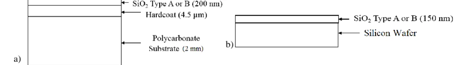
SiO2 Type A and SiO2 Type B are deposited by evaporation under vacuum whether on silicon wafer (280 µm thick and 2 inches diameter wafers from ITME) or on top of standard ophthalmic structure: 4.5 μm composite polymer referred to as hardcoat, on a 2 mm polycarbonate substrate. That is a total of four sample configurations, as represented in Figure 1.
Figure 1: Samples’ Configuration a) on polymeric substrate b) on Silicon Wafer substrate
Deposition of both types of SiO2 layers is conducted under a pressure of 8.10−5 to 1.5×10⁻⁴ mbar, similarly to Roisin (2012). Difference between SiO2 Type A and B results from supply of gas during deposition: SiO2 Type A is deposited along with oxygen gas whereas SiO2 Type B deposition does not involve introduction of additional gas. This difference in process was proven to effectively generate different levels of intrinsic stress within SiO2 layers, due to increase of porosity related to gas scattering during deposition, as suggested by Scherer (1996).
2.2. Mechanical properties of SiO2 thin film Determination of intrinsic stress
Compressive intrinsic stress of SiO2 Type A on glass strip (60 mm x 5 cm x 150 µm) was measured to be roughly -100 MPa, compared to -400 MPa for SiO2 Type B. Bending curvature of glass strip was measured before deposition of SiO2 thin film on KLA Tencor P16+. Glass strip was then placed into evaporation under vacuum chamber (glass strip being only clamped on one end, the other end remaining free) to receive deposition of SiO2 thin film. Another measurement of glass strip’s bending curvature was performed 2 hours after deposition. Compressive intrinsic stresses are then calculated using Stoney’s equation. Stoney (1909) uses bending curvature of glass strip before and after deposition of SiO2 thin film:
σ
f= −𝐸
𝑠 ℎ𝑠² (1−𝜈𝑠)ℎ𝑓1
𝑅
(1)
Where Es is Young modulus of substrate, hs and hf are substrate and film thickness respectively, 𝜈𝑠is substrate’s Poisson coefficient and R is radius of curvature.
Nano-indentation
Four sample configurations were characterized with a Nanoscope XP III from MTS, using a DCM measuring head and Berkovich diamond tip. A matrix of 30 indents separated by 30 μm, was created for each configuration. Before carrying out nano-indentation tests, tip area was first calibrated with a sample of fused silica. Continuous Stiffness Mode (CSM) which consists in overlapping a small amplitude oscillation at 75 Hz to a load controlled system, was used. Using Oliver and Pharr (1992) model, both elastic modulus and hardness can be extracted directly from nano-indentation curve, plotting load versus displacement into surface.
AFM
Four sample configurations were characterized by AFM using Peak Force® QNM mode on a Bruker’s Dimension Icon. AFM tip radius has been calibrated using fused silica of known elastic modulus. Cantilever’s spring constant of 436 N/m has been given by tip provider. Cantilever with high spring constant has been chosen for its suitability with hard materials. Several Peak Force values have been tested to determine the optimal Peak Force to apply on this specific sample. Using DMT model, developed by Derjaguin et al. (1975), elastic modulus can be determined with slope of retract curve, Poisson coefficient of film 𝜈, radius of indenter R and indentation depth δ.
(2)
𝐹 − 𝐹
𝑎𝑑ℎ=
4
3
𝐸
(1 − 𝜈)
√𝑅 𝛿
3/2 a) a) b)2.3. Adhesion test
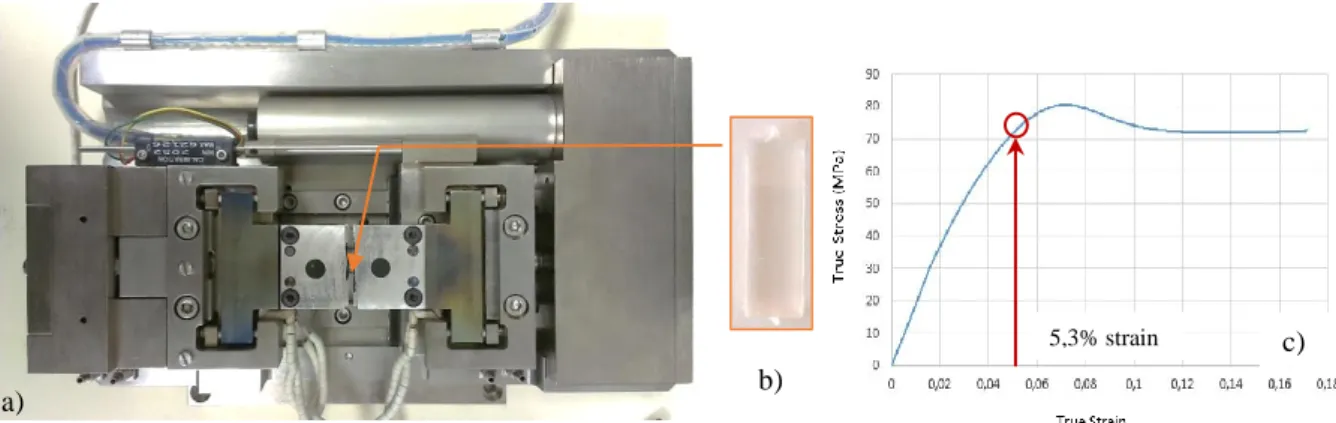
2.3.1. Experimental set-up Compression stage
Configuration of SiO2 Type A and B on lens structure was tested. Micro-compression tests were performed on a
Deben stage with a 5 kN load cell, used under compression mode (Figure 2). Motor speed was set to 0.2 mm/min. Buckling phenomena were observed and recorded using an Olympus BX51W1 optical microscope with a magnification of 5. Observation area under these conditions was 1.7 x 2.3 mm². Since displacement measurement is not close to sample and test apparatus inevitably undergoes deformations, preliminary tests are needed to estimate true strain of substrate to generate buckling on sample SiO2 B. A strain of 5.3%, below softening point (Figure 2c), was measured by video extensometer from each clamping jaw and seems to be sufficient to buckle studied SiO2 thin film.
Dimensions of sample
Buckling of compressed beams analytical calculations were made to define geometries in order to avoid buckling of substrate. As reported by Fanchon (2016), slenderness 𝜆 is defined as followed:
𝜆 =
𝐿 √𝐼𝑆=
𝐿 √ℎ2 12 (3)With 𝐿, length of sample along the compression axis, 𝐼 moment of inertia equals 𝑏ℎ123
For sample dimension of (Length: 15 mm, Width: 5 mm, Thickness: 2 mm), slenderness was calculated to be 8.7, which was then compared to critical slenderness 𝜆𝑐 :
𝜆
𝑐= 𝜋√
𝑅𝐸𝑒 (4)
With 𝐸, elastic modulus of polycarbonate substrate and 𝑅𝑒, its yield strength. Elastic modulus of polycarbonate and yield strength was determined to be 2300 MPa and 34 MPa respectively, which gives a critical slenderness of 26. As 𝜆 < 𝜆𝑐, buckling of substrate is not expected with these sample dimensions. Samples were then precision machined on a Charly Robot milling machine, with a 2 mm diameter milling cutter.
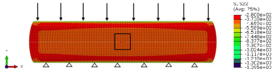
Homogeneity of deformation
Inhomogeneity on the surface can occur due to friction phenomenon between sample and clamping jaws. To determine homogeneous area of the examined surface, a finite element model of macroscopic polycarbonate substrate was built. A 3D quasi-static mechanical model was used to simulate full sample with infinite friction with clamping jaws (the most unfavorable case). Polycarbonate substrate is modeled with an elasto-plastic law (𝐸 = 2.3 𝐺𝑃𝑎, 𝜈 = 0.37, 𝜎𝑦= 34 𝑀𝑃𝑎). Boundary displacement along 𝑦
⃗
was used as load and applied on top face while bottom face remained clamped. Part was meshed with 20-node quadratic brick with reduced integration elements (C3DR20 in Abaqus® FEM software). Results of numerical model (Figure 3) give deviation fromb)
c) a)
Figure 2 : Experimental set-up of compression test a) Compression stage b) Compression sample c) compression curve 5,3% strain
homogeneity of stress of less than 1 MPa within the area of interest. As stress state is sufficiently homogeneous, we could expect a regular distribution of buckles in the observed zone.
Figure 3: Stress along the compression axis (arrows represent direction of applied displacement, triangles represent clamping condition of bottom face and rectangles represent area of interest)
Determination of local strain with Digital Image Correlation
Strain field in substrate subjected to uniaxial compressive deformation is studied by Digital Image Correlation using 2M cameras coupled with ARAMIS software. A subset size of 20 pixels with a step of 10×10 pixels is chosen. Strain field within area of interest, marked in grey in Figure 4 is 5.2 ± 0.2 % at strain levels necessary to study buckling phenomenon. Small standard deviation measured ensures strain homogeneity of 95% in the observation area.
Figure 4: Digital Image Correlation measured of strain homogeneity during a compression test. Maximum variation in the observation area reaches 0.2 %
2.3.2. Analytical model for straight-sided buckles
The critical compressive biaxial stress at the onset buckling σB0 is expressed as followed
:
𝜎
𝐵0=
12 𝜋² 1−ѵ²𝐸𝑓(
ℎ𝑏)
2(5)
where h is thickness of film, b is half width of buckle and Ef is plane strain modulus of film, as stated by Moon (2004). Energy release rate G along the sides of the buckle can be estimated by studying on one hand, the average energy per area in the unbuckled state U0 and on the other hand, the average energy per area in the buckled state U, through the relation: G = U0 – U. Expressed differently, the energy release rate G is the energy per area needed to separate SiO2 thin film from substrate over the width of buckle and is defined as:
𝐺 = 𝐺
0(1 −
𝜎𝐵0 𝜎𝑟)
2
(6)
with G0, the available energy per area stored in the unbuckled film:
𝐺
0=
(1−ѵ𝑓 2)𝜎𝑟2ℎ
2𝐸𝑓
(7)
with 𝜎𝑟, the residual stress in the buckled plate:
𝜎
𝑟=
34𝜎
𝐵0(
ℎ²𝛿²+ 1)
(8)
0 20 40 60 80 100 120 140 160 0 100 200 300 M o d u lu s (G P a)
Displacement Into Surface (nm) b)
The total stress in the film is defined as the sum of internal residual stress due to process 𝜎𝑖, and of externally applied stress ∆σxx, generated during the experiment, as stated by Jia (2013):
∆σ
𝑥𝑥=
𝐸𝑓 𝐸𝑠1−ѵ𝑓ѵ𝑠
ѵ𝑓2
𝜎
𝑒𝑥𝑡(9)
Where Ef and
ѵ
f, Es andѵ
s are elastic modulus and Poisson’s ratio of film and substrate respectively, σext the external stress applied to substrate during testing.3. Results and Discussion
3.1. Elastic Modulus of SiO2 thin film
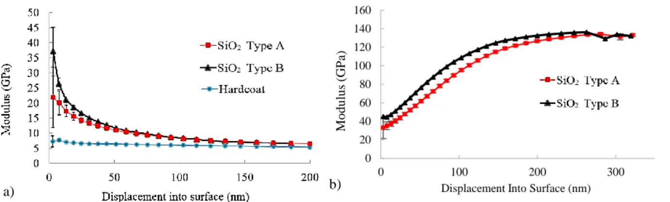
As shown in Figure 5, modulus of hardcoat is measured to be between 6 – 7 GPa by nano-indentation. It can be noted that modulus is relatively stable over a wide range of indentation depths; except for the first 10 nm, where surface detection can be particularly sensitive on a composite polymer. On the contrary, rapid evolution of modulus of SiO2 thin film as a function of displacement into surface is observed. This confirms that substrate’s influence has a considerable impact on SiO2 thin film’s modulus measurement.
Figure 5: Moduli of SiO2 film deposited on hardcoat on polycarbonate substrate (a) and on silicon Wafer (b)
Models to correct substrate’s impact relying on FEA to precisely determine contact radius, have not been implemented as it requires mechanical properties of material to characterize. It should be noted that moduli obtained for indentation depths below 20 nm are susceptible to surface detection errors. Above 30 nm indention depth, substrate’s influence becomes significant. Moduli are therefore averaged for indentation depths between 20 and 30 nm, even though impact of substrate is already existent and acknowledged (Table 1).
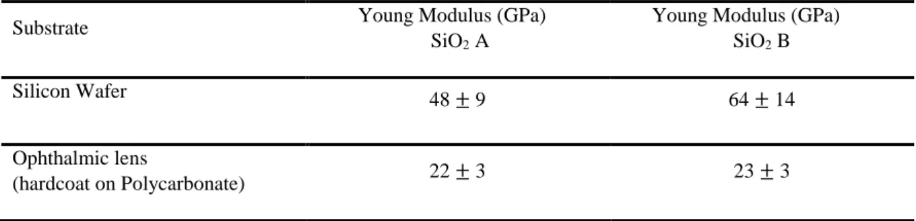
Table 1: Elastic moduli of SiO2 Type A and B deposited on Wafer and ophthalmic lens, obtained by nano-indentation
Substrate Young Modulus (GPa)
SiO2 A
Young Modulus (GPa) SiO2 B
Silicon Wafer 46± 2 58 ± 1
Ophthalmic lens
(hardcoat on Polycarbonate) 14 ± 1 17 ± 0
On both Si wafer and lens substrates, SiO2 Type A and B are differentiable. Modulus of SiO2 Type B is 26% higher than modulus of SiO2 Type A on Si wafer. The same trend is observed for lens substrate, difference being slightly lower (21%). Scherer (1996) showed that intrinsic stress is linked to local density – without porosity taken into account - through Si-O-Si deformation; diminution of bond angle at the O atom site, being related to increase in intrinsic stress. This could explain difference observed between SiO2 Type A and B; change of material density leads to a higher intrinsic stress and also to the modification of mechanical properties. Even a)
though this range is extremely wide, we can conclude that true value SiO2 lies somewhere between 14 GPa and 46 GPa for SiO2 Type A and between 17 GPa and 58 GPa for SiO2 Type B. Scherer (1996) also determined
moduli of 120 nm SiO2 thin film deposited by electron-beam evaporation on glass substrate. Values range from
35 GPa for deposition without additional gas (similar to SiO2 Type A) to 48 GPa (similar to SiO2 Type B) for deposition with oxygen, which is within the range of moduli measured.
Moduli of SiO2 thin film measured on Si wafer are significantly higher (~250%) than those on lens. According to curves presented on Figure 5, elastic moduli of SiO2 are overestimated on Si wafer and underestimated on lens substrate. Aside from contribution of substrate’s influence, outgassing of lens substrate may explain lower moduli compared to those found on Si wafer. Moreover, during deposition, thermal stress could be generated on polymer substrate due to heat load of electron beam. Given that coefficient of thermal expansion of SiO2 and polymer are significantly different, this may result in change of dimension of polymeric substrate, which might ultimately impact SiO2 modulus value. Another explanation could come from difference of microstructure between SiO2 layers deposited on two substrates of different nature.
Characterization of mechanical properties by AFM were performed using a Peak Force value of 1000 nN, which has been chosen to have an elastic deformation value around 2 nm, corresponding to 1% thickness of SiO2 layer. Deformation depth was estimated to be 1.9 ± 0.3 nm. This was obtained by analyzing deformation map over the same 1 µm² area.Modulus and its standard deviation for each sample configuration are summarized in Table 2.
Table 2: Elastic moduli of SiO2 Type A and B deposited on Wafer and ophthalmic lens, obtained by AFM
Substrate Young Modulus (GPa)
SiO2 A
Young Modulus (GPa) SiO2 B
Silicon Wafer 48 ± 9 64 ± 14
Ophthalmic lens
(hardcoat on Polycarbonate) 22 ± 3 23 ± 3
Mean values are calculated for each four conditions from 262144 (512x512) approach-retract curves. Modulus of SiO2 Type B is 33% (48 ± 9 GPa) higher than modulus of SiO2 Type A (64 ± 14 GPa) on Si wafer when
modulus of SiO2 Type B is 5% (22 ± 3 GPa) higher than modulus of SiO2 Type A (23 ± 3 GPa) on polymeric
lens substrate. Taking into account the high standard deviation values due to surface heterogeneities at the nanometer scale, moduli of SiO2 A and B, could be considered similar. The higher standard deviations on moduli values could come from topographic crosslink modifying the effective contact area, resulting in erroneous calculi
from DMT model. Roughness (Ra) of SiO2 film on Si wafer was measured to be below 1 nm. On the other hand,
SiO2 moduli on silicon wafer are significantly higher than SiO2 moduli on ophthalmic lens. This suggests that moduli of thin film are still impacted by substrate, even though deformation depth was found to be roughly 2 nm. Hypothesis can be made on AFM tip’s oscillation at 1 kHz, which may affect behavior of viscoelastic hardcoat underneath SiO2 thin film on lens structure, causing differences observed on moduli between the two substrates.
3.2. Mechanical adhesion of thin films by micro-compression 3.2.1. Phenomenological aspects
Initiation and instantaneous propagation of buckles, as well as cracking, were observed during application of
compressive stress on SiO2 Type B on lens sample. During the unloading phase, a progressive conversion from
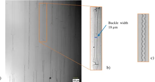
straight-sided buckles into telephone cords morphologies was observed. The occurrence of telephone cords during unloading is commonly seen, as reported by Moon (2004) and is consistent with stability diagram of unilateral buckling patterns established by Parry (2006).Concomitance of buckling and cracking (Figure 6) during testing can be explained with hypothesis on mechanisms of their initiations. It is assumed that given sufficient energy, initiation of buckling, followed by its widening, seems to be the logical sequence of events. However, in areas where adhesion is stronger, buckle enlargement seems more difficult than growth of buckle height. This is likely to generate important bending curvatures that eventually lead to cracking. Therefore, we can formulate the hypothesis that occurrence of buckle or cracking can give information on adhesion at a very local level. Ratio of buckles to cracks populations was estimated to be approximately 2 over an observation area of 1.7 x 2.3 mm².
Figure 6: (a) Concomitance of buckles and cracks observed on SiO2 Type B, (b) measurement of a buckle width, (c) example of a telephone cord associated to the unloading of sample
As for SiO2 Type A, observation of buckle morphologies was hindered by inhomogeneous strain of substrate. Higher compressive stress was indeed needed to see emergence of buckles. At this strain level, polycarbonate substrate is well past softening point, causing strain localization and making results difficult to analyze. This behavior conforms with smaller compressive intrinsic stress being unfavorable to generation of buckles.
3.2.2. Identification of delaminated area
Identification of layer that buckles has been made on a specimen where telephone cords have been removed by tape, in order to release the interface. Step height of delaminated areas, identified with AFM, was found to be 200 nm which corresponds to thickness of SiO2. Profile analysis of chemical composition over a delaminated area shows increased quantity of silicon and oxygen and decreased quantity of carbon on higher zones (Figure 7). These analyses strongly suggest delamination at the SiO2 / Hardcoat interface and support validation of micro-compressive testing as an effective adhesion test to solicit interface of interest.
3.2.3. Quantification of adhesion
Half-width of uncracked buckles averaged over 15 measurements is b = 18±2 µm, using ImageJ software.
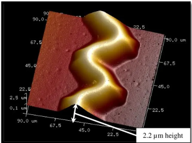
Height of telephone cord observed in post-mortem specimen was estimated to be 2.2 µm by AFM (Figure 8). The
measured height after unloading is underestimate which results in a minimization of calculated energy release rate according to equation (8). This gives values of energy release rates ranging from 2.7 J/m² to 8.9 J/m². This underestimated fracture energy is in the same order of magnitude as bulk fracture resistance of SiO2, between 5 and 8 J/m² as reported by Litteken (2003), which could suggest contribution of plastic energy. Calculated energy release rates are within the range of adhesion energies found in the literature by Xue (2014), for example, 0.8 to 1.2 J/m² for Au on PI and 6.5 J/m² for ITO on Acrylite™.
a)
b)
c) Buckle width
18 µm
Figure 8: AFM characterization of a telephone cord obtained after unloading
Conclusion
Elastic moduli of SiO2 Type A and B were determined by nano-indentation, giving results ranging between 46
and 58 GPa for Si wafer substrate and 14 and 17 GPa for polymeric lens substrate. Same measurements were carried out using AFM. Moduli found are 48 and 64 GPa for Si wafer substrate and 22 and 23 GPa for polymeric lens substrate. Modulus of SiO2 Type B was found to be roughly 20% higher than SiO2 Type A, by nano-indentation. Regarding the high standard deviation of moduli measured by AFM, no significant difference
between elastic moduli of SiO2 Type A and B was observed by AFM on both substrates. However, an important
difference between moduli of SiO2 on lens and on Si wafer was observed. This exposes unexpected influence of substrate on mechanical measurements using AFM, which has been hypothetically attributed to impact of Peak Force high frequency oscillations on viscoelastic substrates. Step height of delaminated areas measured by AFM along with EDS profiles over delaminated area obtained after micro-compressive tests, strongly suggest that delamination occurred at the interface of interest. This gives values of energy release rates ranging from 2.7 J/m² to 8.9 J/m², depending on moduli values found on wafer or lens substrate. Despite wide variation range, values are compatible with bibliographical results. Broader perspectives consist of simulating the micro-compressive adhesion test. Simulation is indeed the only method known to access information such as plastic dissipation or local strain, allowing better analysis of fracture energies.
Acknowledgments
Financial support for the conduct of this research was provided by Essilor International. The authors would like to acknowledge P. Calba’s Materials Advanced Characterization team at Essilor International for their technical support. The authors are also grateful to Bruker’s Nano-Surface Division team for performing characterization of moduli by AFM, using PF-QNM on Dimension Icon.
References
Abdallah A., Kozodaev D., (2006). Buckle morphology of compressed inorganic thin layers on a polymer substrate. Thin Solid Films, 503(1–2),
Amendola, E., Cammarano A., Acierno, D., (2008). A Study of Adhesion of Silicon Dioxide on Polymeric Substrates for Optoelectronic Applications. Optoelectronic Devices and Properties.
Cleymand F., Coupeau C., (2002). Atomic force microscopy investigation of buckling patterns of nickel thin films on polycarbonate substrates. Philosophical Magazine Letters, 82(9), 477–482.
Cordill M. J., Glushko O., Kreith J., (2014). Measuring electro-mechanical properties of thin films on polymer substrates. Microelectronic Engineering, 137, 96–100.
Coupeau C., Naud J. F., Cleymand F., Goudeau P., (1999). Atomic force microscopy of in situ deformed nickel thin films. Thin Solid Films, 353(1), 194–200.
Derjaguin V., Muller V. M. and Toporov P., (1975). Effect of Contact Deformations on the Adhesion of Particles, Journal of Colloid and Interface Science, 53 2 314–326.
Fanchon J., (2016). Guide des sciences et technologies industrielles, Éd. Nathan, ISBN 2091647144
Fang W., Lee C., Hu H., (1999). On the buckling behavior of micromachined beams. Journal of Micromechanics and Microengineering, 9(3), 236–244.
Fateh R., Dillert R., Bahnemann D., (2013). Preparation and characterization of transparent hydrophilic photocatalytic TiO2/SiO2 thin films on polycarbonate. Langmuir, 29(11), 3730–3739.
Hay J., & Crawford, B. (2011). Measuring substrate-independent modulus of thin films. Journal of Materials Research, 26(06), 727-738.
Hopf J., & Pierce, E. M. (2014). Topography and mechanical property mapping of International Simple Glass surfaces with atomic force microscopy. Procedia Materials Science, 7, 216-222.
Jia, Haikun, et al. (2013) "Investigation of buckling transition from straight-sided to telephone-cord wrinkles in Al films." Journal of Micromechanics and Microengineering 23.4 045014.
Leterrier Y., Andersons J., Pitton Y., (1997). Adhesion of silicon oxide layers on poly (ethylene terephthalate). II: Effect of coating thickness on adhesive and cohesive strengths. Journal of Polymer Science Part B: Polymer Physics, 35(9), 1463–1472.
Li H., & Vlassak, J. J. (2009). Determining the elastic modulus and hardness of an ultra-thin film on a substrate using nanoindentation. Journal of Materials Research, 24(03), 1114-1126.
Lian Y., Leu K., Liao S., Tsai W., (1995). Effects of surface treatments and deposition conditions on the adhesion of silicon dioxide thin film on polymethylmethacrylate, 71, 142–150.
Litteken C., Dauskardt R., (2003). Adhesion of polymer thin-films and patterned lines. International Journal of Fracture, 119/120(4–2), 475–485.
Mittal K.L., (1995). Adhesion measurement of films and coatings: a commentary, in K.L. Mittal (Eds.), Adhesion measurement of films and coatings, 1–13.
Moon M-W., et al. (2004) "Buckle delamination on patterned substrates." Acta Materialia 52.10, 3151-3159 Nicu L., Temple-Boyer P., Bergaud C., (1999). Energy study of buckled micromachined beams for thin-film
stress measurements applied to SiO2. Journal of Micromechanics and Microengineering, 9(4), 414–421. Oliver W.C., Pharr G.M., (1992). Improved technique for determining hardness and elastic modulus using load
and displacement sensing indentation experiments, Journal of Materials Research, 7 6 1564-1583.
Parry G., Cimetière A., Coupeau C., (2006). Stability diagram of unilateral buckling patterns of strip-delaminated films. Physical Review E - Statistical, Nonlinear, and Soft Matter Physics, 74(6).
Roisin P., (2012) Method for producing an optical article coated with an antireflection or a reflective coating having improved adhesion and abrasion resistance properties, US 8318245 B2
Scherer K., (1996). Optical and mechanical characterization of evaporated SiO2 layers. Long-term evolution, Applied Optics, 35 25, 5067 – 5072.
Stoney G., (1909). The tension of metallic films deposited by electrolysis, Proceedings of The Royal Society A: Mathematical, Physical and Engineering Sciences, 82 553, 172-175.
Tadanaga, K., Iwashita K., (1996). Coating and Water Permeation Properties of SiOz Thin Films Prepared by the Sol-Gel Method on Nylon-6 Substrates, 11, 107–111.
Trtik P., Kaufmann J., Volz U., (2012). Peak-force tapping atomic force microscopy for quantification of the local elastic modulus in hardened cement paste, Cem. Concr. Res., (42) 1 pp. 215–221.
Xue X., Wang S., Jia H., (2014) Buckling delamination and cracking of thin titanium films under compression: Experimental and numerical studies, Surface and Coatings Technology, 244, 151-157.