Open Archive TOULOUSE Archive Ouverte (OATAO)
OATAO is an open access repository that collects the work of Toulouse researchers and
makes it freely available over the web where possible.
This is an author-deposited version published in :
http://oatao.univ-toulouse.fr/
Eprints ID : 15714
To link to this article : DOI : 10.1016/j.jelechem.2016.03.045
URL :
http://dx.doi.org/10.1016/j.jelechem.2016.03.045
To cite this version :
Assaud, Loïc and Massonnet, Nicolas and
Evrard, David and Vergnes, Hugues and Salvagnac, Ludovic and
Conédéra, Véronique and Noé, Laure and Monthioux, Marc and
Gros, Pierre and Temple-Boyer, Pierre and Caussat, Brigitte A new
route for the integration of a graphene/diazonium/PEDOT
electrode towards antioxidant biomarker detection. (2016) Journal
of Electroanalytical Chemistry, vol. 771. pp. 73-79. ISSN
1572-6657
Any correspondence concerning this service should be sent to the repository
administrator:
[email protected]
A new route for the integration of a graphene/diazonium/PEDOT
electrode towards antioxidant biomarker detection
Loïc Assaud
a,b,⁎
, Nicolas Massonnet
a,b, David Evrard
a, Hugues Vergnes
a, Ludovic Salvagnac
b,
Véronique Conédéra
b, Laure Noé
c, Marc Monthioux
c, Pierre Gros
a, Pierre Temple-Boyer
b, Brigitte Caussat
a,⁎⁎
aLaboratoire de Génie Chimique, Université de Toulouse, CNRS, INPT, UPS, Toulouse, France bLAAS-CNRS, Université de Toulouse, CNRS, Toulouse, France
cCentre d'Elaboration de Matériaux et d'Etudes Structurales, UPR 8011 CNRS, Université Toulouse III, 29 rue Jeanne Marvig, F-31055 Toulouse, France
a b s t r a c t
A new route for the integration of a graphene-based electrode on a silicon substrate was studied for the simulta-neous detection and assay of ascorbic (AA) and uric (UA) acids. Graphene was synthesized by catalytic chemical vapour deposition (CVD) from methane as carbon feedstock onto both platinum foils and supported thin platinum films on silicon wafers which were used as catalyst. Graphene was characterized by Raman spectroscopy and electron microscopies. The resulting electrodes were further functionalized by successive electrodeposition of a stabilizing diazonium layer and a poly(3,4-ethylenedioxythiophene) (PEDOT) conductive film. AA and UA determi-nation on such modified electrode was performed either by cyclic voltammetry or by differential pulse voltammetry. In the latter case, the selectivity was about 380 mV and the sensitivity was 2.40 and 2.75 μA cm−2μM−1for AA and
UA, respectively. The present study shows that monolayer graphene allows a greater sensitivity of AA and UA detec-tion than that observed with modified glassy carbon electrode.
Keywords:
Graphene CVD
Cyclic voltammetry Differential pulse voltammetry Diazonium
PEDOT Uric acid Ascorbic acid
1. Introduction
Oxidative stress results from an imbalance between the production of highly oxidizing species and the antioxidant defense system of human body[1]. Particular attention has been paid to this biochemical process over the last two decades[2,3], mainly because of its presumed implication in early stages of pathologies such as cataract, cancer, cardiovascular and neurodegenerative diseases[4–10]. The antioxidant defense system is composed of a set of enzymes and low molecular weight compounds. Among the latter, ascorbic (AA) and uric (UA) acids are of particular interest. Indeed AA is one of the most powerful hydrophilic antioxidant whereas UA concentration in serum is presum-ably a major marker of specific diseases that may induce heart or kidney problems[11,12]. Moreover, both AA and UA are present in numerous biological fluids (plasma, serum, urine, tears) and are therefore reliable biochemical markers for the detection of the above-mentioned pathol-ogies. Numerous methods exist to quantify AA and UA in body fluids,
in particular enzymatic methods[13], spectrofluorometry[14], high-performance liquid chromatography (HPLC) analysis[15], or capillary electrophoresis[16], but they are expensive and time-consuming. Elec-trochemical sensors[17]could represent a suitable alternative due to their advantages such as low cost, fast analysis and reliability[18–20]. Sensors' performances, namely sensitivity, selectivity, limit of detection and lifetime, can be drastically improved by the functionalization of the electrode surface. In this way, the potentialities of electrografted diazo-nium salts have been studied in recent works since they combine a strong covalent bonding with the electrode surface and a good versatil-ity for further functionalization[21–24]. In particular, the additional electropolymerization of 3,4-ethylenedioxythiophene (EDOT) has proved to be an efficient way to enhance the selectivity of the electrodes
[21,25,26]. Several electrode materials have been considered in previ-ous works such as glassy carbon[21]or gold[27]. Carbon-based elec-trodes are particularly well-suited in terms of versatility and cost-effectiveness: in particular, glassy carbon has shown an exceptionally good behavior for such applications[20,22,26,27]. However, this mate-rial is hardly compatible with the silicon technologies required for a cost-effective mass production in series of integrated microelectrodes and the associated electrochemical microcells[28,29]. On the other hand, graphene is a two-dimensional carbon structure which is used in a growing number of applications because of its high electrical con-ductivity, large specific surface area and excellent electrochemical
⁎ Correspondence to: L. Assaud, ICMMO-ERIEE, Université Paris-Sud, CNRS, rue du Doyen Georges Poitou, F-91400 Orsay, France.
⁎⁎ Corresponding author.
E-mail addresses:[email protected](L. Assaud),[email protected]
(B. Caussat).
stability[30]. It can be produced at reduced costs with a good quality by the catalytic chemical vapour deposition (CVD) process, thus being compatible with silicon technologies[30]. Moreover, graphene has shown high performances in electroanalysis and electrochemical detec-tion of small molecular targets such as hydrogen peroxide or glucose, and nucleic acids[31,32]. Platinum is a good catalyst for graphene synthesis because of the low carbon solubility in Pt (0.005 wt%) close to the deposition temperature (1000 °C)[34], leading to mono-layer graphene. In particular, crystalline graphene mono-layers can be syn-thesized by catalytic CVD on platinum foils[33–36]. Moreover, the high melting point, low thermal expansion coefficient and high inertness of Pt provide a smooth graphene morphology. Lastly, after annealing Pt over 600 °C, the (111) orientation dominates, thus inducing very weak graphene-substrate interactions. Consequently platinum has a quite lim-ited effect on the physical properties of graphene. It has even been shown that the electronic structure of the graphene grown on Pt is nearly the same as that of the free-standing graphene[33]. On another hand, Pt is a well-known conductive material and has been thoroughly used for the fabrication of microelectrodes[37,38]. Furthermore it is fully compat-ible with silicon microtechnologies.
The present study constitutes the first step for the conception of a mass production of microsensors for AA and UA assay. It aims at devel-oping the proof-of-concept of a mixed 4-thiophenylbenzene diazonium (TBD)/poly(3,4-ethylenedioxythiophene) (PEDOT) functionalized graphene electrode integrated on silicon substrate for the simultaneous detection and assay of UA and AA. The protocol of CVD graphene synthesis on (i) Pt foils and (ii) Pt thin films, were first presented, together with the electrochemical functionalization by both TBD salt grafting and EDOT electropolymerization. The Raman spectroscopy, scan-ning electron microscopy (SEM) and transmission electron microscopy (TEM) analyses of the resulting modified electrodes were detailed. Both selectivity and sensitivity for AA and UA oxidations were finally evaluated by electrochemical methods.
2. Experimental
2.1. Chemicals
All products were used as received. Reactive gases for the CVD processes (Ar alpha 1, H2alpha 1 and CH4N45) were supplied either by
Air Liquide or Linde. 4-thio(phen-2-yl)aniline (TPA) (C10H9NS),
3,4-ethylenedioxythiophene (EDOT) (C6H6O2S), sodium nitrite (NaNO2),
tetrabutylammonium hexafluorophosphate (Bu4NPF6), ascorbic acid
(AA) (C6H8O6, 99% powder) and uric acid (UA) (C5H4N4O3, 99% powder)
were purchased from Sigma-Aldrich. Potassium dihydrogenophosphate (KH2PO4), di-potassium hydrogenophosphate (K2PHO4) and acetonitrile
(ACN) (extra dry) were supplied by Acros Organics. Phosphate buffer saline (PBS) solution (0.1 mol L−1, pH 7) was prepared by mixing
dipotassium phosphate and monopotassium phosphate in Milli-Q water (18 MΩ cm). Acid solutions were prepared by dilution of 37% hydrochlo-ric acid (HCl) from VWR using Milli-Q water.
2.2. Catalytic substrates
The graphene synthesis process was first developed using 100-μm thick Pt foils (from Mateck, 99% in purity). In order to demonstrate the feasibility of microelectrodes production in series, Si(100)/SiO2/Ta/Pt
stacks were fabricated from oxidized silicon wafers with a SiO2
thick-ness of 600 nm. Thin metallic layers (10 nm Ta, 100 nm Pt) were depos-ited by sputtering in a conventional UNIVEX 450D physical vapor deposition (PVD) reactor. Tantalum was used as both an adhesion and a barrier layer for Pt on SiO2considering the high temperature required
by the subsequent graphene deposition process. All experiments were conducted with samples of 2 × 2 cm2.
2.3. Chemical vapour deposition
The catalytic CVD of graphene was achieved in a home-made CVD reactor consisting in a horizontal cylindrical quartz tube of 1000 mm length and 90 mm inner diameter, cooled at each extremity by water cir-culation. A gas injection/pumping system enabled the circulation of reac-tive gases and the extraction of unreacted species and by-products. A 760-mm long furnace composed by three heating zones surrounded the tube. Quartz sample-holders were used to maintain the samples in the reactor. The catalytic substrates were placed in the central isothermal part of the heating zone. The full description of the home-made reactor is provided as Supplementary materials Fig. S1 (see e.g.[39]). Graphene was obtained through three successive steps under low pressure Ar/H2reductive
atmosphere (850 and 50 standard cubic centimeters per minute (sccm) respectively). The first step was a thermal pretreatment of the catalytic surface: the substrate was heated from 25 to 1045 °C under low pressure (2.1 Torr) and maintained at 1045 °C for 15 min. The second step consisted in increasing the pressure up to 700 Torr and in introducing 5 sccm of methane (carbon precursor). CH4flow and heating were turned
off after either 12 or 24 min. Finally the substrate was cooled down from 1045 to 25 °C at about 10 °C min−1.
2.4. Graphene characterization
Raman spectroscopy was performed using a HORIBA Jobin Yvon's LabRAM 800HR spectrometer with a 532-nm wavelength laser source.
Scanning electron microscopy analyses were performed using a JEOL 7600 microscope equipped with an Oxford Link ISIS 300 EDX analyzer. Transmission electron microscopy and diffraction were carried out using a CM30 Philips TEM equipped with a LaB6-gun and operated at
150 kV while taking care of limiting electron damaging. The TEM spec-imens were prepared as follows: the graphene layer was protected by a spin coated 500-nm PMMA film. Then H2was bubbled between the
graphene layer and the Pt host substrate by applying a 2 mA current in a 1 M NaOH solution, according to a previously reported procedure
[33,40]. The sample was subsequently transferred to a TEM copper grid (200 mesh) coated with amorphous lacey carbon film allowing for its observation. Note that regarding the graphene synthesized on Pt thin films, the insulating SiO2interlayer did not allow to take a
good electrical backside contact for applying the current, rendering the transfer of graphene delicate. Therefore, only graphene synthesized on Pt foils was characterized by TEM.
2.5. Electrochemical instrumentation
All the electrochemical experiments were performed at room tem-perature using a Metrohm μ−Autolab II potentiostat interfaced to a personal computer and controlled with GPES 4.9 software package. A conventional three-electrode cell was used with a Pt wire and an Ag/AgCl/KCl (3 M) (E°= +0.21 V vs. NHE) electrode connected to the cell by a capillary as counter and reference electrodes, respectively. All the potentials are expressed with respect to this reference. The working electrode was either the unmodified or modified graphene electrode. The working electrodes were either a 5.5 mm-diameter disk (A = 23.8 mm2) or a 1 × 1 cm2square (A = 1.0 cm2) for Pt foil and Pt thin
film electrodes, respectively.
2.6. Electrochemical functionalization of the graphene electrode
Unless otherwise stated, the solutions were deaerated prior to be used by nitrogen during 10 min. Prior to each modification step, the graphene electrode was cautiously washed with Milli-Q water and eth-anol. 4-thiophenylbenzene diazonium (TBD) was prepared according to the following procedure. A cold solution of NaNO2(0.94 mg, 13.9 mmol)
in Milli-Q water (1 mL) was slowly added to a 4 mL ice-cold solution of 0.1 M HCl containing TPA (2.19 mg, 12.4 mmol). The mixture was left to
react at 4 °C for 10 min and then transferred into the electrochemical cell. Diazonium grafting onto graphene was achieved using cyclic volt-ammetry (CV) by recording 10 scans between 0.6 V and −0.4 V at 100 mV s−1.
Poly(3,4-ethylenedioxythiophene) (PEDOT) was generated by recording 10 cyclic voltammograms (CVs) between 0.8 V and 1.5 V at 50 mV s−1in a 0.1 M Bu
4NPF6acetonitrile solution containing 2.5 mM
EDOT. The parameters used were those defined and optimized in a pre-viously reported work from our group[21]. After each modification step, the electrode was carefully rinsed with Milli-Q water and ethanol in order to remove weakly adsorbed moieties.
2.7. Electrochemical detection of ascorbic and uric acids
The electrochemical detection of AA and UA on the functionalized graphene electrode was investigated in 0.1 M PBS solution (pH 7) con-taining an equimolar mixed solution of 200 μM AA and UA by cycling voltammetry and differential pulsed voltammetry at a scan rate of 50 mV s−1. In the former case the potential range used was between
−0.2 V and 0.6 V. In the latter case the potential range used was between −0.2 V and 0.5 V and the following optimized parameters were used for the waveform: modulation time: 0.01 s; interval time: 0.1 s; modulation amplitude: 0.05 V; step potential: 0.005 V.
3. Results and discussion
The steps used to fabricate the graphene-based electrode are sum-marized inFig. 1.
3.1. Synthesis of graphene by chemical vapour deposition
Preliminary CVD experiments were conducted on 100-μm thick Pt-foils in order to obtain high quality graphene. The optimized synthe-sis parameters were temperature, methane concentration, pressure and deposition duration. Once the best synthesis conditions were deter-mined on Pt foils (see theExperimentalsection for detail), these param-eters were applied for graphene synthesis on Ta/Pt thin films. The resulting graphene was characterized again in order to ascertain the good quality of the layer for these experimental conditions.
Fig. 2shows SEM micrographs of graphene flakes obtained on both Pt foils (Fig. 2a,b) and Pt thin films (Fig. 2c,d) using the same synthesis
parameters (12 min of deposition, 5 sccm of methane). Note that it was observed that for a CH4flow rate higher than 5 sccm, graphite
agglom-erates covered the sample surface. OnFig. 2a,b large flakes of 0.03 mm2
and smaller ones of about 25 μm2were observed. A hexagonal shape,
characteristic of monocrystalline graphene, was clearly visible for the smaller ones. OnFig. 2c,d graphene flakes of different sizes close to each other were observed over the entire surface of the thin platinum film. They form an almost continuous graphene-like layer of several cm2
over the entire surface of the thin platinum films. The contrast variation between the flakes was due to the difference of graphene number of layers. Moreover bright and drop-shaped areas underneath the graphene layered were also noticed, as a consequence of a slight dewetting of the Pt layer due to the high CVD process temperature. Pre-liminary experiments carried out using Ti as an adhesion layer instead of Ta led to a total dewetting of the Pt layer (see Supplementary mate-rials Fig. S2), probably because of the high temperature treatment com-bined with the reductive H2atmosphere in the reactor. Thus, the Ta
layer was effective to stabilize the Pt layer.
Fig. 3displays the Raman spectra of graphene deposited during 12 (Fig. 3a) and 24 min (Fig. 3b) on Pt foils and during 12 min on Pt thin films (Fig. 3c). For each surface, analyses were performed on at least six different areas in order to allow a statistical evaluation of the graphene quality. These analyses confirmed that graphene was contin-uous on all the samples.
Raman spectroscopy is commonly used to validate the presence of graphene, as well as to characterize both its structural quality and the number of graphene monolayers. Several features of the resulting spec-tra are well-known to be considered for this purpose (e.g. see Supple-mentary materials S3), in particular considering the different band intensities noted ID, IG, and I2Drespectively[41,42].
Fig. 3shows that each sample presented the characteristic D and G bands of graphenic carbons, and an intense band in the frequency range of the characteristic 2D band. It has to be noted that for the spectra of
Fig. 3a and b, the peak located in the 2D band region (~2700 cm−1)
pre-sents one or two shoulders and exhibits shifts (of 100 cm−1and 50 cm−1
onFig. 3a and b, respectively) towards higher wave numbers for graphene synthesized on Pt foils. This phenomenon is not totally elucidat-ed but it could be assignelucidat-ed to C−H stretching modes or to constraints present in the graphene layer[43]. The 12-minute synthesis on Pt thick foil (Fig. 3a) led to a multi-layer graphene with defects (ID
IG ¼ 0:57),
Fig. 1.Schematic of the graphene-based electrode elaboration and functionalization consisting in four successive steps: i) deposition of a thin Pt film onto a Si(100)/SiO2/Ta
wafer, ii) synthesis of graphene by catalytic chemical vapour deposition, iii) diazonium electrografting and iv) EDOT electropolymerization.
Fig. 2.SEM micrographs of graphene flakes synthesized by catalytic chemical vapor deposition on (a,b) a 100-μm thick Pt foil and on (c,d) a 100-nm Ta/Pt thin film deposited on a Si/SiO2wafer.
whereas increasing the deposition duration up to 24 min on the same substrate (Fig. 3b) and in the same temperature and methane partial pressure conditions led to graphene multi-layer with lower defect con-centration (ID
IG ¼ 0:21). Thus, increasing the graphene CVD duration
in-duced a higher number of graphene layers according to a lower I2D/IG
ratio, but with lower defect concentration. This result is in good agree-ment with those of Lee and Jeong[36]. Our aim in increasing the deposi-tion duradeposi-tion was to reduce the defect concentradeposi-tion by annealing effect and by substrate surface modification, which seems to be verified. The most often assumed mechanism of graphene formation involves a disso-lution of carbon into the metal and a segregation of carbon on the metal surface during the cooling step[33]. According to the work by Lee and Jeong[36], a mechanism of graphene formation by surface adsorption could also co-exist, thus explaining that the number of graphene layers in-creased with the deposition duration.
Since Pt thin films are smoother than Pt foils, the 12-minute long CVD process was chosen for the synthesis of graphene on thin Pt films. The graphene surface obtained (Fig. 3c) presented a very low D band intensi-ty. The corresponding ratio of band intensitiesID
IGwas equal to 0.1 which
corresponded to a low defect concentration, whereas theI2D
IG is equal to
2.45 with a sharp and symmetric 2D band, which corresponds to mono-layer graphene. Furthermore, the full width at half maximum (FWHM)
of the G band was particularly low, confirming the high quality of graphene. Additionally, the FWHM of the 2D band was evaluated for sev-eral measurements performed on different points over the substrate sur-face (inset inFig. 3c). It was close to 31 cm−1which could correspond to
monolayer graphene in turbostratic packing stacking. The low deviation (b10%) of the FWHM values for the several points assessed the uniformi-ty of the graphene layer over the substrate in term of number of layers
[44]. The graphene quality in terms of layer number and defects was thus better on Pt thin films than on Pt foils. This can be explained by the fact that the Pt foils present a non-negligible intrinsic surface rough-ness whereas the Pt films formed by PVD are very smooth.
To further characterize the graphene quality, the samples were ana-lyzed by transmission electron microscopy (TEM).Fig. 4displays the resulting micrographs and diffraction patterns. Low magnification im-ages (Fig. 4a) confirmed that graphene was continuous over large area domains. The domains exhibited wrinkles that probably originated from the deposition process on the TEM grid. Thanks to the wrinkles, high-resolution images (Fig. 4b) showed that the domains were actually not mono-layered graphene but multi-layered graphene, since they were made of less than 10 stacked graphene (a maximum of 5 in the figure) with good nanotexture (i.e., distortions are little). Finally, the diffraction patterns (Fig. 4c) exhibited two sets of six sharp spots con-centrically dispatched according to a hexagonal symmetry, which is the mark of either single-layer graphene or single graphite crystal, when lying flat. As the graphene here were multi-layered (Fig. 4b), the single graphite nature was ascertained (i.e., all the graphene in the stack were coherently piled up according to the ABAB Bernal sequence), at least in the dimension range (~1μm) of the opening of the selection aperture used for obtaining the diffraction patterns[42]. In addition, the spot sharpness was consistent with large, micron-size mono-domains. Note that the transferring step of graphene to the TEM grid could imply a relaxation of constraints. To summarize, the TEM investi-gation showed that the graphene domains grown on Pt foil for 12 mi-nutes were high quality graphene stacked by less than ten layers as micron-sized single graphite crystals.
3.2. Graphene electrode functionalization
The functionalization of the graphene-based electrode was performed by diazonium electrografting followed by EDOT electropolymerization in
Fig. 3.Raman spectra of graphene synthesized by catalytic chemical vapour deposition (a,b) on a 100-μm thick Pt foil and (c) on 100-nm Pt thin film deposited on a Si(100)/ SiO2/Ta wafer. The CVD duration was 12 min (a,c) and 24 min (b). Inset of (c): FWHM
of the 2D band at different locations over the substrate for the graphene layer synthesized on Pt thin film.
Fig. 4.(a) TEM micrograph (plane view) of a free-standing graphene sheet synthesized by catalytic chemical vapour deposition on a Pt foil for a 12-min deposition process, (b) HRTEM cross-section view (wrinkle) of a multi-layered graphene sheet, (c) electron diffraction pattern obtained from a single, multi-layered graphene flake in an area free of wrinkles, hence showing the graphite structure (see text).
a coupled approach (Fig. 1). Graphene electrodes elaborated either on Pt foils or on Pt thin films supported on oxidized Si wafers were investigated. In order to evaluate the graphene stability under the electrochemical conditions, 50 consecutive CVs were first recorded in a 0.1 M PBS (pH 7) solution.Fig. 5a displays the 1st, 25th and last of 50 consecutive scans monitored on a graphene electrode supported on a Pt thin film on oxi-dized wafer. The resulting CVs showed a classical shape with a reduction peak at 0.05 V corresponding to O2reduction and the typical H2
evolu-tion around −0.6 V. The system exhibited a stable behavior as a funcevolu-tion of time since no evolution of the CVs was noticed between the 1st and the 50th scan. Note that the same experiment was conducted on graphene electrode supported on Cu substrates (not shown). In this case, an ohmic contribution increasing with the number of scans was observed. This was attributed to the oxidation and poisoning of the Cu electrode surface by adsorption of reaction by-products, leading to a lower conductivity.Fig. 5b,c show CVs recorded in a 0.1 M HCl solution containing 2.5 mM TBD on Pt foil/graphene and Pt thin film/graphene electrodes, respectively. On the former electrode (Fig. 5b), a cathodic peak located at −0.15 V was observed, which corresponded to the dia-zonium reduction and subsequent grafting onto the graphene surface. It has to be noticed that the typical reduction peak decay and cathodic shift were very progressive all along the 10 consecutive scans, indicating a slow grafting kinetics probably due to the graphene flatness. Con-versely, on the Pt thin film/graphene electrode (Fig. 5c), the self-inhibiting behavior of the grafted organic layer was observed from the second scan, suggesting a faster grafting kinetics in this latter case. Moreover, a reduction pre-peak was noticed around 0.06 V together with the reduction peak at −0.15 V, in accordance with a diazonium reduction process easier on the Pt thin film/graphene than on the Pt foil/graphene. However and except in the case of 4-nitrobenzene diazo-nium[22], the exact mechanism involved in the appearance of this pre-peak remains unclear. The graphene electrodes modified by diazonium grafting were further functionalized by 3,4-ethylenedioxythiophene (EDOT) electropolymerization via cyclic voltammetry.Fig. 5d shows the 1st, 5th and 10th corresponding scans. In accordance with a previously reported work performed on GC electrodes, the monomer oxidation started around 1.3 V and the corresponding current increased all along the electropolymerization process as the result of the polymer formation and subsequent increase of the active surface area[21].
3.3. Biomarker detection
The diazonium/PEDOT functionalized graphene-based electrode was used for the simultaneous detection of uric and ascorbic acids.
Fig. 6presents CVs recorded in a 0.1 M PBS solution (pH 7) containing a 200-μM mixed AA and UA solution.Fig. 6a displays the three succes-sive scans performed on a Pt foil/graphene/diazonium/PEDOT electrode. The two anodic peaks observed on the forward scan and located at 0.05 and 0.4 V were assigned to AA and UA oxidation, respectively. The shapes of these peaks were consistent with a diffusion-controlled pro-cess for AA and an adsorption-limited one for UA, in accordance with previous studies[21,45]. However, it has to be noticed that both peaks exhibited a slightly resistive behavior which was not observed on glassy carbon (GC) material[21]. The peak separation was about 350 mV, demonstrating the high selectivity of the electrode towards the two an-alytical targets. As a comparison, GC modified electrode obtained using the same mixed surface functionalization methods (i.e. TBD and EDOT deposited by cyclic voltammetry, seeSection 2.6) exhibited an analyti-cal response very similar to that of bare GC with an oxidation peak at 0.6 V assigned to UA coupled with a shoulder around 0.25 V assigned to AA[21–Fig. 2]. No real peak separation between UA and AA was ob-served in these two former cases. This observation comforts graphene as a good alternative to GC (modified or not) in terms of selectivity and sensitivity towards AA and UA. Additionally, a recent review[46]
has reported that modified glassy carbon electrodes usually exhibit a AA−UA peak separation around 0.14−0.21 V, whereas using graphene
as interlayer systematically leads to a peak separation higher than 0.2 V. In the present study, the peak separation was in the range of 0.35 V. This evidences the excellent ability of our electrode to improve the selective detection of AA and UA, and further support the enhancement of the electroanalytical response due the graphene interlayer. Furthermore, it has to be noticed that the mixed diazonium/PEDOT interface has proved to be much more stable than PEDOT without diazonium[21]. However, a rapid decrease in the amperometric responses was observed here after three successive scans, since AA oxidation peak current decreased from
Fig. 5.(a) CVs recorded on a Pt thin film/graphene electrode in a 0.1 M PBS (pH 7) solution. The 1st, 25th and 50th cycles are shown. Scan rate: 50 mV s−1. CVs recorded in a 0.1 M HCl
solution containing 2.5 mM TBD (b) on Pt foil/graphene and (c) on Pt thin film/graphene electrodes. Scan rate: 100 mV s−1. (d) CVs recorded in a 0.1 M Bu
4NPF6ACN solution
containing 2.5 mM EDOT on a Pt thin film/graphene electrode previously functionalized by diazonium grafting. The 1st, 5th and 10th cycles are shown. Scan rate: 50 mV s−1.
150 to 40 μA cm−2(73% loss) and UA one decreased from 250 to
90 μA cm−2(64% loss). Although by-products coming from the AA
and UA oxidation could inhibit the detection sites of the electrode, the reason for this phenomenon is not clearly understood yet. However it was not observed on GC electrode. One may then assume that the Pt foil/graphene interface induced a different structuration of the organic layer, altering the conduction properties of the PEDOT film upon cy-cling that led to such a peculiar behavior. Note that the selectivity of the electrode for the simultaneous detection of UA and AA remained unchanged over the scans while peak currents decreased. Similar experiments were carried out on the Si/Pt thin film/graphene/di-azonium/PEDOT electrode supported on oxidized Si wafer (Fig. 6b). In this latter case, AA and UA peaks were slightly better separated (ca. 380 mV), and the resistive behavior noticed on the Pt foil/ graphene/diazonium/PEDOT electrode was no longer observed. These observations supported the assumption of a beneficial structuration of the diazonium layer on the Si/Pt thin film/graphene leading to an en-hanced conductivity and to a better sensitivity of the electrode. Moreover the amperometric response was much more stable upon cycling on the Si/ Pt thin film/graphene/diazonium/PEDOT electrode since the decrease in peak current after the 3 consecutive scans was only b1% and 6% for AA and UA, respectively. Thus, the use of the Pt thin film as graphene substrate afforded a quite good structuration of the electrode functionalization, this latter being suitable for selective and repeatable AA and UA detection. This could play an important role in PEDOT nanostructuration leading to a signal enhancement as compared to GC modified electrode and a higher AA−UA peak separation. This results also in a favorable electron transfer kinetics and electrocatalytic activity toward the oxidation of AA and UA of our graphene/diazonium/PEDOT modified electrode (Fig. 6) again as compared to the GC electrode func-tionalized in the same conditions[21].
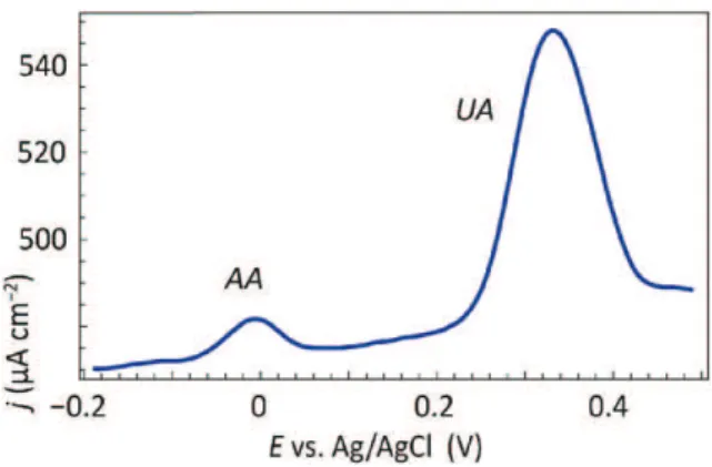
In order to further improve the sensitivity of the modified electrode, measurements were recorded in a AA and UA mixture solution by differ-ential pulsed voltammetry (DPV) using the Si/Pt thin film/graphene/dia-zonium/PEDOT electrode.Fig. 7shows the simultaneous detection
of UA and AA. In this case, the sensitivity for AA detection was about 2.40 μA cm−2 μM−1 at a potential of −5 mV whereas it
reached 2.75 μA cm−2μM−1 for UA detection at a potential of
380 mV again enhanced with respect to GC/diazonium/PEDOT elec-trodes. In optimized conditions, this latter exhibited a sensitivity of 0.665 and 0.345 μA cm−2μM−1for AA and UA, respectively[21]. This
shows again the high sensitivity and selectivity of the graphene-based electrode. It has to be noted that the sensitivity measurements reported in[21]were performed by linear regression for various AA/UA ratios (see e.g.[46]for a quite exhaustive review of the different types of elec-trodes and functionalization methods for AA/UA detection and their performances).
4. Conclusions
In this work, we described the entire process for the synthesis of a graphene-based electrode on thin Pt films deposited on oxidized Si wafer in order to further develop a low cost integrated micro-device produced in series. The results showed that optimized graphene was obtained for a CVD process of 12 min at 700 Torr and 1045 °C. The graphene electrode was then functionalized by a stabilizing diazo-nium layer coupled to a conductive PEDOT layer that confers improved selectivity to the electrode. The resulting electrode was tested for the si-multaneous detection of AA and UA. A high sensitivity of 2.40 and 2.75 μA cm−2μM−1was obtained for AA and UA respectively and the
se-lectivity was about 380 mV. This measurement was performed for an equimolar mixed solution of 200 μM AA and UA. This value was close to that obtained on classical GC electrode. We thus demonstrated the proof-of-concept for the feasibility of fabricating an integrated graphene-based electrode as a basis for future selective and sensitive sensor dedicated to biomarkers. Current works focus on the integration of this electrode into a final micro-device.
Acknowledgements
The authors gratefully acknowledge M. Molinier, E. Prévot and M. De Solan Bethmale (LGC) for their precious technical assistance and the LAAS technological team supported by the French RENATECH network. Dr. Pascal Puech (CEMES) is acknowledged for fruitful discussion on Raman spectra. L. Assaud and N. Massonnet postdoctoral fellowships were granted by FERMAT, Université de Toulouse, CNRS-INPT-UPS-INSA (FR 3089 INPT).
Appendix A. Supplementary data
Supporting information is available from the Wiley Online Library or from the author. Supplementary data associated with this article can be
Fig. 7.Differential pulsed voltammograms of simultaneous UA and AA detection on a functionalized Si/Pt thin film/graphene/diazonium/PEDOT electrode. A 200-μM mixed solution of UA and AA was used. Scanning rate: 50 mV s−1.
Fig. 6.Successive cycles of a CV recorded on a functionalized (a) Pt foil/graphene/ diazonium/PEDOT electrode and (b) Si/Pt thin film/graphene/diazonium/PEDOT electrode in a 0.1 mol L−1, pH 7 PBS solution containing 200 μM mixed AA and UA.
found in the online version, athttp://dx.doi.org/10.1016/j.jelechem. 2016.03.045.
References
[1] G.W. Felton, in: S. Ahmad (Ed.), Oxidative Stress and Antioxidant Defenses in Biol-ogy, Springer, US 1995, p. 356.
[2] E. Cadenas, K.J. Davies, Mitochondrial free radical generation, oxidative stress, and aging, Free Radic. Biol. Med. 29 (2000) 222–230, http://dx.doi.org/10.1016/S0891-5849(00)00317-8.
[3] T. Finkel, N.J. Holbrook, Oxidants, oxidative stress and the biology of ageing, Nature 408 (2000) 239–247,http://dx.doi.org/10.1038/35041687.
[4] M.H. Shishehbor, M.-L. Brennan, X. Fu, M. Goormastic, G.L. Pearce, N. Gokce, J.F. Keaney, M.S. Penn, D.L. Sprecher, J.A. Vita, S.L. Hazen, Association of nitrotyrosine levels with cardiovascular disease and modulation by statin therapy, JAMA 289 (2003) 1675–1680,http://dx.doi.org/10.1001/jama.289.13.1675.
[5] L.M. Sayre, G. Perry, M.A. Smith, Oxidative stress and neurotoxicity, Chem. Res. Toxicol. 21 (2008) 172–188,http://dx.doi.org/10.1021/tx700210j.
[6] I.M. Fearon, G. Phillips, T. Carr, M. Taylor, D. Breheny, S.P. Faux, The role of oxidative stress in smoking-related diseases, Mini-Rev. Org. Chem. 8 (2011) 360–371,http:// dx.doi.org/10.2174/157019311797440317.
[7] H. Tohgi, T. Abe, K. Yamazaki, T. Murata, E. Ishizaki, C. Isobe, Alterations of 3-nitrotyrosine concentration in the cerebrospinal fluid during aging and in patients with Alzheimer's disease, Neurosci. Lett. 269 (1999) 52–54,http://dx.doi.org/10. 1016/S0304-3940(99)00406-1.
[8] T.J. Anderson, Nitric oxide, atherosclerosis and the clinical relevance of endo-thelial dysfunction, Heart Fail. Rev. 8 (2003) 71–86,http://dx.doi.org/10. 1023/A:1022199021949.
[9] R.F. Loeser, C.S. Carlson, M. Del Carlo, A. Cole, Detection of nitrotyrosine in aging and osteoarthritic cartilage: correlation of oxidative damage with the presence of interleukin-1β and with chondrocyte resistance to insulin-like growth factor 1, Ar-thritis Rheum. 46 (2002) 2349–2357,http://dx.doi.org/10.1002/art.10496. [10] G.T. Liberatore, V. Jackson-Lewis, S. Vukosavic, A.S. Mandir, M. Vila, W.G. McAuliffe,
V.L. Dawson, T.M. Dawson, S. Przedborski, Inducible nitric oxide synthase stimulates dopaminergic neurodegeneration in the MPTP model of Parkinson disease, Nat. Med. 5 (1999) 1403–1409,http://dx.doi.org/10.1038/70978.
[11] G.C. Curhan, E.N. Taylor, 24-h uric acid excretion and the risk of kidney stones, Kidney Int. 73 (2008) 489–496,http://dx.doi.org/10.1038/sj.ki.5002708. [12] D.I. Feig, D.-H. Kang, R.J. Johnson, Medical progress: uric acid and cardiovascular risk,
N. Engl. J. Med. 359 (2008) 1811–1821,http://dx.doi.org/10.1056/NEJMra0800885. [13] Y. Zhao, X. Yang, W. Lu, H. Liao, F. Liao, Uricase based methods for determination of uric acid in serum, Microchim. Acta 164 (2009) 1–6,http://dx.doi.org/10.1007/ s00604-008-0044-z.
[14] S. Feng, J. Wang, X. Chen, J. Fan, Kinetic spectrofluorimetric determination of trace ascorbic acid based on its inhibition on the oxidation of pyronine Y by nitrite, Spectrochim. Acta A Mol. Biomol. Spectrosc. 61 (2005) 841–844,http://dx.doi.org/ 10.1016/j.saa.2004.06.008.
[15]K.R. Dhariwal, W.O. Hartzell, M. Levine, Ascorbic acid and dehydroascorbic acid measurements in human plasma and serum, Am. J. Clin. Nutr. 54 (1991) 712–716 (doi: ajcn.nutrition.org/content/54/4/712.abstract).
[16] Y. Tao, X. Zhang, J. Wang, X. Wang, N. Yang, Simultaneous determination of cysteine, ascorbic acid and uric acid by capillary electrophoresis with electrochemiluminescence, J. Electroanal. Chem. 674 (2012) 65–70,http://dx.doi.org/10.1016/j.jelechem. 2012.03.009.
[17] C. Amatore, S. Arbault, in: A.C. Michael, L. Borland (Eds.), Electrochemical Methods for Neuroscience, CRC Press, Boca Raton 2006, p. 544.
[18] V.B. Koman, C. Santschi, N.R. von Moos, V.I. Slaveykova, O.J.F. Martin, Portable oxida-tive stress sensor: dynamic and non-invasive measurements of extracellular H2O2
released by algae, Biosens. Bioelectron. 68 (2015) 245–252,http://dx.doi.org/10. 1016/j.bios.2014.12.044.
[19] T.-H. Tsai, T.-W. Chen, S.-M. Chen, Selective electroanalysis of ascorbic acid using a nickel hexacyanoferrate and poly(3,4-ethylenedioxythiophene) hybrid film modi-fied electrode, Electroanalysis 22 (2010) 1655–1662,http://dx.doi.org/10.1002/ elan.200900610.
[20] Y. Li, X. Lin, Simultaneous electroanalysis of dopamine, ascorbic acid and uric acid by poly (vinyl alcohol) covalently modified glassy carbon electrode, Sensors Actuators B Chem. 115 (2006) 134–139,http://dx.doi.org/10.1016/j.snb.2005.08.022. [21] W. Richard, D. Evrard, P. Gros, A novel electrochemical sensor based on a mixed
di-azonium/PEDOT surface functionalization for the simultaneous assay of ascorbic and uric acids. Towards an improvement in amperometric response stability, Electro-analysis 26 (2014) 1390–1399,http://dx.doi.org/10.1002/elan.201300632. [22] W. Richard, D. Evrard, P. Gros, New insight into 4-nitrobenzene diazonium
reduc-tion process: evidence for a grafting step distinct from NO2electrochemical
reactiv-ity, J. Electroanal. Chem. 685 (2012) 109–115,http://dx.doi.org/10.1016/j.jelechem. 2012.09.014.
[23] D.-J. Chung, K.-C. Kim, S.-H. Choi, Electrochemical DNA biosensor based on avidin– biotin conjugation for influenza virus (type A) detection, Appl. Surf. Sci. 257 (2011) 9390–9396,http://dx.doi.org/10.1016/j.apsusc.2011.06.015.
[24] S.M. Khor, G. Liu, J.R. Peterson, S.G. Iyengar, J.J. Gooding, An electrochemical immunobiosensor for direct detection of veterinary drug residues in undiluted com-plex matrices, Electroanalysis 23 (2011) 1797–1804,http://dx.doi.org/10.1002/ elan.201100205.
[25] V.S. Vasantha, S.-M. Chen, Electrocatalysis and simultaneous detection of dopa-mine and ascorbic acid using poly(3,4-ethylenedioxy)thiophene film modified
electrodes, J. Electroanal. Chem. 592 (2006) 77–87,http://dx.doi.org/10.1016/ j.jelechem.2006.04.026.
[26] A. Balamurugan, S.-M. Chen, Poly(3,4-ethylenedioxythiophene-co-(5-amino-2-naphthalenesulfonic acid)) (PEDOT-PANS) film modified glassy carbon electrode for selective detection of dopamine in the presence of ascorbic acid and uric acid, Anal. Chim. Acta 596 (2007) 92–98,http://dx.doi.org/10.1016/j.aca.2007.05.064. [27] F. Sékli Belaïdi, P. Temple-Boyer, P. Gros, Voltammetric microsensor using
PEDOT-modified gold electrode for the simultaneous assay of ascorbic and uric acids, J. Electroanal. Chem. 647 (2010) 159–168,http://dx.doi.org/10.1016/j.jelechem. 2010.06.007.
[28] C. Christophe, F. Sékli Belaïdi, J. Launay, P. Gros, E. Questel, P. Temple-Boyer, Elaboration of integrated microelectrodes for the detection of antioxidant species, Sensors Actua-tors B Chem. 177 (2013) 350–356,http://dx.doi.org/10.1016/j.snb.2012.11.032. [29] D. Aguilar, C. Barus, W. Giraud, E. Calas, E. Vanhove, A. Laborde, J. Launay, P.
Temple-Boyer, N. Striebig, M. Armengaud, V. Garçon, Silicon-based electrochemical microdevices for silicate detection in seawater, Sensors Actuators B Chem. 211 (2015) 116–124,http://dx.doi.org/10.1016/j.snb.2015.01.066.
[30] A.C. Ferrari, F. Bonaccorso, V. Fal’ko, K.S. Novoselov, S. Roche, P. Bøggild, S. Borini, F.H.L. Koppens, V. Palermo, N. Pugno, J.A. Garrido, R. Sordan, A. Bianco, L. Ballerini, M. Prato, E. Lidorikis, J. Kivioja, C. Marinelli, T. Ryhänen, A. Morpurgo, J.N. Coleman, V. Nicolosi, L. Colombo, A. Fert, M. Garcia-Hernandez, A. Bachtold, G.F. Schneider, F. Guinea, C. Dekker, M. Barbone, Z. Sun, C. Galiotis, A.N. Grigorenko, G. Konstantatos, A. Kis, M. Katsnelson, L. Vandersypen, A. Loiseau, V. Morandi, D. Neumaier, E. Treossi, V. Pellegrini, M. Polini, A. Tredicucci, G.M. Williams, B. Hee Hong, J.-H. Ahn, J. Min Kim, H. Zirath, B.J. van Wees, H. van der Zant, L. Occhipinti, A. Di Matteo, I.A. Kinloch, T. Seyller, E. Quesnel, X. Feng, K. Teo, N. Rupesinghe, P. Hakonen, S.R.T. Neil, Q. Tannock, T. Löfwander, J. Kinaret, Science and technology roadmap for graphene, related two-dimensional crystals, and hybrid systems, Nanoscale 7 (2015) 4598–4810,http://dx.doi.org/10.1039/C4NR01600A. [31] Y. Liu, X. Dong, P. Chen, Biological and chemical sensors based on graphene materials,
Chem. Soc. Rev. 41 (2012) 2283–2307,http://dx.doi.org/10.1039/C1CS15270J. [32] J. Liu, Z. Liu, C.J. Barrow, W. Yang, Molecularly engineered graphene surfaces for
sensing applications: a review, Anal. Chim. Acta 859 (2015) 1–19,http://dx.doi. org/10.1016/j.aca.2014.07.031.
[33] L. Gao, W. Ren, H. Xu, L. Jin, Z. Wang, T. Ma, L.-P. Ma, Q. Fu, L.M. Peng, X. Bao, H.M. Cheng, Repeated growth and bubbling transfer of graphene with millimetre-size single-crystal grains using platinum, Nat. Commun. 3 (2012) 699-1–699-7,http://dx.doi.org/10. 1038/ncomms1702.
[34] B.J. Kang, J.H. Mun, C.Y. Hwang, B.J. Cho, Monolayer graphene growth on sputtered thin film platinum, J. Appl. Phys. 106 (2009) 104309,http://dx.doi.org/10.1063/ 1.3254193.
[35] Y. Li, X. Wu, H. Wu, H. Qiang, Redistribution of carbon atoms in Pt substrate for high quality monolayer graphene synthesis, J. Semicond. 36 (2015) 013005-1–013005-6 (doi: stacks.iop.org/1674-4926/36/i=1/a=013005).
[36] B.J. Lee, G.H. Jeong, Comparative study on graphene growth mechanism using Ni films, Ni/Mo sheets, and Pt substrates, Appl. Phys. A Mater. Sci. Process. 116 (2014) 15–24,http://dx.doi.org/10.1007/s00339-014-8493-1.
[37] P.M. Tatauliker, D.A. Price, J.J. Burmeister, S. Nagari, J.E. Quintero, F. Pomerleau, P. Huettl, J.T. Hastings, G.A. Gerhart, Ceramic-based microelectrode arrays: recording surface characteristics and topographical analysis, J. Neurosci. Methods 198 (2011) 222–229,http://dx.doi.org/10.1016/j.jneumeth.2011.04.004.
[38] L. Assaud, J. Schumacher, A. Tafel, S. Bochmann, S. Christiansen, J. Bachmann, Systematic increase of electrocatalytic turnover at nanoporous platinum surfaces prepared by atomic layer deposition, J. Mater. Chem. A 3 (2015) 8450–8458,
http://dx.doi.org/10.1039/C5TA00205B.
[39] P. Trinsoutrot, C. Rabot, H. Vergnes, A. Delamoreanu, A. Zenasni, B. Caussat, High quality graphene synthesized by atmospheric pressure CVD on copper foil, Surf. Coat. Technol. 230 (2013) 87–92,http://dx.doi.org/10.1016/j.surfcoat.2013.06.050. [40]L. Shi, Y. Liu, F. Yang, L. Gao, J. Sun, A symmetrical bi-electrode electrochemical
technique for high-efficiency transfer of CVD-grown graphene, Nanotechnology 25 (2014) 145704 (doi: stacks.iop.org/0957-4484/25/i=14/a=145704).
[41] A.C. Ferrari, J.C. Meyer, V. Scardaci, C. Casiraghi, M. Lazzeri, F. Mauri, S. Piscanec, D. Jiang, K.S. Novoselov, S. Roth, A.K. Geim, Raman spectrum of graphene and graphene layers, Phys. Rev. Lett. 97 (2006) 187401,http://dx.doi.org/10.1103/PhysRevLett.97. 187401.
[42] H.J. Park, J. Meyer, S. Roth, V. Skakalova, Growth and properties of few-layer graphene prepared by chemical vapor deposition, Carbon 48 (2010) 1088–1094,
http://dx.doi.org/10.1016/j.carbon.2009.11.030.
[43] A.C. Ferrari, J. Robertson, Resonant Raman spectroscopy of disordered, amorphous, and diamondlike carbon, Phys. Rev. B 64 (2001) 075414,http://dx.doi.org/ 10.1103/PhysRevB.64.075414.
[44] Y.Y. Wang, Z.H. Ni, T. Yu, Z.X. Shen, H.M. Wang, Y.H. Wu, W. Chen, A.T.S. Wee, Raman studies of monolayer graphene: the substrate effect, J. Phys. Chem. C 112 (2008) 10637–10640,http://dx.doi.org/10.1021/jp8008404.
[45] F. Sekli Belaidi, A. Civélas, V. Castagnola, A. Tsopela, L. Mazenq, P. Gros, J. Launay, P. Temple-Boyer, PEDOT-modified integrated microelectrodes for the detection of ascorbic acid, dopamine and uric acid, Sensors Actuators B Chem. 214 (2015) 1–9,
http://dx.doi.org/10.1016/j.snb.2015.03.005.
[46] M. Sajid, M.K. Nazal, M. Mansha, A. Alsharaa, S.M. Sajid Jillani, C. Basheer, Chemically modified electrodes for electrochemical detection of dopamine in the presence of uric acid and ascorbic acid: a review, Trends Anal. Chem. 76 (2016) 15–29,http:// dx.doi.org/10.1016/j.trac.2015.09.006.