HAL Id: hal-01868631
https://hal.archives-ouvertes.fr/hal-01868631
Submitted on 5 Sep 2018
HAL is a multi-disciplinary open access
archive for the deposit and dissemination of
sci-entific research documents, whether they are
pub-lished or not. The documents may come from
teaching and research institutions in France or
abroad, or from public or private research centers.
L’archive ouverte pluridisciplinaire HAL, est
destinée au dépôt et à la diffusion de documents
scientifiques de niveau recherche, publiés ou non,
émanant des établissements d’enseignement et de
recherche français ou étrangers, des laboratoires
publics ou privés.
Advanced modulation format using silicon modulators in
the O-band
Diego Perez-Galacho, Laurent Bramerie, Charles Baudot, Mohamed Chaibi,
Sonia Messaoudène, Nathalie Vulliet, Laurent Vivien, Christophe Peucheret,
Delphine Marris-Morini
To cite this version:
Diego Perez-Galacho, Laurent Bramerie, Charles Baudot, Mohamed Chaibi, Sonia Messaoudène, et al..
Advanced modulation format using silicon modulators in the O-band. SPIE Photonics West - OPTO
2018, Jan 2018, San Francisco, CA, United States. pp.105351K, �10.1117/12.2291888�. �hal-01868631�
Advanced modulation format using silicon modulators in the O-band
D. Pérez Galacho
1, L. Bramerie
2, C. Baudot
3, M. Chaibi
2, S. Messaoudène
3, N. Vulliet
3, L. Vivien
1,
C. Peucheret
2, D. Marris-Morini
11
Centre de Nanosciences et de Nanotechnologies, CNRS, Univ. Paris-Sud, Université Paris-Saclay,
C2N-Orsay, 91405 Orsay, France
2
Univ Rennes, CNRS, FOTON – UMR 6082, F-22305 Lannion, France
3ST Microelectronics, 850 rue Jean Monnet, 38920 Crolles, France
ABSTRACT
This paper review our recent work on silicon modulators based on free carrier concentration, working in the O-band of optical communications (1260 nm - 1360 nm) for short distance applications. 25 Gbit/s OOK modulation is obtained using a driving voltage of 3.3 Vpp , and QPSK dual-drive Mach-Zehnder modulator (DDMZM) operating in the O-band is
demonstrated for the first time.
Keywords: silicon modulator, advanced modulation format, QPSK, Mach Zehnder
1. INTRODUCTION
Significant research effort has been dedicated over the past years to the development of silicon-based photonic technologies [1-2]. Developing high performance silicon modulators based on the free-carrier plasma dispersion (FCPD) effect has been an important milestone. These modulators are commonly based on carrier depletion in PN junctions and outstanding performances have already been demonstrated [3-4]. However, in order to keep up with the growing bandwidth demand in datacom applications, it is necessary to move from binary on-off keying (OOK) modulation format to more advanced formats such as 4-level pulse amplitude modulation (PAM-4) or quadrature phase-shift keying (QPSK). Advanced modulation formats using silicon modulators have already been demonstrated [5-8]. However, most of these demonstrations have been carried out in the C-band of optical communication systems (1530 nm - 1570 nm) where the FCPD is stronger. Nevertheless, it is believed that silicon photonics is the best suited for next generation of short range optical fiber communications, where current standards favor the use of the O-band (1260 nm - 1360 nm) in order to exploit the zero-dispersion region of standard single-mode fibers. In this work we present results on high performance silicon modulators operating in the O-band, including efficient OOK modulation and the first demonstration of a QPSK silicon-based dual-drive Mach-Zehnder modulator (DD-MZM) operating in the O-band.
2. SILICON MODULATOR DESIGN
The active region of the Mach Zehnder modulator is illustrated in Fig 1. (a). It is based on a PN diode embedded in a silicon-on-insulator (SOI) waveguide. The waveguide width and eight are 400 nm and 300 nm, respectively, while its slab height is 50 nm. The PN diode is obtained by boron and phosphorus implantation of the waveguide. Targeted doping concentrations are P = 5 × 1017 cm−3 and N = 1.4×1018 cm−3. The junction interface is 25 nm shifted from the center of the
waveguide to benefit from larger effective index variation. Highly doped P++ and N++ regions are used away from the
optical mode to reduce access resistance without increasing optical losses. The modulators were fabricated using the 300 mm DAPHNE technological platform from STMicroelectronics [9].
The phase shifter efficiency was estimated by measuring the transmission of ring resonators embedding the phase shifter inside the ring, as a function of the applied voltage. The results was a Vπ Lπ product between 0.95 Vcm and 1.15 Vcm for
carrier depletion based modulators in the O-Band.
Mach-Zehnder modulators are using a dual drive configuration, as schematically illustrated in Fig 1. (b). Phase shifter lengths of 1 mm or 2 mm have been used in both arms of symmetric Mach-Zehnder structures. Multi-mode interference (MMI) couplers are used as input/output splitter and combiner. Metallic heaters form low speed/high efficiency static phase shifters, in order to tune the direct current (DC) phase shift Φ between both arms. The radio frequency (RF) signals are applied on each PN phase shifter independently, using GSGSG coplanar waveguides, while DC tips are used to apply the static phase shift (Fig 1. (c)).
Figure 1. (a) Phase shifter design: a PN diode is located in the SOI rib waveguide; (b) layout of the dual-drive Mach Zehnder modulator; (c) picture of the device under test.
3. OOK MODULATION
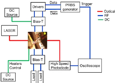
The set-up used for OOK modulation characterization is schematically reported in Fig 2. Both arms of the 1 mm long DD-MZM were driven in push-pull configuration, i.e. one arm is driven with the PRBS data signal and the other with its complementary. The heaters were used to set the interferometer to the quadrature point. Thanks to the push-pull configuration and the high efficiency of the active region, it has been possible to reduce the voltage swing down to 3.3 Vpp,
with a DC bias of 1.7 V. The corresponding eye diagram at 25 Gbps is reported in Fig. 3. An extinction ratio (ER) of 5 dB was obtained, while the total on-chip losses were 3.6 dB at this operating point.
Figure 2. Schematic representation of the set-up used for OOK-modulation characterization.
Figure 3. Measured eye diagram at 25 Gbps of the 1 mm long DD-MZM with an applied voltage swing of 3.3 Vpp and 1.7 V DC bias.
4. QPSK MODULATION
DD-MZMs can also be used to generate QPSK signals with a simpler structure than standard IQ modulators based on nested MZMs [11-12]. Furthermore, this scheme allows a reduction of the driving voltage applied to the transceiver and thus to the power consumption to generate the QPSK constellation, offering a better power efficiency and scalability that
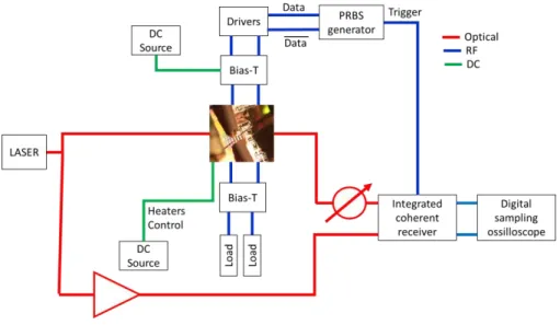
are key advantages for short distance intra data center communications. The set-up used for QPSK modulation characterization at 20 Gbps (10 Gbaud) is reported in Fig 4.
Figure 2. Schematic representation of the set-up used for QPSK-modulation characterization. Two 215−1 long de-correlated
pseudo random binary sequences at 10 Gbps are applied on each of the MZ arm.
Two 215−1 long de-correlated pseudo random binary sequences (PRBSs) at 10 Gbps were amplified to reach a swing
voltage Vpp of 7 V and applied to each of the phase shifters in order to achieve a peak-to-peak phase modulation of π in
each arm, while the phase-shift introduced by the heater is adjusted to operate the DD-MZM at the quadrature point (Φ=π/2). TE-polarized light from an O-band external cavity laser followed by a fiber polarization controller was coupled to the photonic integrated circuit using a single polarization grating coupler (GC). The same laser was also used as local oscillator (LO). The modulated optical signal was then sent to the coherent receiver through a variable optical attenuator in order to adjust the received power. The I/Q signals of the receiver were fed to a 40 Gsps digital sampling oscilloscope (DOS) with 16 GHz electrical bandwidth. Blocks of 105 symbols were acquired and then processed offline. An adaptive
finite impulse response (FIR) filter with decision-directed least mean square (DD-LMS) tracking was used as digital signal processing (DSP). The processed samples were used to obtain the constellation diagrams and to compute bit error rate (BER). The BER was calculated over five blocks of 105 symbols.
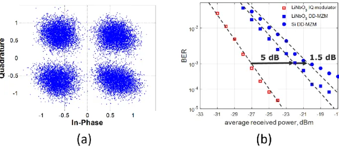
For QPSK modulation characterization, a 2 mm-long MZM was used, as it is necessary to achieve a phase variation on each arm of the MZM. On-chip optical losses are estimated below 3.8 dB, corresponding to 2.6 dB for the 2 mm-long active region, while losses below 0.6 dB are estimated for each MMI couplers. After DSP, a classical QPSK constellation diagram was obtained, as illustrated in Fig 5. (a) for a receiver input power of -22 dBm. The measured BER performance of the Si DD-MZM is reported in Fig 5. (b), and compared with that obtained with a LiNbO3 modulator in a standard IQ
configuration and a LiNbO3 modulator in a DD-MZM configuration. It can be seen that a penalty of 5 dB occurs between
generation scheme. Interestingly the power penalty of the silicon DD-MZM is only 1.5 dB with respect to its LiNbO3
counterpart.
Figure 5. (a). Typical QPSK constellation diagram after DSP of the Si DD-MZM modulator at 10 Gbaud (20 Gbps), (b) Measured BER as a function of the average received power for the Si DD-MZM under investigation, and comparison with LiNbO3 modulator in DD-MZM configuration and LiNbO3 IQ modulator.
5. CONCLUSION
In this paper we reported our recent work on Si modulators working in the O-band, targeting short range communications. The design of high performance silicon modulators is challenging at this wavelength because the free carrier plasma dispersion effect is weaker than in the C-band. However 25 Gbit/s OOK operation is demonstrated using a push pull configuration, with a reduced peak-to-peak voltage of 3.3 V, and on chip optical loss of only 3.6 dB at the operating point. A DD-MZM can also be used to generate QPSK modulated signals. We thus demonstrated for the first time the use of a silicon DD-MZM to generate a QPSK signal in the O-band.
ACKNOWLEDGMENTS
This work was supported by the European project Plat4m (FP7-2012-318178) and the European project Cosmicc (H2020-ICT-27-2015-688516). Support of French Industry Ministry/DGE through the Nano2017 program is also acknowledged.
REFERENCES
[1] Boeuf, F. et al, Silicon Photonics R&D and manufacturing on 300-mm wafer platform, Journal of Lightwave Technology, 34 (2), 286-295 (2016).
[2] Dong, P., et al, Silicon photonic devices and integrated circuits, Nanophotonics 3 (4-5), 215 (2014).
[3] Dong, P. et al, High-speed low-voltage single-drive push-pull silicon Mach-Zehnder modulators, Optics Express, 20 (6), 6163 (2012)
[5] Dong, P, Xie C., Chen L., Buhl LL., Chen Y-K. 112-Gb/s monolithic PDM-QPSK modulator in silicon., Opt Express 2012, 20, B624–9.
[6] Dong P., Liu X., Sethumadhavan C., Buhl LL., Aroca R., Baeyens Y., Chen Y. 224-Gb/s PDM-16-QAM modulator and receiver based on silicon photonic integrated circuits. In Optical Fiber Communication Conference/National Fiber Optic Engineers Conference 2013, (Optical Society of America, 2013), paper PDP5C.6.
[7] Ding, J. et al, Silicon 16-QAM optical modulator driven by four binary electrical signals, Optics Letters 42 (8),1636 (2017)
[8] Samani, A., et al, Experimental parametric study of 128 Gb/s PAM-4 transmission system using a multielectrode silicon photonic Mach Zehnder modulator, Optics Express 25 (12), 13252 (2017).
[9] Baudot, C., Fincato, A., Fowler, D., Perez-Galacho, D., Souhaité, A., Messaoudène, S., Blanc, R., Richard, C., Planchot, J., De-Buttet, C., Orlando, B., Gays, F., Mezzomo, C., Bernard, E., Marris-Morini, D., Vivien, L. , Kopp, C. and Boeuf, F., “Daphne silicon photonics technological platform for research and development on wdm applications,” in “SPIE Photonics Europe,” (International Society for Optics and Photonics, 2016), pp. 98911D– 98911D.
[10] Perez-Galacho, D., et al, Low voltage 25Gbps silicon Mach-Zehnder modulator in the O-band, Optics Express, 25 (10) 11217 (2017).
[11] Ho, K.-P., Cuei, H.-W., Generation of arbitrary quadrature signals using one dual-drive modulator, Journal of Lightwave Technology 23 (2) 764 (2005).
[12] Krause D.J., et al, Demonstration of 20-Gb/s DQPSK with a single dual-drive Mach–Zehnder modulator, IEEE Photonics Technology Letters, 20 (6), 1363 (2008).