HAL Id: hal-02434571
https://hal.archives-ouvertes.fr/hal-02434571
Submitted on 10 Jan 2020
HAL is a multi-disciplinary open access
archive for the deposit and dissemination of
sci-entific research documents, whether they are
pub-lished or not. The documents may come from
teaching and research institutions in France or
abroad, or from public or private research centers.
L’archive ouverte pluridisciplinaire HAL, est
destinée au dépôt et à la diffusion de documents
scientifiques de niveau recherche, publiés ou non,
émanant des établissements d’enseignement et de
recherche français ou étrangers, des laboratoires
publics ou privés.
Band Phased Array Antennas
Aurélien Ayissi Manga, Raphaël Gillard, Renaud Loison, Isabelle
Leroy-Naneix, Christian Renard
To cite this version:
Aurélien Ayissi Manga, Raphaël Gillard, Renaud Loison, Isabelle Leroy-Naneix, Christian Renard.
Experimental Validation of a Correcting Coupling Mechanism to Extend the Scanning Range of
Nar-row Band Phased Array Antennas. IEEE Transactions on Antennas and Propagation, Institute of
Electrical and Electronics Engineers, 2020, 68 (3), pp.2078-2086. �10.1109/TAP.2019.2957079�.
�hal-02434571�
Abstract— This paper presents a technique designed to extend
the scanning range of a probe-fed patch array whose performances are limited by scan blindness, due to a strong surface wave coupling. The current framework relates to the context of radar applications requiring a large scanning range (up to 60°) and where no inter-element spacing modification is possible as a result of strong T/R modules integration constraints. The proposed solution is based on the introduction of an additional correcting coupling within the array, by means of microstrip lines connecting the sources two by two. A thorough step-by-step description of the design methodology is introduced. It is then implemented in the case of a single-polarized 10-element patch array operating in X band. Simulation results as well as an experimental validation of the concept are presented. They assess the effective improvement of the active impedance matching and realized gain resulting from the use of connecting lines.
Index Terms——antenna arrays, coupling, scan blindness,
surface wave, Radar.
I. INTRODUCTION
HEN radiating elements are located close to one another, as it is the case in phased array antennas, parasitic electromagnetic interferences occur between them. The impact of these couplings is usually harmful since it alters the radiating properties and the active input impedance of the sources. Compactness objectives and radioelectric performances required for airborne radars can lead to structures that support and even foster these parasitic couplings, in the form of surface or space waves. For large arrays, mutual coupling can cause the active reflection coefficient of sources to tend toward unity for specific values of scan angle and frequency, thus forbidding any efficient radiation from the array [1]. This phenomenon, referred to as scan blindness, significantly reduces the operational scan volume of a radar system and should therefore be mitigated.
This paragraph of the first footnote will contain the date on which you submitted your paper for review.
A. Ayissi Manga, is with the Institute of Electronics and Telecommunications of Rennes (IETR), 35700 Rennes, France and with Thales Defence Mission Systems, Elancourt, France (e-mail: aurelien.ayissi-manga@fr.thalesgroup.com).
R. Gillard and R. Loison are with the Institute of Electronics and Telecommunications of Rennes (IETR), 35700 Rennes, France.
I. Le Roy-Naneix and C. Renard are with Thales Defence Mission Systems, 78990 Elancourt, France.
Many different techniques to mitigate coupling effects and scan blindness have been reported in the literature since the early developments of phased arrays [2]. Conventional solutions to tackle coupling problems are based on the reduction of electromagnetic interactions between the array sources. They generally consist in using shielding [3] or metamaterial (such as Electromagnetic Band-Gap or Defected Ground Structures) placed between array sources, in the substrate or in a radome [4-5]. However, these solutions generally lead to complicated, large-area structures, or tend to deteriorate gain and front-to-back ratio of the array [6]. Other solutions rely on non-uniform arrays, whose goal is to avoid the constructive recombination of couplings by breaking the array periodicity [7]. In [8] for example, a weighted thinned array of 8 elements with a scanning range of [-60°; 60°] is proposed. However, irregular inter-element spacing may represent an additional technological constraint on the integration of T/R modules in the case this solution is applied to a radar antenna. Using tapered slot antenna arrays such as the Vivaldi presented in [9] is another way to obtain wideband and wide scan angles possibilities but the required 3D configuration is not suitable for the present application where we restrict the investigations to purely planar topologies.
Alternatively, one can also try to obtain a wide scanning range by fostering couplings within the array. That is the case of connected and tightly-coupled antennas arrays, whose goal is to emulate Wheeler’s current sheet in order to provide wide bandwidth and high-scan capabilities antennas. In [10], an infinite array of connected slots loaded with Artificial Dielectric Layers (ADL) is designed and simulated. A scanning range of ±50° is achieved in all azimuth planes within an octave bandwidth (6.5-14.5 GHz). A different approach consists in compensating harmful mutual coupling effects by providing an additional “correcting coupling” mechanism between the elements of a given array. This method involves the introduction of connecting structures, either between feeding circuits of the sources, or between the sources themselves. Conductive strips and shunt components can be exploited to provide currents distributions that are equal in magnitude and in phase opposition with those of the initial coupling wave, hence cancelling the overall coupling. In [11] for example, a decoupling network consisting in transmission lines placed between source feeds of a 1×16 element array reduces the coupling between adjacent sources to lower than -35 dB at the center frequency, allowing the array to scan up to 66°. In [12] and [13], the connection is established directly on the radiating elements themselves,
Experimental Validation of a Correcting
Coupling Mechanism to Extend the Scanning
Range of Narrow-Band Phased Array Antennas
Aurelien Ayissi Manga, Raphael Gillard, Renaud Loison, Isabelle Le Roy-Naneix, Christian Renard
achieved, in the context of MIMO applications.
As mentioned in [1], the patch array investigated in this paper suffers from scan blindness, due to a strong wave coupling within the structure. Present work aims at mitigating the detrimental effect of the initial coupling wave in order to ensure good impedance matching over a scanning range as wide as possible. To do so, we utilize a similar approach to the one used in [12-13], i.e. with the connecting lines at the same level as the patches for lower impact on the feeding network. Nevertheless, our objective is not to improve the decorrelation between elements, as in MIMO systems. We aim at improving the scanning range of the antenna and thus propose an original optimization approach that directly addresses this constraint. Unlike other examples of correcting coupling found in the literature, the solution operates in the context of scan blindness.
This work follows on the study we carried out in [14], where correcting coupling is used to expand the scanning range of a canonical 3-element probe-fed patch array. The goal of the current paper is to assess correcting coupling for larger narrow-band arrays, where the mutual coupling leads to scan blindness, and to give an experimental demonstration. To meet this dual objective, the work presented in this paper is organized as follows. First, the new investigated 10-element array is introduced in Section II. In Section III, an extensive step-by-step description of the proposed design methodology is presented in the general case of an N-element array. Theoretical results obtained in the case of the 10-element array are analyzed in Section IV. Section V completes the study by providing an experimental validation of the concept, through measurement of a prototype array.
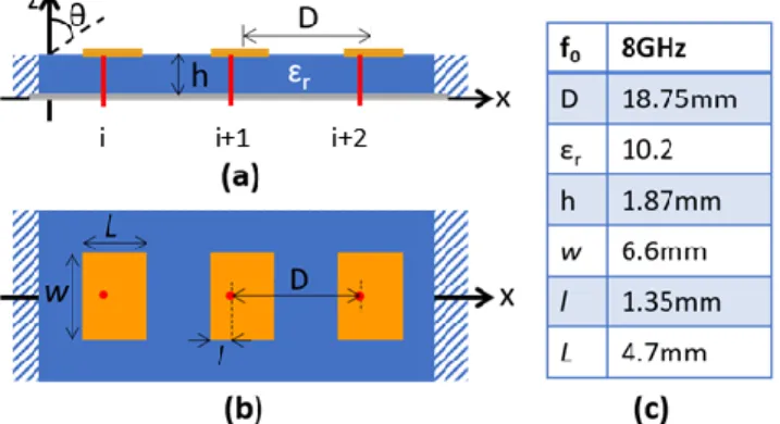
II. INITIAL PERFORMANCES OF THE INVESTIGATED ARRAY The studied antenna (Fig.1) consists of an array of N=10 identical microstrip patches aligned along the x axis, operating at f0 = 8 GHz. The patches (conductivity σ = 59,6×10⁶ S·m-1)
are placed on a substrate of relative permittivity εr = 10.2, loss
tangent tan δ = 0.0023 and height h = 1.87 mm, probe-fed by T/R modules (amplifiers, phase shifters) located below the ground plane. The inter-element spacing is D = 18.75 mm = 0.5λ0 at f0. The scan angle θscan varies in the E-plane (xz-plane).
Fig. 1. Geometry of the studied array: (a) side view (b) top view (c) main characteristics
the fundamental Floquet mode of the corresponding infinite array for a specific scan angle θmax, given by [15]:
θmax = sin-1[(2π/D - βs)/k0] (1)
In this equation, k0 is the free space wave number and βs is
the surface wave phase constant, approximated with [15]: βs = k0 [1+0.5(k0h(1-εr-1)2] (2) For the considered test-case, (1) and (2) yield θmax= 69°.
Fig.2 depicts the module of the active reflection coefficients |Γi| for some sources of the investigated array (simulated using
HFSS®). It is given by: |Γi|= 𝑏𝑖 𝑎𝑖= ∑ |𝑆𝑖𝑗𝑎𝑗| |𝑎𝑖| 𝑁 𝑗=1 (3)
Where 𝑎𝑖 and 𝑏𝑖 are the incoming and outgoing waves at the feed port of the radiating element indexed i.
Fig. 2. Modules of simulated active reflection coefficients |Γi| v. scan
angle θscan
Scan blindness is characterized by a steep increase of |Γi|
when θscan tends toward θmax. It is particularly visible for
low-index sources (i = 1, i = 2, i = 5 in Fig.2), as they are the most affected by couplings when the array scans toward positive θscan [16]. In the following, we define the “blind zone” as the angular range for which |Γi| > -10 dB. As seen in Fig. 2, it
appears around 50°. Note that the maximum value of |Γi| is
observed close to 69°, the theoretical value obtained from (1). A larger array would lead to an even worse mismatch. However, the present 10-element configuration offers a good trade-off: the scan blindness effect is significant enough and the reduced number of elements makes the analysis, as well as the manufacture and test of a full-scale breadboard relatively easy.
To better assess mismatching effects in the 10-element array, two global indicators are used throughout this paper: the averaged and maximum active reflection coefficients, Γavg and
Γmax respectively. They are defined as follows:
𝛤𝑎𝑣𝑔(𝜃𝑠𝑐𝑎𝑛) = 20 𝑙𝑜𝑔10∑ |𝛤𝑖(𝜃𝑠𝑐𝑎𝑛)|
𝑁 𝑖=1
Γ𝑚𝑎𝑥(𝜃𝑠𝑐𝑎𝑛) = max(20 log10|Γ𝑖(𝜃𝑠𝑐𝑎𝑛)|) (5) The solid and dotted red lines in Fig. 6 depict these indicators for the studied array. One can see that the average operational scanning range (on which Γavg < -10 dB) covers
[0°; 51°]. The present goal is to extend this operational scanning range by 10°. This objective directly echoes industrial aspirations, in the context of applications requiring a large scanning range (up to 60°) and where no inter-element spacing modification is possible as a result of strong T/R modules integration constraints.
III. PROPOSED SOLUTION: THE CORRECTING COUPLING
A. Principle
To achieve this objective, the proposed approach consists in connecting sources two by two by means of microstrip lines. The potential of this easy-to-implement approach has already been highlighted in [14]. Adjacent sources are connected on their non-radiating edges, as depicted in Fig.3.
Fig. 3. The proposed correcting coupling implementation By adjusting the dimensions of the connecting lines, it becomes possible to tune the additional coupling generated between the sources. Adjustable parameters include:
1) Lj, the physical length of the connecting line j, which
controls itselectrical length 𝜙j,
2) Wj, the width of the connecting line j, which controls
its characteristic impedance Zj,
3) Pj, the location of the connecting interfaces between
patches and lines.
For the sake of simplicity, the number of variables is limited by using centered connections (Pj = P0 = 0mm). The width of
the lines is also set to a low value (Wj = W0 = 250um). The
choice of this value is not arbitrary, but results from an optimization conducted in the case of a canonical 2-element array. Furthermore, the line narrowness eases the routing between patches and the quite high characteristic impedance (Zj = 105Ω) also prevents from excessively disturbing the
radiation mechanism. B. Theoretical formulation
The optimization of this additional coupling mechanism requires an insightful way to quantify the impact of connecting lines on final array performances. To tune the connecting lines while limiting the resort to time-consuming EM simulations,
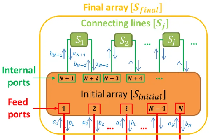
an analytical formulation of the problem is proposed. The S-matrix of the final N-element array (with connecting lines) [Sfinal], can be inferred from the matrices of the initial array
[Sinitial] and from that of the different connecting lines, [Sj].
The process starts with a full-wave simulation of the initial array. In this preliminary simulation, the (N-1) connecting lines are not yet implemented. Instead, in addition to the N feeding ports, we set 2 × (N-1) internal ports on the edges of the patches, at the positions the lines will occupy in the final array (Fig. 4). This yields a (3N-2) × (3N-2) matrix, corresponding to [Sinitial].
Fig. 4. The internal ports of the initial array
On the other hand, each one of the (N-1) connecting lines can be represented by an ideal 2×2 S-matrix:
[𝑆𝑗] = [ 0 𝑒 −𝑗ϕj
𝑒−𝑗ϕj 0 ], (5)
assuming the line is lossless and its characteristic impedance has been used as the reference impedance for internal ports. Note that this step relies on a purely analytical model of the lines and requires no additional EM simulations.
Finally, [Sinitial] and the (N-1) [Sj] can be combined as
shown in Fig. 5. This provides an equivalent circuit for the final array, whose scattering matrix [Sfinal] can be computed
analytically (using Matlab for example).
Fig. 5. Block-diagram relating the initial array, the connecting lines and the final array
subsequently the active reflection coefficients, are dependent on the N-1 electric lengths of the connecting lines, represented by the “N-1-tuple” (1, 2, …,N-1). The active reflection of the source i can be expressed with:
|Γ𝑖(𝜃𝑠𝑐𝑎𝑛)| = ∑
𝑆̃𝑖,𝑛𝑒−𝑗𝑛𝑘0𝐷 sin 𝜃𝑠𝑐𝑎𝑛
𝑒−𝑗𝑖𝑘0𝐷 sin 𝜃𝑠𝑐𝑎𝑛
𝑁
𝑛=1 (6)
Where 𝑆̃𝑖,𝑛 are the parameters of [Sfinal]. This analytical
methodology allows both saving time and automating the final array optimization, regardless of its size, as will be shown in the next section.
C. Optimization process
The optimization of the connecting lines is carried out using a Matlab-developed tool. This program inputs the matrix of the initial array [Sinitial] and outputs (N-1) connecting lines
allowing the expansion of the initial operational scanning range. The code explores the space solution by comparing the different N-1-tuples (ϕ1, … , ϕN−1) by means of a cost function
F. F is defined as the sum of samples of all N active reflection coefficients over a desired angular range:
𝐹 = ∑𝑁𝑖=1∑𝑀𝑚=1|𝛤𝑖(𝜃𝑚)| (7)
where M is the number of angular samples θj.
The optimization, whose goal is to minimize F, is also constrained by the impedance matching condition, to be respected for every sample θj:
|𝛤𝑖(𝜃𝑗)| < −10 𝑑𝐵 (8)
This inequality ensures that recovering impedance matching for high scan angles will not deteriorate the performances for low scan angles. Looking at the expressions (7) and (8), it clearly appears that the proposed correcting coupling approach does not aim at cancelling mutual coupling between sources, but rather at improving impedance matching of the array on a more global scale. Exploration of the solution space is conducted in two stages:
1) N-1-tuples are first processed using a Random Brute Force Search (RBFS) algorithm, to swap away local minima.
2) After a certain number of random iterations, a native Matlab solver (fmincon) based on the Gradient algorithm is used to progress more finely toward the optimum value.
IV. IMPLEMENTATION OF THE ANALYTICAL METHOD IN THE 10-ELEMENT ARRAY
A. Analytical optimization (Matlab)
The proposed methodology is now applied to the 10-element case-study. In the present situation, the optimization consists in 700,000 iterations of RBFS algorithm, followed by 14 iterations of Matlab fmincon solver. Fig. 6 shows the
converting electrical lengths 𝜙j to physical lengths 𝐿𝑗 such
that 𝐿𝑗 > 𝐷, so that the connection between two sources is
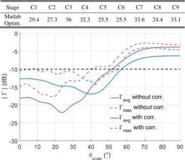
feasible). Compared to the initial array (without correction), the operational scanning range of the final array (with correction) is extended by 7°, and now covers [0°; 58°]. The improvement of Γmax is quite significant and the performances strongly tend toward the set objective.
Fig. 6. Analytical performances of the array (Γmax and Γavg v. θscan,
Matlab)
One can notice that to optimize performances in the high scan region, the algorithm deteriorates impedance matching in the low scan region, but |Γn| remains inferior to -10 dB for all
sources (Fig.6). In that respect, these first results are rather encouraging. Besides, given the fact that the Matlab optimization only takes 8 mins (a third of the time required to simulate a single design with HFSS, for a given reference computer) the benefit of the proposed methodology becomes manifest.
B. Final validation (HFSS) 1) Impedance matching characteristics
The red curves in Fig. 7 represent the performances of the optimized array (with connecting lines) when it is modeled on HFSS. In comparison with Fig. 6, the Γmax curve highlights a
strong deterioration of impedance matching in the low scan region (imputable to source 9). Since the Matlab optimization routine is based on an analytical (and thus ideal) modeling of the connecting lines, it only yields theoretical results. To take into account all the effects due to the implementation of real microstrip lines (discontinuities and couplings), a post-optimization stage can be conducted using a full-wave simulation tool. This additional stage is not time-consuming since the initial Matlab-optimization provides a good starting point and guarantees a very fast convergence. The
TABLEI
LENGTHS OF THE OPTIMIZED CONNECTING LINES IN MM
Stage C1 C2 C3 C4 C5 C6 C7 C8 C9 Matlab
performances of the final array obtained after this post-optimization stage are represented by the blue curves in Fig. 7 (HFSS simulation), while Table 2 gives the lengths of the corresponding connecting lines.
Fig. 7. Performances of the array with correction before and after post-optimization (HFSS)
We see that not only is the impedance matching restored for low scan angles, but the post-optimization process also appears to take advantage of additional physical effects to expand the scanning range even more. The lengths of the connecting lines vary only little between the Matlab optimization and the HFSS validation.
2) Radiation characteristics
Fig.8 represents the evolution of the realized gain as a function of the scan angle, for the simulated array, with and without correcting coupling.
Fig. 8. Evolution of the realized gain as a function of θscan for the
arrays with and without correction (HFSS)
This graph validates the favorable impact of the enhanced impedance matching on the realized gain level. The
improvement brought by the connecting lines is particularly visible for θscan > 47°, a scan angle that corresponds to the onset of the initial blind zone. Compared with the array without correction, the gain is improved by more than 4 dB for θscan = 60°. Conversely for θscan < 47°, the realized gain of the initial array is slightly higher than that of the final one. This is a consequence of the better impedance matching obtained with the initial array for low scan angles on one hand, and of stronger losses in the final array (due to the electrically thin connecting lines) on the other hand. Indeed, the radiation efficiency falls from 96% in the initial array to 90% in the final one.
The radiation patterns depicted in Fig. 9 provide information about the directivity and co- and cross-polarization levels according to Ludwig’s third definition [16].
Fig. 9. Directivity patterns of the arrays in co- and cross-polar: (a) E-plane (θscan = 0°) (b) H-plane (θscan = 0°) (c) E-plane (θscan = 52°)
TABLE2
LENGTHS OF THE OPTIMIZED CONNECTING LINES IN MM
Stage C1 C2 C3 C4 C5 C6 C7 C8 C9 Matlab
Optim. 29.4 27.3 36 32.3 25.5 25.5 33.6 24.4 33.1 HFSS
remains at least 20 dB below co-polarization in the scanning direction, it is not considered to be a blocking factor for the targeted applications. Besides, no critical rise of cross-polarization levels is observed elsewhere in space. Nevertheless, further work has been conducted and a new geometry of connecting line has been proposed to reduce the level of cross-polarization in [17]. This solution consists in connecting adjacent patches on their opposite sides rather than on the same side (as shown in Figure 10). It has been successfully implemented in the case of 1×50 and 3×50 arrays in [17], allowing to extend the scanning range by 10° and 8° respectively, while using identical microstrip lines between all the radiating elements.
Fig. 10. The additional correcting mechanism introduced in [17]
C. Frequency analysis
Fig. 11 represents the evolution of the realized gain for 3 values of scan angle (0°, 40° and 50°) on the [7.5 GHz - 8.5 GHz] frequency range. The phase law is re-calculated for every frequency (true-time phase delay). Depending on the scan angle, the impact of the correcting coupling on the frequency bandwidth is different:
1) For θscan = 0°, the realized gain of the final array is not as good as that of the original one at f0, but an
(unexpected) increase of 0.5dB on both sides of f0 can
be observed. In this case, the strongly narrow-band behavior of the initial array may explain why the comparison is more favorable to the array with correction.
2) For θscan = 40°, the case without correction exhibits better performances at f0. This is not surprising as
improvement is expected only after 47° (Fig.8). 3) For θscan = 50°, two main observations can be made.
First, the improvement begins before f0 (at 7.8 GHz)
and spreads beyond 8 GHz. Furthermore, this improvement is limited by the entrance of the grating lobe in the visible space. Since D = 0.5λ0, any
increase of the frequency goes with a drop in realized gain level of at least 3 dB, due to the partition of the radiated power between two lobes. This downgrade comes from the geometry of the initial array rather than from the proposed solution. However, it is
entrance of the grating lobe in visible space.
Fig. 11. Evolution of the realized gain as a function of frequency, for the initial (dotted lines) and final (solid lines) arrays (HFSS) V. PROTOTYPING OF THE INVESTIGATED 10-ELEMENT ARRAY
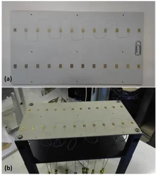
A. Realization
Two arrays (one with connection lines and one without) are printed side by side on a RO6010® substrate of thickness h = 1.905 mm, relative permittivity εr = 10.2, loss tangent δ =
0.0023 and dimensions 120 mm 220 mm (Fig.12 a).
Fig. 12. Manufacturing of the 10-element prototypes with and without connecting lines correction
A distance of 4.5 cm separates the edges of the two circuits (enough to ensure that they do not interfere with each other). The dielectric sheet is fixed on a 3D-printed ABS mechanical structure to facilitate its handling. The probe feeds are implemented with UT-047 semi-rigid coaxial cables (dielectric diameter: 0.94 mm, inner conductor diameter: 0.29 mm), stripped at their extremity and welded on top of the patches (Fig.12 b).
B. S-parameters measurement
Fig. 13 represents the evolution of measured reflection coefficients |Sii| as a function of the frequency, with and
without correction.
Fig. 13. Measured reflection coefficients |Sii| v. frequency,
(a) with correction (b) without correction
One can notice that the resonant frequency f0 of realized
arrays has shifted from 8 GHz to 7.5 GHz. This difference between simulations and measurements is primarily explained by the actual characteristics of the substrate. Firstly, its measured thickness is more important than expected (1.95 mm instead of 1.905 mm). Secondly, retro-simulations suggested its actual dielectric constant is close to 10.6 (instead of 10.2), which is compliant with claimed tolerances for RO6010 material.
Subsequently, some considerations on the way the measurement results have to be interpreted arise from such change in the resonant frequency. In particular, no real scan blindness is expected at 7.5GHz since max is complex in that
case. Nevertheless, the observation of |Γi| on the [7 GHz-8.5
GHz] frequency range already gives insightful indications on the correcting coupling potential and performances. In Fig.13, one can note that the connecting lines do not reduce the individual bandwidths. On the contrary, they often expand it and even lower the minimum levels of |Sii| at f0 (see sources 2,
7 and 9 for example).
C. Active reflection coefficients analysis
The active reflection coefficients |Γi| are now computed as a
function of the scan angle. The beam steering is carried out on Matlab, using the measured S matrices and the following expression [15]:
Γ𝑖(𝜃𝑠𝑐𝑎𝑛) = 𝑒𝑗𝑘.𝑖.𝐷𝑠𝑖𝑛𝜃𝑠𝑐𝑎𝑛∑10𝑚=1𝑆𝑚𝑛𝑒−𝑗𝑘𝑚𝐷𝑠𝑖𝑛𝜃𝑠𝑐𝑎𝑛 (10)
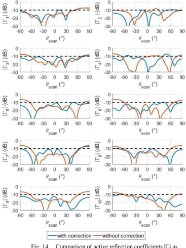
The active reflection coefficients |Γi| are represented in Fig.
14, at 7.5 GHz. Fig. 15 depicts the averaged and maximum active reflection coefficients Γavg and Γmax on [-90°, 90°], with
and without correction.
As mentioned above, no real scan blindness is present at 7.5 GHz. Consequently, the initial averaged operational scanning range is quite large and covers [-67°, 73°]. Indeed, apart from sources 2 and 4, all patches are initially matched on [-60°, 60°]. However, even in this case, the implementation of the connecting lines expands the averaged scanning range and
significantly improves Γmax indicator by enhancing the
scanning performances of sources 2 and 4.
Fig. 14. Comparison of active reflection coefficients |Γi| as
functions of the scan angle, with and without correction
Fig. 15. Evolution of Γavg and Γmax with the scan angle, with and
without correction
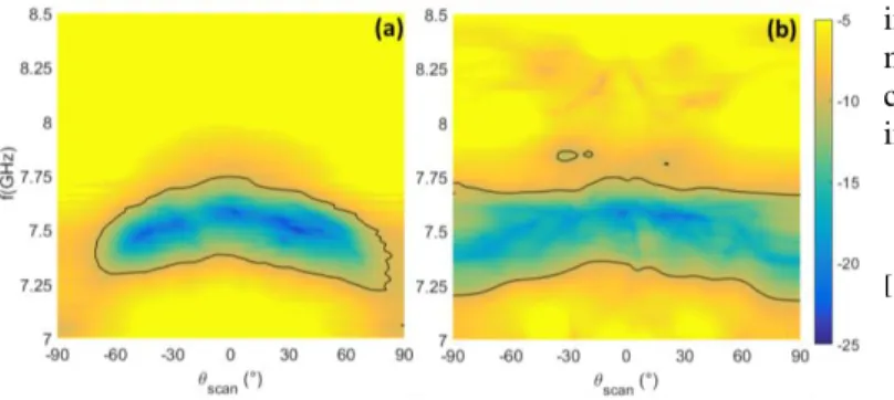
The measured S matrices can also be used to provide a precise mapping of the performance of the two prototyped arrays as functions of both frequency and scan angle (Fig.16).
In this plot, the black contour surrounds the region where Γavg<-10 dB. It shows a clear expansion of the averaged
Fig. 16. Measured Γavg as a function of frequency and scan angle
(a) without correction (b) with correction
In addition, it illustrates the “dilution” phenomenon raised previously: the scanning range is expanded at the expense of a slightly poorer impedance matching for low scan angles. This figure also demonstrates the robustness of performances with respects to frequency. It confirms the results from Section III, as the bandwidth remains quite similar with and without corrections. Finally, within this bandwidth, typically [7.35 GHz-7.68 GHz], the average scanning range is widely expanded and now covers [-90°, 90°]. Thus, although uncertainty on the used dielectric material did not lead to real scan blindness for the initial array, the correcting coupling still demonstrates its capabilities to significantly improve the performance and to meet the objective set up in Section II.
VI. CONCLUSION
This paper presents a solution to extend the scanning range of a narrow-band patch array whose performances are limited by scan blindness. The proposed solution is based on the introduction of an additional correcting coupling within the array, by means of microstrip lines connecting the sources two by two. The potential of this easy-to-implement correcting coupling approach has been highlighted in the literature in the case of MIMO applications. In this instance however, the solution has to operate over a wide scan angle and not only at broadside, and in the context of heavy mutual coupling leading to scan blindness. Hence, it does not try to cancel the initial harmful coupling, but rather helps disturbing its coherent recombination at the scan blindness angle. Consequently, by tuning the electrical lengths of the correcting lines, the active input impedance matching can be improved over the desired scanning range.
Based on an analytical methodology whose purpose is to limit the use of 3D EM simulation, the scanning range of a linear 10-element array suffering from scan blindness is expanded by more than 10°, to cover [0, 65°]. The concept of the proposed solution and its design methodology are then validated experimentally with a prototype of the investigated array. Measurements confirm that by achieving a tradeoff between low and high-scan performances, the correcting coupling approach allows extending the scanning range.
As the solution proposed in this article remains inherently narrow-band, further work should focus on extending its bandwidth (using an approach based on filter synthesis for example), as well as expanding its principle to 2D arrays and dual-polarized antennas. Although not straightforward, a preliminary assessment of this technique to 2D arrays is given
chosen identical due to the reduced finiteness effects, resulting in a greater ease of implementation.
REFERENCES
[1] R. B. Waterhouse, “The use of shorting posts to improve the scanning range of probe- fed microstrip patch phased arrays,” in IEEE Transactions on Antennas and Propagation, vol 44, no. 3, pp. 302-309, Mar 1996.
[2] S. Edelberg, A. Ollvers, "Mutual coupling effects in large antenna arrays: compensation effects", IRE Transactions on Antennas and Propagation, vol 8, no. 4 pp. 360 – 367, 1960
[3] R. Mailloux, “Surface waves and anomalous wave radiation nulls on phased arrays of TEM waveguides with fences”, Transactions on Antennas and Propagation, vol 20, no.2 pp. 160-166, 1972.
[4] P.Rodriguez-Ulibarri, T.Crépin, C.Martel, F.Boust, F.Falcone, C.Loecker, K.Herbets, T.Bertuch, J-P.Martinaud, J-A Marcotegui and M.Beruete, “Experimental demonstration of metamaterials application for mitigating scan blindness in phased array antennas”, EPJ Appl. Metamat, 2013,3,9.
[5] L.Peng, C.I.Ruan and J.Xiong, “Compact EBG for multi-band applications”, ,” in IEEE Transactions on Antennas and Propagation, vol 60, no. 9, pp. 4440-4444, Sept 2012.
[6] E.Rajo-Iglesias, O.Quevedo-Teruel and L.Inclan-Sanchez, “Mutual coupling reduction in patch antenna arrays by using a planar EBG structure and a multilayer dielectric substrate,” in IEEE Transactions on Antennas and Propagation, vol 56, no. 6, pp. 1648- 1655, Jun 2008 [7] R. Mailloux, L. Zahn, A. Martinez, “Grating lobe control in limited scan
arrays”, Transactions on Antennas and Propagation, vol 27, no.1, pp. 79-85, 1979.
[8] Y Bai, S.Xiao,M.Tang,Z.Ding, B.Wang, “Wide-Angle Scanning Phased Array With Pattern Reconfigurable Elements”, IEEE Transactions on Antennas and Propagation,vol 59, no.11, Now 2011.
[9] P.I.Bantavis, C. I.Kolistidas, T.Empliouk,M.L.Roy,B.L.G.Johnson, G.A.Kyriacou, “A Cost-effective Wideband Switched Beam Antenna System for a Small Cell Base Station”, IEEE Transactions on Antennas and Propapation, 2018.
[10] W.Syed, D.Cavallo, H.Shivamurthy, A.Neto, “Wideband, Wide-Scan Planar Array of Connected Slots Loaded With Artificial Dielectric Superstrates”, IEEE Transactions on Antennas and Propagation, vol 64, no.2, pp.543-553, Feb 2016.
[11] R. Xia, S. Qu, P. Li, D. Yang, S.Yang, Z.Nie, “Wide-Angle Scanning Phased Array Using an Efficient Decoupling Network”, IEEE Transactions on Antennas and Propagation,vol 63, no.11, Nov 2015. [12] S.M Amjadi, K. Sarabandi, ”Mutual coupling mitigation in broadband
multiple-antenna communication systems using feedforward technique”, IEEE Transactions on Antennas and Propagation, vol 24, no.5, pp.1642-1652, May 2016.
[13] G.Shaker,G.Rafi, S.Safavi-Naeini, N.Sangary “A Synthesis Technique for Reducing Mutual Coupling Between Closely Separated Patch Antennas”, IEEE Antennas and Propagation Society International Symposium, 2008.
[14] A.Ayissi Manga, R.Gillard, R.Loison, I.Leroy-Naneix, C. Renard, “Implementation of a Correcting Coupling Mechanism to Mitigate Surface Wave in Phased Arrays”, 12th European Conference on
Antennas and Propagation (EUCAP), 2018.
[15] A. K. Bhattacharyya, Phased Array Antennas, John Wiley and Sons, Inc, 2006, pp.104
[16] A.Ayissi Manga, R.Gillard, R.Loison, I.Leroy-Naneix, C. Renard, “A switching mechanism to mitigate scan blindness in phased arrays”, 11th
European Conference on Antennas and Propagation (EUCAP), 2017. [17] A.Ayissi Manga, R.Gillard, R.Loison, I.Leroy-Naneix, C. Renard, “A
Correcting Coupling Solution to Extend the Scanning Range of Large Printed Phased Arrays by Means of Identical Microstrip Lines Connecting the Sources Two by Two”, 13th European Conference on