HAL Id: hal-00698631
https://hal.archives-ouvertes.fr/hal-00698631
Preprint submitted on 18 May 2012
HAL is a multi-disciplinary open access
archive for the deposit and dissemination of
sci-entific research documents, whether they are
pub-lished or not. The documents may come from
teaching and research institutions in France or
abroad, or from public or private research centers.
L’archive ouverte pluridisciplinaire HAL, est
destinée au dépôt et à la diffusion de documents
scientifiques de niveau recherche, publiés ou non,
émanant des établissements d’enseignement et de
recherche français ou étrangers, des laboratoires
publics ou privés.
Electric pulse induced electronic patchwork in the Mott
insulator GaTa4Se8
Vincent Dubost, Tristan Cren, François Debontridder, Dimitri Roditchev, C.
Vaju, V. Guiot, Laurent Cario, Benoît Corraze, Etienne Janod
To cite this version:
Vincent Dubost, Tristan Cren, François Debontridder, Dimitri Roditchev, C. Vaju, et al.. Electric
pulse induced electronic patchwork in the Mott insulator GaTa4Se8. 2012. �hal-00698631�
Vincent Dubost, Tristan Cren, Fran¸cois Debontridder, and Dimitri Roditchev
Institut des Nanosciences de Paris, Universit´e Pierre et Marie Curie, CNRS UMR 7588, 4 place Jussieu, F-75005 Paris, France
Cristian Vaju, Vincent Guiot, Laurent Cario, Benoˆıt Corraze, and Etienne Janod
Institut des Mat´eriaux Jean Rouxel, CNRS Universit´e de Nantes, UMR 6502, 2 rue de la Houssini`ere, BP32229, 44322 Nantes, France
(Dated: May 16, 2012)
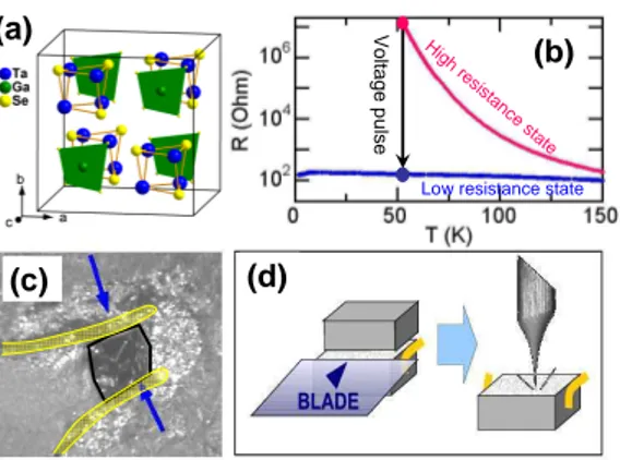
Following a recent discovery of the Insulator-to-Metal Transition induced by electric field in GaTa4Se8, we performed a detailed Scanning Tunneling Microscopy/Spectroscopy study of both pristine (insulating) and transited (conducting) crystals of this narrow gap Mott insulator. The spec-troscopic maps show that pristine samples are spatially homogeneous insulators while the transited samples reveal at nanometer scale a complex electronic pattern that consists of metallic and super-insulating patches immersed in the pristine super-insulating matrix. Surprisingly, both kinds of patches are accompanied by a strong local topographic inflation, thus evidencing for a strong electron-lattice coupling involved in this metal-insulator transition. Finally, using a strong electric field generated across the STM tunneling junction, we demonstrate the possibility to trig the metal-insulator tran-sition locally even at room temperature.
PACS numbers: 74.25.Gz, 74.72.Jt, 75.30.Fv, 75.40.-s
Many correlated materials exhibit exotic properties like metal-insulator transitions (MIT) in transition-metal oxides or chalcogenides, high-Tc superconductivity in cuprates, colossal magnetoresistance in manganites. These phenomena are frequently associated with spatial electronic inhomogeneities or even electronic phase sepa-ration. The presence of patches with different magnetic, metallic or insulating nature was demonstrated in many real-space studies of systems such as manganites [1–3],
cuprates superconductors [4–8], VO2 [9–12], Ca
substi-tuted Sr2RuO4 [13]. Generally, in these systems, the
MIT is induced by tuning either the hopping amplitude via pressure (bandwidth-controlled transition) or band-filling via chemical doping (doping-controlled transition) [16]. In addition to these ways of controlling the elec-tronic state of correlated materials, we recently discov-ered that short electric field pulses could also drive the
MIT in the Mott insulator GaTa4Se8 [17–19]. Such a
new way to electrically induce a MIT might be interest-ing for electronic devices, in particular if this MIT can be controlled at the nanometer scale at room temperature.
The Mott insulator GaTa4Se8adopts a deficient spinel
structure (Fig.1a) of rocksalt-type packing of Ta4Se4
cubanes and GaSe4 tetrahedra [20, 21]. This compound
belongs to a specific class of Mott insulators in which cor-relations do not take place at the atomic scale but rather
at the scale of the Ta4 clusters [22]. This makes these
compounds easier to tune through the Metal-Insulator-Transition as it reduces the magnitude of Coulomb
re-pulsion. GaTa4Se8 is a rare example of stoichiometric
Mott insulator that undergoes a pressure-induced MIT and even a superconductor transition [20]. Recently we
found that an electric field pulse through GaTa4Se8
in-duces a MIT (see Fig.1b), accompanied at low
temper-ature by granular superconductivity [17, 23]. While the microscopic origin of this effect remains undecided, it was experimentally found in [23] that the temperature evolu-tion of the resistance on the metallic side of the MIT in
single crystals of GaTa4Se8 can be accounted for by a
two channel model of a granular metal in an insulating matrix. In this Letter report a detailed Scanning Tun-neling Microscopy and Spectroscopy (STM/STS) study of this material on both sides of the MIT. On the insu-lating side we observed spatially homogeneous tunneling characteristics whereas on the metallic side of the transi-tion the samples revealed nanometer scale electronic in-homogeneities accompanied by a strong local deforma-tion. Moreover, we demonstrate the possibility to induce the MIT locally using the electric field generated across the STM junction.
Single crystals of GaTa4Se8 of typical sizes around
300 µm were obtained by the selenium transport method [17]. The main steps for the preparation of the transited crystal used in this STM/STS study are summarized in Fig.1b-d. First, two electric contacts were glued onto
small GaTa4Se8single crystals of ∼300 microns (Fig.1c).
As expected for a Mott insulator, the resistance of the pristine sample displays a semiconducting/insulating be-havior (see red curve in Fig.1b). Application at 60 K of an electric field of about 30 kV/cm to this crystal induces a non-volatile MIT. After the electric pulse, the transited crystals present a low resistance state (see blue curve in Fig. 1b).
The crystals were then cleaved with a blade as sketched in Fig.1d in order to obtain clean (100) surfaces. The cleavage plane was chosen in order to have the exter-nal electrode axis parallel to the cleaved surface. After the cleavage the samples were immediately introduced
2 V o lta g e p u ls e H igh re sis tance state
Low resistance state
(b)
(d) (c)
(a)
FIG. 1: (Color online) (a)Representation of the crystal struc-ture of GaTa4Se8 enhancing metal-metal bonding in the clus-ters (violet) Ta atoms : red, Se atoms : yellow, Ga-centered tetrahedra : green.(b) Temperature dependance of the resis-tance of the crystal used in this study. Red curve : before electric pulse, Blue curve : after electric pulse. (c) Photo-graph of the cleaved crystal used in this study. The arrows indicates the position of the external electrodes used to tran-sit the crystal. (d) Schematic representation of the cleaving protocol.
to the ultrahigh vacuum chamber (base pressure below
3.10−11mbar) holding the STM unit. The STM/STS
ex-periments were provided at room temperature using elec-trochemically etched tungsten tips, thermally annealed under vacuum by direct current heating. The tunneling conductance dI/dV (V ) spectra were obtained by direct numerical derivation of the raw I(V ) spectra.
The large scale topographic STM images acquired on cleaved pristine crystals show atomic terraces which are several hundred of nanometers wide (Fig.2a) [17]. The step heights are 0.5 nm, or its multiple, which
corre-sponds to the thickness of slabs of Ta4Se16 clusters and
GaSe4tetrahedra (Fig.1a). However, besides these steps,
the topographic images of pristine GaTa4Se8 crystal
re-mains structureless as seen in figure 2c. The figures 2d-e present two conductance maps, taken at -600 mV and at 0 mV (Fermi level) respectively, which are extracted from the full dI/dV (V ) STS data set taken on the area of figure 2c. These maps reveal a spatially homogeneous in-sulating state. Typical conductance spectra, displayed in figure 2b, present a strong suppression of spectral weight around zero bias that is expected due to the gap at the Fermi level in the Mott insulating state. These data are consistent with the results of the optical con-ductivity measurements [24] that pointed out a gap of ∼ 100 meV. Note, that since the STS experiments were conducted at room temperature, the thermal broadening
of 3.5kBT ≃ 90 meV affected the tunneling
character--900-600-300 00 300 600 900 1 2 3 4 5 C o n d u c ta n c e ( n S ) Bias Voltage (mV) -100 -50 0 50 100 0.00 0.05 0.10 0.15 200 nm (a) (b) (c) (d) (e)
FIG. 2: (Color online) (a) Topographic STM image (VT = −600 mV, IT = 100 pA) of the surface of a cleaved pris-tine crystal.(b) Representative dI/dV spectra acquired on the surface from panel (c-e). The image (c) is a small scale topo-graphic image (VT = −600 mV, IT = 300 pA). The images (c,d) show the corresponding homogeneous conductance maps at -600 mV (d) and 0 mV (e).
istics resulting in a smeared apparent gap and a finite conductance at zero bias, as shown in the inset of Fig.2b. If we now look at the STS data acquired on transited (metallic side) crystals, we find a very different picture
(Fig.3). First of all, the surface of transited GaTa4Se8
crystals reveals specific topographic features at a scale of few tens of nanometers (see Figs.3a and 3f) which are absent in the pristine samples. We observed elon-gated blobs, with characteristic sizes 30-50 nanometers, organized in filaments and oriented along the direction of the electric field applied during the transition pro-cedure via external electrodes. Second, the analysis of dI/dV (V ) conductance maps evidences that the MIT in-duced a complex electronic patchwork corresponding to the electronic phase separation at the nanoscale (Fig.3b-d). The first conductance map is taken at a voltage of -600 mV well above the gap (Fig.3b), the second one is taken at -200 mV around gap edge (Fig.3c) and the last one at the Fermi level (Fig.3d). These conductance maps are strongly inhomogeneous. As underlined in figure 3c we encountered three typical zones: A (green), B (vio-let) and C (red) that correspond to three different elec-tronic states which respective conductance spectra are displayed on Fig.3e. Some conductance spectra corre-sponding to the zone A are featured in green. They are insulating-like and very similar to those observed in the pristine material, hence suggesting that these zones are barely affected by the electric pulse induced MIT. Spec-tra from the zone B, depicted in violet, have no conduc-tance at zero bias (dI/dV (0)=0), and their corresponding gap of ∼ 400 meV is significantly larger than the gap in
-600 -400 -200 0 200 400 600 0 1 2 3 4 5 6 C o n d u c ta n c e ( n S ) Bias Voltage (mV) -100 -50 0 50 100 0.0 0.1 0.2 0.3
(a)
(e)
(f)
Lateral s cale(nm )(b)
(c)
(d)
A B C He igh t(n m)FIG. 3: (Color online) (a) Topographic image of a cleaved transited GaTa4Se8 crystal (VT = −550 mV, IT = 250 pA). The figures b-d are the corresponding conductance map taken at -600 mV (b), at -200 mV and at the Fermi level 0 mV. These maps show clear electronic inhomogeneities. The figure (e) show the tunneling spectra corresponding to the zones A (green), B (violet), C (red) depicted on image c. The dI/dV spectra of the zone A (in green) are similar to the one of the insulating pristine samples, the spectra from zone B (violet) are more insulating and hence are called super-insulating while the spectra from zone C (in red) are ‘metallic like’. In figure (f) the relief correspond to the topography while the color correspond to the conductance at -200 mV. This figures show clearly that the ‘metallic’ and super-insulating zones are topographically inflated.
the pristine state. As they are more insulating than the pristine insulating medium we call these regions ‘super-insulating’. Spectra from the zone C, represented in red, evokes those of a bad metal with a finite density of states at the Fermi level; hence these spectra will be qualified as ‘metallic’. Interestingly, a contrast inversion appears between metallic and super-insulating patches when the maps acquired at voltages -200 mV (Fig.3c) and -600 mV (Fig.3b) are compared. This is due to the fact that the super-insulating patches are marked by a very low den-sity of states below ±300 meV, while at -600 meV they represent the dominant contribution. On the contrary, the metallic patches, which density of states dominates at the Fermi level, have a lower density of states at -600 meV. It is also worth noting that both ‘metallic’ and ‘super-insulating’ spectra show an asymmetry between occupied and unoccupied states (i.e. between negative and positive bias voltage), whereas insulating spectra are almost symmetrical. Such an electronic patchwork is
rep-resentative of the whole surface and has been encountered in numerous locations close or far from the macroscopic electrodes. This supports the conclusion drawn from four contact resistivity measurements [17] that the resistive switching in GaTa4Se8 is globally a bulk effect: It is not
related to any interfacial phenomenon to occur near the external electrodes used to transit the sample.
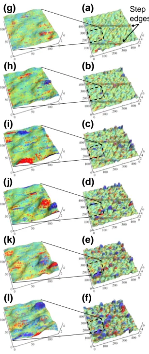
It is quite striking to observe that the topographic homogeneities (Fig.3a) that appear through the pulse in-duce MIT transition, absent in the pristine material, are perfectly correlated to the induced metallic and super-insulating patches, as demonstrated on the 3D topog-raphy/spectroscopy map of Fig.3f. In this image the 3D channel corresponds to the topography and the color channel corresponds to the conductance map at -200 mV. It is clear from this picture that the material inflates where new electronic patches appear, indicating that a very strong electron-lattice coupling is involved in the MIT. This strong electron-lattice coupling is reminiscent
4
(f)
(e)
(d)
(c)
(l)
(k)
(j)
(i)
(h)
(a)
(b)
(g)
Step edgesFIG. 4: (Color online) The right part from a to f displays a se-ries of consecutive Topographic/Spectroscopic measurements conducted on the same area (scale in nm). The topography was acquired with at VT = −630 mV, IT = 250 pA. The 3d canal correspond to topography while the color canal corre-spond to the conductance map at -200 mV. The left part of the figure, from g to l, show zooms on a same area, where switchings between insulating, metallic and super-insulating state are observed during consecutive frames. The topogra-phy is clearly correlated to the local electronic transitions.
of the volume change encountered in the Mott metal-insulator transition such as in the canonical Mott insu-lator V2O3[25].
We have therefore strong indications that the electric field applied with macroscopic external electrodes (Fig.1) creates an electronic phase separation concomitant to strong local sample deformations. At this step we may also expect that the strong electric field generated by the STM tip could locally modify the electronic state. Fig-ure 4 shows successive topographic/spectroscopic maps measured on the same location of a transited crystal. The successive topography and conductance maps reveal that between two consecutive measurements, some zones switch back and forth between the super-insulating, in-sulating and metallic states (see the zooms on figure 4). Such switchings however, while being certainly due to an interaction between the STM tip and the sample, are not observed during purely topographic measurements, even after consecutive scans over 24 hours, if the bias volt-age was kept lower than ∼ 700 mV. The fact that the switchings are observed only during spectroscopy mea-surements indicates that the electronic phase separation
in GaTa4Se8 is strongly affected by the voltage sweeps
(±1V) applied trough the STM tip. This supports the existence of a threshold field, in agreement with the con-clusions of macroscopic experiments [18, 19]. Finally we note that the use of high voltage pulses (∼ 2 V) well above the threshold voltage to selectively induce new electronic phase appears to be impossible since the lo-cal inflation of the material during the pulse is so strong that the surface ‘jumps’ to the tip at every pulse and provokes tip crashes [26].
In conclusion, the comparison of our STM/STS data acquired on pristine and transited crystals gives a di-rect experimental evidence that the electric-field-induced
metal-insulator transition recently observed in GaTa4Se8
arises from the formation of a nanoscale electronic phase separation. The pristine crystals are homogeneous while the transited crystals display a peculiar electronic patch-work with a filamentary structure, that consists of a metallic/super-insulating network embedded in a barely pristine insulating matrix. The induced electronic inho-mogeneities are associated with local topographic infla-tions indicating an important strain effect in the induced phase separation, probably originating from a strong electron-lattice coupling. The electronic phase separa-tion can be reorganized by the electric field of the STM tip, suggesting that a local electric field might be used in this correlated systems to tune the Mott metal-insulator transition at the nanometer scale at room temperature.
The authors thank J. Martial at IMN for her skilled help in sample preparation. This work was supported by Grants ANR-05-JCJC-0123-01 (to L.C., B.C. and E.J.) and ANR-09-Blan-0154-01 from the French Agence Na-tionale de la Recherche.
[1] M. Fath, S. Freisem, A. A. Menovsky, Y. Tomioka, J. Aarts, J. A. Mydosh, Science 285, 1540 (1999)
[2] Ch. Renner, G. Aeppli, B.-G Kim, Yeong-Ah Soh, S.-W Cheong, Nature 416,1540 (2002)
[3] T. Becker, C. Streng, Y. Luo, V. Moshnyaga, B. Dam-aschke, N. Shannon, K. Samwer, Phys. Rev. Lett. 89,237203 (2002)
[4] T. Cren, D. Roditchev, W. Sacks, J. Klein, J.B. Moussy, C. Deville-Cavellin, M. Lagues, Phys. Rev. Lett. 84, 147 (2000)
[5] T. Cren, D. Roditchev, W. Sacks, J. Klein, Europhys. Lett. 54, 84 (2001)
[6] C. Howald, P. Fournier, A. Kapitulnik, Phys. Rev. B 64, 100504 (2001)
[7] S. H. Pan et al., Nature 413, 282 (2001)
[8] Ø. Fischer, M. Kugler, I. Maggio-Aprile, C. Berthod, C. Renner, Rev. Mod. Phys. 79, 353 (2007).
[9] M. Qazilbash, M. Brehm, B. G. Chae et al., Science 318 1750 (2007)
[10] A. Frenzel, M. M. Qazilbash, M. Brehm et al., Phys. Rev. B 80, 115115 (2009)
[11] Y. J. Chang, J. S. Yang, Y. S. Kim, D. H. Kim, T. W. Noh, D. W. Kim, E. Oh, B. Kahng, J. S. Chung, Phys. Rev. B 76 075118 (2007)
[12] C. Kim, Y. Oikawa, J. S. Shin, H. Ozaki, J. Phys. Con-dens. Matter 18, 9863 (2006)
[13] J. Zhang, R. G. Moore, S.-C. Wang,H. Ding, R. Jin, D. Mandrus, E. W. Plummer, Phys. Rev. Lett. 96, 066401 (2006)
[14] K. Iwaya, Y. Kohsaka, S. Satow, T. Hanaguri, S.
Miyasaka, H. Takagi, Phys. Rev. B 70, 161103(R) (2004) [15] J. G. Rodrigo, S. Vieira, P. Somasundaram, J. M. Honig, F. A. Chudnovsky, V. N. Andreev, Phys. Rev. B 58, 10256 (1998)
[16] M. Imada ,A. Fujimori, Y. Tokura, Rev. Mod. Phys. 70, 1039 (1998).
[17] C. Vaju, L. Cario, B. Corraze, E. Janod, V. Dubost, T. Cren, D. Roditchev, D. Braithwaite, Adv. Mat. 20,2760 (2008)
[18] L. Cario, C. Vaju, B. Corraze, V. Guiot, E. Janod, Adv. Mat. 22,5193 (2010)
[19] E. Souchier, L. Cario, B. Corraze, P. Moreau, P. Ma-zoyer, C. Estoun`es, R. Retoux, E. Janod, M.-P. Besland, Physica Status Solidi - Rapid Research Letters, 5, 53-55 (2011)
[20] M. M. Abd-Elmeguid, B. Ni, D. Khomskii, R. Pocha, D. Johrendt, X. Wang,K Syassen, Phys. Rev. Lett. 93,126403 (2004)
[21] H. Ben Yaich, J. C. Jegaden, M. Potel, M. Sergent, A. K. Rastogi, R. Tournier, J. Less-Common Met. 102,9 (1984) [22] R. Pocha, D Johrendt, B. F. Ni, M. M. Abd-Elmeguid,
J. Am. Chem. Soc. 127, 8732 (2005).
[23] C. Vaju, L. Cario, B. Corraze, E. Janod, V. Dubost, T. Cren, D. Roditchev, D. Braithwaite, Microlelec. Eng. 85, 2430 (2008)
[24] V. Ta Phuoc, private communication.
[25] D. B. McWhan and J. P. Remeika, Phys. Rev. B 2, 3734 (1970)
[26] V. Dubost, T. Cren, C. Vaju, L. Cario, B. Corraze, E. Janod, F. Debontridder, D. Roditchev, Adv. Funct. Mat. 19, 2800 (2009)