En vue de l’obtention du
DOCTORAT DE L’UNIVERSITE DE TOULOUSE
Délivré par :
Université Toulouse 3 Paul Sabatier (UT3 Paul Sabatier) Présentée et soutenue par Chunxiang CHEN
Le 19 Juillet 2016
Design, synthesis and characterization of new organic
semi-conductors for photovoltaics
Ecole doctorale et discipline ou spécialité :
ED SDM : Sciences et Génie des Matériaux
Unité de recherche :
CNRS-UPR 8241 Laboratoire de Chimie de Coordination
Directrice de thèse :
Dr. Kathleen MOINEAU CHANE-CHING
Jury :
Philippe LAINE Directeur de Recherche – ITODYS Rapporteur
Arnaud MARTEL Professeur – I.U.T Le Mans Rapporteur
Fabienne ALARY Professeure– LCPQ-IRSAMC Examinatrice
Zéphirin MOULOUNGUI Directeur de Recherche, INP-ENSIACET Examinateur Kathleen MOINEAU
First of all, I would like to express my deepest gratitude to my thesis advisor Dr. Kathleen I. Moineau-Chane Ching for providing me all the opportunity to do this research, her enthusiastic and patient guidance, continuous and unconditional support, and good advice throughout the project greatly encouraged and helped me, which has profound impact on me. I was sincerely honored to meet and work with her, because she is so knowledgeable, hard-working, rigorous and prudent attitude towards science, kind and warm-hearted, and so on. I highly appreciate and never forget the time spent with her.
I would like to extend warm thanks to the whole team "Molecules and Composites for Optics" which is directed by Prof. Isabelle Malfant, for their attention and expert advice for my work which contribute to the success of this thesis. Their knowledge, guidance, skills and confidence were the driving forces for my work. It’s my great pleasure to work with them throughout these 3 years. Thanks to the team, my stay in LCC was an unforgettable memory in many aspects of my life. I’m also grateful to all group mates and collaborators in LCC who have helped and inspired me in many aspects during the period of my study in France, in particular Dr. Daniel Hernandez Maldonado, Damien Le Borgne with whom I had many helpful and encouraging discussions.
I’m also much thankful to Dr. Fabienne Alary and Dr. Jean-Louis Heully from
Laboratoire de Chimie et Physique Quantiques (LCPQ) in Toulouse, for their involvement in the project. I learned a lot about theoretical calculation from them, their enthusiasm, help and guidance are highly appreciated.
Apparently, it’s impossible to achieve all the goals without the help of all the technical and administrative services of Laboratoire de Chimie de Coordination, because they are fundamental parts of daily work in LCC. Thanks to them for providing good work conditions and environment.
I give special thanks to my committee members: Dr. Philippe Lainé (ITODYS), Prof. Arnaud Martel (IMMM), Dr. Zéphirin Mouloungui (INRA) and Dr. Fabienne Alary (LCPQ) for their time, helpful comments and interest in my work.
and help of Dr. Wei Shen and Dr. Rongxing He, who are my previous Master supervisors from the Southwest University in China.
Many thanks to all my friends (here and elsewhere), the friendship were previous wealth of my life, which made my stay in Toulouse (and in China) an unforgettable memory.
I would like to acknowledge the financial support from the China Scholar Council (CSC) for offering me the abroad study opportunity and supporting my research in France.
For the last but not least, my sincere gratitude goes to my families in China and in France, for their love and never-ending support. Thanks to them, my life in France is wonderful and impressive. Like a motto in French: la vie est belle. Specifically, many thanks to my husband Dr. Yohan Dall’Agnese not only for his endless and deep love, but also for his thoughtfulness, generous help, support and encouragement in all aspects of my life, especially during the hard time of my thesis writing.
AM Air Mass means the proportion of atmosphere that the sunlight must travel through before radiating at the Earth’s surface (or sea level) relative to its overhead path length, and AM=1/cos(θ) (zenith angle, namely where θ is the angle from the vertical)
AM0 the standard spectrum outside the Earth's atmosphere that is typically used for power applications of solar cells in space
AM1 refers to the spectrum after passing through the atmosphere (perfectly clear and cloudless sky) at the Earth’s surface when the sun is directly overhead (θ=0°)
AM1.5 corresponds to a solar zenith angle of θ=48.2°, 1.5 atmosphere thickness that is useful to represent the overall yearly average for temperate latitudes
AM1.5G stands for the standard spectrum at the Earth's surface where the G represents global and involves both direct and diffuse radiation
AM2 corresponds to a solar zenith angle of θ=60° which is useful to predict wintertime performance of cells in temperate latitudes
HOMO highest occupied molecular orbital
LUMO lowest unoccupied molecular orbital
SOMO a singly occupied molecular orbital
Eg energy gap, refers to the difference (in electron volts) of energy between the bottom of the conduction band and the top of the valence band of the electrons in solids, related to energy difference between the HOMO and LUMO in chemistry
Isc the short-circuit current, corresponds to the maximum current from a solar cell and happens when the voltage across the device is zero
Jsc theshort-circuit current density (mA/cm2)
Voc the open circuit voltage, represents the maximum voltage obtainable from a
solar cell that occurs at zero current
FF Fill factor, a parameter which, in relevance with Voc and Jsc, evaluates the maximum power from a solar cell. The FF is equal to the ratio of the highest power from a solar cell to the product of Voc and Jsc
performance of a solar cell and compare the performance of one solar cell to another
OFET Organic Filed Effect Transistors
OLED Organic Light Emitting Diodes
OPVs Organic Photovoltaics
ITO Indium tin oxide
NBS N-bromosuccinimide
THF Tetrahydrofuran
DCM Dichloromethane
DCB Dichlorobenzene
DMA N,N-Dimethylacetamide
P3HT Poly(3-hexyl thiophene) (C10H14S)n, N° CAS : 108568-44-1
PC61BM or PCBM, or PC60BM, [6,6]-phenyl-C61-butyric acid methyl ester N° CAS : 160848-22-6
PC71BM or PC70BM, [6,6]-phenyl-C71-butyric acid methyl ester N° CAS : 609771-63-3
(C17H24O2)n, N° CAS : 138184-36-8
MDMO-PPV Poly [2-methoxy-5-(3,7-dimethyloctyloxy)]-1,4-phenylenevinylene
PCPDTBT Poly[2,1,3-benzothiadiazole-4,7-diyl[4,4-bis(2-ethylhexyl)-4H-cyclopenta[2,1-b:3,4-b']dithiophene-2,6-diyl]] (C31H38N2S3)n, N°CAS: 920515-34-0 PSBTBT Poly[(4,4’-bis(2-ethylhexyl)dithieno[3,2-b:2’,3’-d]silole)-2,6-diyl-alt-(2,1,3-benzothiadiazole)-4,7-diyl] PCDTBT Poly[[9-(1-octylnonyl)-9H-carbazole-2,7-diyl]-2,5-thiophenediyl-2,1,3-benzothiadiazole-4,7-diyl-2,5-thiophenediyl] (C43H47N3S3)n, N°CAS: 958261-50-2 PTB7
General introduction ... 1
Chapter I : Bibliography ... 5
I Renewable solar energy ... 5
II Organic photovoltaics ... 6
II. 2 Functional principle of organic photovoltaic cells ... 9
II. 2-1 Photon absorption and excitons generation ... 11
II. 2-2 Diffusion and dissociation of excitons ... 12
II. 2-3 Transport of charge carriers and charge collection ... 13
II. 3 Characterization of OPV performance ... 14
II. 3-1 Test conditions for OPV - standard solar spectra ... 14
II. 3-2 Important parameters for OPV efficiency ... 15
II. 3-3 Power conversion efficiency (PCE) ... 19
II. 4 Types of OPV and their architectures ... 20
II. 4-1 Bilayer heterojunction ... 20
II. 4-2 Bulk heterojunction ... 21
II. 4-3 Tandem OPV cells ... 23
II. 5 Organic semiconducting materials for OPVs... 24
II. 5-1 Introduction of semi-conductor property and π-conjugation ... 24
II. 5-2 Optical properties of semiconducting polymers ... 26
II. 6 Outlook ... 38
III PhD objectives ... 40
Chapter II : Molecular design ... 45
I Introduction ... 45
I. 1 Theoretical work on molecular design ... 45
I. 2 Theoretical work on active-layer interface ... 47
II Small molecules design ... 48
II. 1 Small molecules based on benzothiadiazole (Bz) core ... 49
II. 2 Small molecules based on dithienosilole (DTS) core ... 51
II. 3 Small molecules based on subphthalocyanines (SubPcs) ... 56
III Theoretical calculation ... 60
III. 1 Bz-based small molecules ... 60
III. 1-1 Electronic and optical properties ... 60
III. 1-2 Effect of fluorine substitution ... 67
III. 2 DTS-based small molecules ... 70
III. 3 SubPcs-based small molecules ... 72
IV Conclusion ... 75
Chapter III : Green chemistry approach for materials synthesis ... 79
I Introduction ... 79
Bz(T1CHO)2, Bz(T2CHO)2 and target molecules ... 82
II. 1-1 Synthesis of compounds Bz(T1CHO)2 and Bz(T2CHO)2 ... 82
II. 1-2 Environmental and economic aspects ... 85
III Synthesis of molecules based on dithienosilole (DTS) core ... 89
III. 1 Synthesis of mono-substituted compounds and related BzT2CAO molecule .... 89
III. 1-1 Synthesis of fragment BrBzT1CHO ... 89
III. 1-2 Synthesis of fragment BrBzT2CHO ... 93
III. 1-3 Synthesis of another Bz-based unsymmetrical molecule (BzT2CAO) ... 93
III. 2 Synthesis of DTS cores and DTS-based target molecules ... 94
IV Subphthalocyanine (SubPc) derivatives: synthesis and axial substitution ... 97
IV. 1 Synthesis of chloroboron subphthalocyanine (SubPcBCl) ... 97
IV. 2 Axial substitution of SubPcBCl ... 98
V Conclusion ... 99
Chapter IV : Materials characterization ... 103
I Optical properties ... 103
II Electrochemical properties ... 109
III Thermal properties ... 114
IV Structural properties ... 115
V Conclusion ... 118
II Computational details ... 122
III Films elaboration ... 123
IV Synthetic procedure ... 123 General conclusion ... 143 Future work ... 144 Annexes ... 149 Figure list ... 171 Scheme list ... 179 Table list ... 183 Résumé de thèse ... 187 References ... 209
1
General introduction
Energy is nowadays the most important and urgent problem facing humans, and the global demand for renewable energy is growing ever faster. Fossil fuels such as oil, gas, coal and other non-renewable energy are the main energy sources human consumed in the last century, their production and combustion have become a serious issue of our ecological environment, because of the large amount of carbon dioxide (CO2) emission, a key driver of global warming. The fossil fuels are not able to meet the future need due to their limited resources and sky-rocketing price, leading to ever urgent need for clean, renewable and sustainable energy sources. To achieve this goal is one of humanity’s greatest challenges. The sun can provide our planet an inexhaustible and endless source of energy, and the Earth receives sufficient solar energy per hour to satisfy humans’ annual demand. The energy irradiated on the Earth’s surface from the sun each year is twice as the energy of all fossil and nuclear energy stores. Solar energy is therefore a promising alternative to these non-renewable energy sources and will play a significant role in meeting increasing energy demands.
The organic photovoltaic cells (OPV cells) promise to provide solar-to-electric energy conversion. It is one of the most important and promising long-term strategies for providing clean and renewable energy to our planet. It have attracted widespread attention as promising candidates to meet the increasing demand for renewable energy, due to their outstanding properties, such as ease of fabrication, mechanical flexibility, potential for renewable and green energy source low-cost potential, etc.(1-5) Currently, a record power conversion efficiency (PCE) of 13.2% for an OPV multi-junction cell was reached by Heliatek.(6) The development and synthesis of new organic semiconductors, that can be electron donor or acceptor for their use in the active layer is of great importance, together with technical progress in the device fabrication to reach OPV cells with high performance. Small molecules for OPVs have emerged as attractive candidates over their polymer counterparts, because of the well-defined but versatile chemical structures which allow easier energy level control, together with higher purity.
The work reported herein is focused on the development and synthesis of small molecules. The motivation is to obtain new small molecules for use as active materials via green synthesis within as simple as possible procedures. In this work, we investigated few new materials from initial design to synthesis and to characterization.
2
The first chapter is a bibliographic review. We explain the functional principle, important characterizations, and different types of organic photovoltaic devices before focusing on the state-of-the-art electronic materials for OPV devices. A summary of the performance of various organic π-conjugated materials used as donors or acceptors for OPV cells is given. The outlook on organic photovoltaics is summarized as the closing remark.
The second chapter focuses on theoretical calculations used for molecular design. In particular, a series of small molecules based on benzothiadiazole (Bz) core, 4,4’-di-n-octyl-dithieno[3,2-b:2’,3’-d] silole (or dithienosilole, DTS) core, and subphthalocyanines (SubPcs) unit are theoretically investigated. Their electronic properties are predicted via theoretical calculations using density functional theory (DFT). The synthetic strategies for obtaining these molecules are also described.
The third chapter describes the experimental synthetic methods used for the molecules previously designed. In particular, direct arylation methods used as a green synthetic approach are presented, as well as traditional Suzuki cross-coupling. The E-Factor (kg waste / kg product) for assessing the environmental impact of the two manufacturing processes is also given.
In the fourth chapter, four obtained Bz-based small molecules are investigated in terms of optical, electrochemical, thermal properties and structural properties. We identify these molecules as promising materials for applications in OPV cells.
The fifth chapter presents the experimental procedures related to the synthesized molecules throughout this work.
5
Chapter I : Bibliography
I Renewable solar energy
Currently, more than 80% (as shown in the following two figures) of the worldwide energy supply is from carbon-based fossil fuels like oil, coal, gas, and other non-renewable sources.(7) Their production and combustion have become nowadays a major problem of our environment due to the emission of huge amount of carbon dioxide (CO2), a dominant greenhouse gas and a key driver of global climate change. Use of fossil fuels has led to serious ecological problems (global warming, pollution, planet degradation) and economic concerns (limited resources while sky-rocketing price). Therefore, renewable energies are one of the hot topics of the global energy strategy. The demand to explore and develop renewable energy sources has become increasingly urgent.
Figure I-1: World total primary energy supply in 2013, provided by International Energy Agency. Coal: peat and oil shale are aggregated with coal, other: geothermal, solar, wind, heat, etc., are included.(7)
Among the renewable energy resources: biomass, hydropower, geothermal, wind and solar, the inexhaustible solar energy appears as one of the most promising energies.(8) The sun represents the most powerful energy source available on earth. The energy received from sunlight striking the earth surface in 1 hour (120 000 TW, consisting of 5% ultraviolet, 43% visible and 52% infrared, as plotted in Figure I-3) is far more than all of the energy consumed on our planet in an entire year.(9, 10) Consequently, the use of solar energy is one of the most significant challenges nowadays in scientific community.
6
Figure I-2: U.S. energy consumption by energy source in 2014. Source: U.S. Energy Information Administration.(11)
Figure I-3: The spectrum of solar radiation.(12)
II Organic photovoltaics II. 1 Introduction
Organic photovoltaic cells (OPVs) which convert directly solar energy into electrical energy are considered as one of the most promising long-term and cost-effective solutions to meet the demand of clean and renewable energy source for our planet. OPVs therefore have attracted great concern in both science and industry.(3, 13-31) The common building block of an organic photovoltaic system consists of one or several photoactive organic materials sandwiched between an anode and a cathode. A randomized network of active materials
7
blending is often used as the organic photovoltaic system. It is named as a bulk heterojunction (BHJ). Figure I-4 depicts a BHJ-based organic photovoltaic device (OPV). The often used anode is indium tin oxide (ITO) coated on a glass substrate modified with an interfacial layer based on poly(ethylenedioxythiophene):poly(styrene sulfonic acid)(PEDOT:PSS) which offers good charge transport. The cathode is typically a low work function metal. The most frequently used cathode according to the literature is aluminum. Poly-(3-hexylthiophene) (P3HT) and [6,6]-phenyl-C61-butyric acid methyl ester (PCBM) blend is one of the most commonly used photoactive layer.(32) P3HT and PCBM are the most common electron donor and electron acceptor, respectively. The detailed photovoltaic process in organic photovoltaic cells will be given below (section II.2). There are mainly two kinds of organic materials for photovoltaic cells: polymers and small molecules. A common feature of both polymers and small molecules is that both of them are constituted of large -conjugated systems.
Figure I-4: Device architecture of a bulk heterojunction photovoltaic cell.
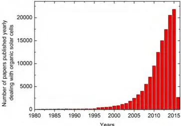
OPV cells have drawn more and more attention from both academic and industrial researchers, as evidenced by the evaluation of the numbers of articles concerning organic solar cells and published in international journals over the last three decades (see Figure I-5).
Figure I-5: Number of publications dealing with organic solar cells during the period of 1980-2016 (Source Scopus).
8
As shown in Figure I-5, a big rise occurred in the very beginning of the last ten years, and the interest in organic solar cells is steadily continuing and increasing. Figure I-6 shows the best research-cell efficiencies for a variety of photovoltaic technologies, with leading efficiencies for inorganic multijunction cells up to 46%, and with efficiencies of single crystalline and multicrystalline Si cells surpassing 27% and 25%, respectively. Although these high efficiencies are appealing and promising, they are not the only standard for evaluating the potential of these technologies. The overwhelming drawbacks of these inorganic photovoltaic technologies are their high production costs owing to the amount of materials needed for these devices and vacuum processing demanded for production, as well their high fabrication costs.(32) Besides, inorganic silicon solar cells are expensive, rigid, heavy, and complicated to produce. Organic photovoltaic cells based on π-conjugated small molecules and polymers
Figure I-6: The latest chart on record cell efficiencies, provided by The National Center for Photovoltaics (NCPV) at National Renewable Energy Laboratory (NREL).(33) Progress in photovoltaic power conversion efficiencies is tracked six monthly by Green
et al.(34)
are part of an emerging photovoltaic technology with best power conversion efficiencies (PCEs) for both triple-junction (25) and single-junction achieving 11.5% (21), with appealing properties such as low cost, light weight, flexibility, transparency, solution processability, printability, portability and large-area fabrication compatibility.(4, 14, 19, 20, 24, 26-28,
35-50) The photovoltaic effect, namely, the transform of light into electricity, can be tracked to
the pioneering studies of Becquerel in liquid electrolytes in 1839 (51) and has been investigated for a wide range of materials. It took quite a long time before the first report by
9
Chapin et al. in 1954 (52) on a silicon-based single p-n junction device with an efficiency of 6%. Almost 30 years after, Tang et al.(1) developed a two-layer organic photovoltaic cell and reported the first thin-film OPV cell affording a power conversion efficiency of about 1% in 1986. Hereafter, organic photovoltaics have become one of the state-of-the-art issues in science, as illustrated by the blooming and fruitful publication numbers shown in Figure I-5. The OPV performances have been improved steadily to power conversion efficiencies over 11% (see Figure I-6).(21, 25) In addition, the considerable contribution from world-wide industries such as Solarmer (USA), Heliatek (Germany) and so on, has so far leaded OPV to a new record power conversion efficiency of 13.2% set by Heliatek R&D teams (6) on 8 February, 2016.
Organic photovoltaic cells belong to a significant emerging technology in the modern era. It could facilitate the ever broader use of solar energy in coming years, wherever clean, renewable energy is needed, not only for industries such as building and construction materials, but also automotive, light architectural structures and flexible devices.
II. 2 Functional principle of organic photovoltaic cells
Contemporary organic photovoltaic cells are often based on a heterojunction made of two materials: an electron donor (D) and an electron acceptor (A). In the molecular case, the basic energy level diagram used to describe the operating principle of an OPV cell is shown in Figure I-7. The molecular energy levels involved in the light conversion into electricity are the highest occupied molecular orbital (HOMO) and the lowest unoccupied molecular orbital (LUMO), respectively. The ionization potential (IP) is the energy needed to remove an electron from a neutral molecule, and is related to the HOMO energy level. The fundamental gap, Efund or HOMO-LUMO energy gap is defined as the difference between IP and the electron affinity (EA).(53) The EA is the amount of energy released when an electron is added to a neutral molecule. EA is used to estimate the electron-withdrawing ability of a molecule to act as an electron-acceptor in an OPV device, and is thus linked to the LUMO energy level relative to vacuum.
10
Figure I-7: Basic energy level diagram and illustration of energy gap in molecular case of an organic semiconductor.(53)
S0 indicates the (singlet) electronic ground state and S1 denotes the lowest (singlet) excited state (here considered to be available via one-photon absorption). The energy difference between S1 and S0 is called the optical gap (Eopt (eV)), given by the equation:(54)
E= hc / λ (1)
Where h is Planck's constant (6.626 × 10 -34 J·s) and c is the speed of light (2.998 × 10⁸ m·s-1), and hc = 1240 eV· nm, thus
E (eV) = 1240 / λ (nm) (2)
Eopt is generally lower than the Efund, which is ascribed to the electrostatic bound between electron and hole in the excited state contrary to the ionized state. The exciton (or electron-hole pair) binding energy EB is the difference between fundamental gap and the optical gap, given by Figure I-7:
EB = Efund - Eopt (3)
In the material case, the molecular energy levels are broadened into electronic bands. The upper occupied band is referred to as the valence band and the lower unoccupied band is referred to as the conduction band. The material band gap is defined as the energy difference between the top of the valence band and the bottom of the conduction band.
As simply described in Figure I-8, the photovoltaic effect of converting sunlight into electricity in an organic photovoltaic cell can be summarized as the following four steps:(27,
55) (i) Photon absorption and excitons generation; (ii) excitons diffusion to the D/A interface;
(iii) excitons dissociation into free charge carriers (electrons and holes), and (iv) charge transport and charge collection at the electrodes, which produces current in the external circuit.
11
Figure I-8: Functional principle of a D/A solar cell.
II. 2-1 Photon absorption and excitons generation
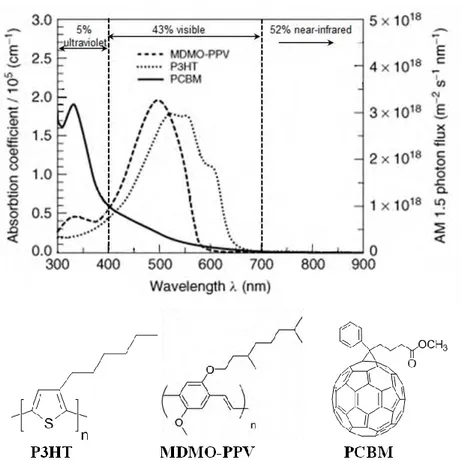
For efficient photon absorption, the absorption spectrum of the photoactive layer should match the solar spectrum and the layer should be adequately thick to absorb the maximum of the incident solar light. Due to the relatively large band gap in organic materials, only a small portion of the sunlight is absorbed (see Figure I-9(up)). For example, the conjugated polymers MDMO-PPV and P3HT (two of the most commonly used donor polymers) show poor absorption in the red and NIR part of the solar spectrum, and PCBM (the most widely used acceptor polymer) shows a low extinction coefficient at visible and near-IR wavelengths, thus, the polymer donor is the dominant light-absorbing component in a photovoltaic blend. The chemical structures of these commonly used materials are provided in Figure I-9(down). The band gap, evaluated from the onset of the absorption band, are of 580 nm and 660 nm (i.e. 2.13 eV and 1.88 eV) for MDMO-PPV and P3HT, respectively.(37) A material presenting a band gap of 1.1 eV (1100 nm, Eopt (eV) = 1240/ λ (nm) ) is able to absorb 77% of the solar emission on the Earth surface, while the band gap of most of the semiconducting polymers is larger than 2 eV (620 nm) which restricts the possible harvest of solar photons to around 30%.(14, 37, 55) Thus, it is possible to harvest more sunlight and as a result, an increase in the photocurrent can be prospected by lowering the band gap of organic semiconductors. In addition, since the absorption coefficients of organic materials are as high as 105 cm-1 (see Figure I-9(up)), a thickness of active layer of only 100 nm is sufficient to absorb most of the incident photons.(55) Increasing the layer thickness might hamper charge transport and therefore lower the fill factor (see II-3.2), though it is often favorable to light absorption.
12
Figure I-9: Absorption coefficients of films of commonly used materials are depicted in comparison with the standard AM 1.5 terrestrial solar spectrum (up)(according to Ref.(56)), and the structures of the materials (down).
Unlike what happens in inorganic semiconductors, and owing to the low dielectric constant of organic materials, the photon absorption at room temperature in organic materials results in coulombically bound neutral electron-hole pairs (excitons), rather than free charge carriers. The exciton binding energy is in the range of 0.35 - 0.5 eV.(57) That is the reason why an electron donor/electron acceptor interface is needed in OPV devices to provide a driving force for the dissociations of excitons and the generation of free charge carriers.
II. 2-2 Diffusion and dissociation of excitons
For achievement of high power conversion in OPV, the maximum of excitons generated due to light absorption should give rise to the formation of free charge carriers (electron and hole). It is shown that only 10% of the incident photons result in free charge carriers generation in conjugated polymers.(58) One of the reasons for this low percentage is the low exciton lifetime (10 to 400 ps).(59) As a consequence, the order of magnitude of exciton diffusion length should be the same as the size of the photoactive domain, which limits the component thickness.(60) Otherwise, excitons decay via luminescence or non-radiative recombination to
13
the ground state, which is in competition with exciton diffusion before reaching the interface. Generally, exciton diffusion lengths in organic semiconductors are of about 10-20 nm.(55)
Charge dissociation is one of the subsequent key steps for sunlight conversion into electricity. In this step, the exciton is split in free charge carriers, the electron is transferred to the electron acceptor material and the hole to the electron donor material. Blending conjugated electron-donor polymers with electron-withdrawing materials such as the commonly used fullerene derivatives is a quite effective method for forming a charge transfer state (CTS). The CTS can be regarded as a state in which charge carriers are coulombically bound across the D/A interface. It is possible to promote charge dissociation from CTS when the energy offset (ΔE) between the LUMO of donor and the LUMO of acceptor is larger than the exciton binding energy. The minimum offset required for charge separation is approximately 0.3 eV.(61-63) Then the photoinduced charges can migrate to their corresponding electrodes. Therefore, the effect of charge recombination processes should be reduced or avoided as much as possible.
II. 2-3 Transport of charge carriers and charge collection
For efficient photovoltaic cells, the separated charges are required to be transported to the suitable electrodes within their lifetime which is estimated to be the order of magnitude of a few µs at 295 K.(64) The dominant driving force is the internal electric field created by the equalization of the Fermi energy levels of the two electrodes. Under the influence of the electric field, the charges remain separated (and thus no recombination after exciton dissociation) and migrate to the organic layers.(62) Thus, the work functions of the electrodes (or of the charge transport layers) are determinant and require a careful choice of the electrode metals (and the interface layers). In addition, transport of charge carriers is strongly affected by charge recombination during the charge transport to the electrodes, especially if the transport medium for both holes and electrons is the same material.(60) Therefore, charge carries recombination process should adequately slow down to let charge carriers reach the electrodes. Thus, the charge carrier mobilities (strongly dependent on the molecular organization of the material) through the active layer are determinant and require careful control on the active layer morphology. An important objective for OPV cells is to minimize the energy and charge loss processes for the purpose of improving the device efficiencies. As the last step, charge carriers are collected from the device via two selective contacts (see Figure I-4). Usually, an indium tin oxide (ITO) due to its large optical transparency and high
14
conductivity serves as the anode on one side, matching the HOMO levels of donor.(65) A low work function metal serves as the cathode on the other side of the device. The most often used cathode is evaporated aluminum which possesses a work function of around 4.3 eV,(66) matching the LUMO of acceptor PCBM.
II. 3 Characterization of OPV performance
II. 3-1 Test conditions for OPV - standard solar spectra
Various solar spectra conditions based on different spectral distributions are used for photovoltaic characterization, thus it is important to have a standard reference spectra in order to allow the reproducibility of characterization and comparison of photovoltaic devices from different research laboratories and manufacturers. The standard spectrum outside the Earth's atmosphere that is typically used for power applications of solar cells in space is AM0 (in red on Figure I-10), which has an overall power of 1366.1 W/m2.Herein Air Mass (AM) means the proportion of atmosphere that the sunlight must travel through before striking at the Earth’s surface (or sea level) relative to its overhead path length, as shown in Figure I-11, and
AM is equal to Y/X, namely, AM = 1/cos(θ) (where θ is the angle from the vertical, zenith
angle). AM1 refers to the spectrum after passing through the atmosphere (perfectly clear and cloudless sky) at the Earth’s surface when the sun is directly overhead (θ = 0°). AM2 corresponds to a solar zenith angle of θ = 60° which is useful to predict wintertime performance of cells in temperate latitudes.
Figure I-10: Standard Solar Spectra for space and terrestrial use. (Source: pveducation)
The standard solar spectrum at the Earth's surface is named AM1.5G (67)(the G represents global and includes both direct and diffuse radiation, in blue on Figure I-10) or AM1.5D (the D means direct and which involves direct radiation only, in green on Figure I-10), where Air mass 1.5 (AM1.5, 1.5 times thickness of Earth’s atmosphere normal to Earth’s surface)
15
corresponds to a solar zenith angle of θ = 48.2° (see Figure I-10). Photovoltaic cells are usually tested at a temperature of 298K (25°C) under AM1.5G condition, simulating the 48.2°C irradiation from the sunlight to the ground. Under this condition, the incident power per unit area of the incident light is 1000 W/m2 (100 mW/cm2).
Figure I-11: Scheme of the sunlight path length, in units of Air Mass and dependent on the angle from the vertical (zenith angle θ). (Source: pveducation)
II. 3-2 Important parameters for OPV efficiency
The performance of OPVs is principally characterized by the power conversion efficiency.(13) There are three important photovoltaic parameters for evaluating photovoltaic performance: the open-circuit voltage (Voc), the short-circuit (photo) current density (Jsc), and the fill factor (FF). A typical current density versus voltage curve for a typical bulk heterojunction OPV device (see architecture provided in Figure I-4) in the dark and under illumination is illustrated in Figure I-12. All photovoltaic cells are photo diodes, which are able to create current or voltage from incident light when processing in reverse bias (where the voltage at the cathode is lower than at the anode). In the dark, as the orange dashed line showed in the current density versus voltage (J-V) curve, there is nearly no current flow until forward bias larger than the open circuit voltage are injected. When under illumination, as evidenced by the shift (blue solid line) in J-V curve, power is generated by the device.
Figure I-12: Current density versus voltage schematic diagram of organic solar cells in the dark and under illumination.
16
(a) Short-circuit (photo) current density (Jsc)
The short-circuit current density, Jsc, corresponds to the maximum current delivered under lighting by a solar cell and is measured when no voltage is applied to the device. Jsc is mainly determined by factors associated with each of the four steps described above. A broad absorption spectrum is favorable to harvest as much as possible of the photons from the solar light and would increase the Jsc value. For a given absorption outline of a given material, the bottleneck of charge carriers is the charge mobility which is sensitive to the nanoscale morphology of the organic semiconducting-material thin film.(68-72)
(b) Open-circuit voltage (Voc)
The open circuit voltage, Voc, represents the maximum voltage obtainable from a solar cell, and is measured when the current equals to zero. Experimentally, the HOMO and LUMO energy levels can be evaluated from the oxidation potential of the donor and reduction potential of the acceptor via electrochemical characterization. In organic photovoltaic cells, it has been reported that the Voc value is not exactly determined by the energy difference between the HOMO of the donor material and the LUMO of the acceptor at the interface.(73,
74) Its value also depends on that of the binding energy of the excitons.
Figure I-13: Schematic energy level diagram between an ideal polymer and a PC61BM
acceptor.(63)
The Voc of a conjugated polymer-PCBM photovoltaic cell (see Figure I-13) can be estimated by the Scharber model given the empirical equation:(61)
Voc = 1/e (
|
EDHOMO – EALUMO|
) – 0.3 V (4)Where e is the elementary charge, and the value of 0.3 V is an empirical factor. 0.3 V is found to be the deviations between the theoretical biggest built-in potential (VBI) and the Voc.(61) It is necessary that the electron acceptor material has a conduction band edge that is lower than
17
that of the electron donor material.(56, 75-77) A minimum energy offset between the LUMO level of the polymer donor and the PCBM acceptor of approximately 0.3 eV has been demonstrated necessary to achieve efficient electron transfer from the LUMO of polymer donor to the LUMO of PCBM acceptor.(61, 62, 78)
According to equation (4), to offer a high Voc, HOMO energy level of the donor can be decreased or LUMO energy level of the acceptor can be increased. However, such changes could simultaneously result in wider band gap and narrower absorption width, which means lower efficiency of photon absorption from the solar spectrum. Meanwhile, the LUMOs offset shown in Figure I-13 in BHJ should be larger than 0.3 eV.
In the Scharber model, the only inputs required are the HOMO and LUMO energy levels. The generated PCE values in the Scharber model should be understood as the potential performance that may be reached, if the assumptions can be met. These assumptions combine various additional conditions that have to be met to achieve a high-performance candidate, especially requirements associated with complicated optimization and control of BHJ active-layer morphology, interface behavior, and the dynamics of exciton and charge carriers. The standard parameters that reflect the assumptions in the Scharber model include a uniform external quantum efficiency of 65%, a fill factor (FF) of 0.65, a required LUMO offset of 0.3 eV between donor and acceptor for efficient charge separation, and an empirical loss parameter of 0.3 eV. However, there is no certainty that the top candidates will truly perform as well as expected, because their performances may be affected by various factors, such as morphology control, interface layer and device fabrication. It is indicated that the theoretical efficiency limit in the standard Scharber model is 11.1%, which requires energy levels of LUMO and HOMO of the ideal donor have to be -3.9 eV and -5.4 eV (Eg = 1.5 eV) respectively as the optimal parameter combination.
18
Figure I-14: Efficiency of a D/A OPV cell vs the band gap energy of the donor, and the LUMO offset between the two materials.(79)
Figure I-14 provides the efficiency of a D/A OPV cell versus the band gap energy of the donor and the offset between the LUMO of the donor and the LUMO of the acceptor, with the assumption that Voc obeys equation (4).(61) It is of great interest that the efficiency of the device keeps consistent with the LUMO offset (ΔE), precisely, the lower the offset, the higher the efficiency. Figure I-14 suggests that the photovoltaic efficiency of a BHJ solar cell should be more sensitive to variations of the LUMO offset compared to changes of the band gap of the donor. As a result, we can conclude that the choice of the D/A couple is as significant as the band gap of the donor material.
(c) Fill factor (FF)
The Fill factor (FF) is a parameter that is associated with Voc and Jsc, and evaluates the maximum portion of electric power that can be extracted from a photovoltaic cell. The FF can be given by the ratio of the electric power between the blue and purple areas the J-V curve (see Figure I-12), and defined by equation:
FF = Pmax / (Jsc x Voc) = (Jmax x Vmax) / (Jsc x Voc) (5)
Where Jmax is the current density and the voltage at the maximum or ideal power point, and Vmax is the voltage at the maximum or ideal power point. The FF provides a sign of how possibly charges can be extracted from a cell and is usually described as the “squareness” of the J-V curve, and will have a value of unity in an ideal case that corresponds to output power of Pideal. Alan J. Heeger (27) suggested that the FF in BHJ solar cells is affected by the
19
competition between charge carriers sweep-out by the internal voltage (built in electric field) and the loss of charge carriers by recombination. It is also indicated that the series and shunt resistances are two essential factors that affect the fill factor of a solar cell.(32, 56, 80) Besides, morphology is also of high influence on FF.(81)
II. 3-3 Power conversion efficiency (PCE)
As mentioned previously, the performances of terrestrial solar cells are measured under AM1.5G conditions with incident power of 100 mW/cm2 and at a temperature of 25°C. Power conversion efficiency (PCE) suggests the percentage of incident optical power that converts into electricity, and is defined as the ratio of output energy from a PV device to input energy from the solar spectrum. It is the most important and commonly used metric to determine the performance of a solar cell and compare it to the others. As sketched in the J-V curve, the maximum power point (Pmax) is localized on the J-V curve where the product of the current density and voltage is the highest.(56) To determine the efficiency of a solar cell, the output power requires to be compared to the input power, as indicated below:
PCE = Pmax / Pin = (Jmax x Vmax) / Pin (6)
According to equation (6), the maximum power created in the external circuit is the product of the fill factor, open circuit voltage and short-circuit current density. Consequently, the power conversion efficiency can be described as:(4)
PCE= (FF x Jsc x Voc) / Pin (7)
Where Pin represents the total power density of the incident light source. Therefore, the power conversion efficiency is mainly dependent on the three parameters: the open circuit voltage (Voc), the fill factor (FF), and the short-circuit current density (Jsc).
Furthermore, it is worth mentioning that external quantum efficiency (EQE) is a means for estimating the portion of current that can be generated by a special wavelength of light. It is defined as the number of charge carriers divided by the total number of incident photons. It shows the potential that one absorbed photon will lead to the generation of one electron that can flow through an external field. EQE indicates the overall efficiency of the four principle steps in the photovoltaic process, as given by equation (8):
EQE(λ) = ηA (λ) x ηED (λ) x ηCT (λ) x ηCC (λ) (8)
Here, ηA is the photon absorption efficiency, the exciton diffusion efficiency ηED is the portion of photoinduced excitons that reaches the D/A interface prior to recombination. ηCT is the charge transfer efficiency, and the charge collection efficiency ηCC is the potential that a free
20
charge carrier originated from excitons dissociation at the D/A interface reaches its respective electrodes, and λ is the wavelength of interest.(32, 82) It shows the closer of the EQE value to
1, the more efficient of current generation at a certain wavelength, with limited recombination loss. Clearly, decreasing recombination loss will offer higher EQE values.
II. 4 Types of OPV and their architectures
D/A heterojunction devices can be divided into two principal types of architectures: bilayer (or planar) heterojunction (1) and bulk heterojunction (BHJ) that was first reported in 1995(29, 35, 83).
Figure I-15: The architecture structure of (a) bilayer heterojunction and (b) BHJ OPV devices.(84)
II. 4-1 Bilayer heterojunction
In a bilayer heterojunction device, donor and acceptor materials are stacked sequentially with a planar interface as displayed in Figure I-15a. The photoactive layer is sandwiched between a high work function anode matching the HOMO of donor and a relatively low work function metal cathode matching the LUMO of acceptor, for efficient collection of the corresponding charge carriers. Figure I-16 shows the schematic energy level diagram of an OPV, revealing the anode and cathode work functions. Generally, a transparent indium tin oxide (ITO) (presenting a work function of -4.7 eV) and aluminum (presenting a work function of -4.3 eV) are the most commonly used anode and cathode, respectively.(85) Generally, bilayer heterojunction devices are achieved by vacuum deposition due to the difficulty to find proper solvents for donor and acceptor layers without damaging the D/A interface.(84)
The first reported thin-film organic photovoltaic cells was a donor/acceptor (D/A) heterojunction cell, which gave a power conversion efficiency of approaching 1%.(1) This first report paved the way towards higher power conversion efficiencies reached thanks to the development of enhanced active materials. The performance of bilayer based organic
21
photovoltaics is hampered by the short exciton diffusion length (5-20 nm) in organic materials,(55, 86) because the optimal thickness of the photoactive layer in planar architecture
is related to the exciton diffusion length. Therefore the optimal percentage of the incident light that the device can absorb and transform into electrical power is limited.
Figure I-16: Schematic energy level diagram of an OPV, revealing the anode and cathode work functions, the HOMO and LUMO offsets (ΔHOMO and ΔLUMO, respectively) and the maximum open-circuit voltage (Voc).(87)
The bilayer architecture is one of the most common types of OPV, but it causes efficiency loss not only due to excitons created too far away from the D/A interface, but also because of the low D/A interfacial area. One big advantage of bilayer heterojunction over single layer(56) is that holes and electrons can be effectively separated to reduce efficiency loss due to charge recombination after the excitons dissociation. But, it also constitutes a limit for high conversion efficiency, because the bilayer structures are primarily limited by the exciton diffusion length.(32)
II. 4-2 Bulk heterojunction
Due to the limitation of bilayer heterojunction, further evolution was achieved in polymer devices by means of blends of the electron-rich and electron-deficient materials (2, 35). Different from bilayer heterojunction device, the active layer is blend of bicontinuous and interpenetrating donor and acceptor materials in a bulk heterojunction (BHJ) device. The BHJ concept was created by Yu et al.(35) and Halls et al.(5) in 1995, which is one of the state-of-the-art device architectures for OPV so far. BHJ is resulted from phase separation in a 5-20 nm length scale of the donor and acceptor materials during spin-coating and solvent evaporation. It overcomes the exciton diffusion bottleneck (55, 86) by producing an intricate interpenetrating network (Figure I-15b), and also provides charge transport paths to facilitate the charge collection at electrodes for achieving photoelectric conversion. A typical BHJ solar cell,(28) as the architecture outlined in Figure I-15b. As for the bilayer case, the active layer is
22
sandwiched between anode and cathode. Holes and electrons are transported to anode and cathode respectively in a standard architecture. As indicated in the schematic energy level diagram of an OPV (see Figure I-16), the anode typically includes a high work function transparent conducting electrode that is coated with a conducting substrate, and adjusted with an interfacial layer favorable to hole selection and/or electron blocking. The most commonly selected materials used as anode are indium tin oxide (ITO) (presenting a work function of -4.7 eV) on glass substrates adjusted with a interfacial layer about 40nm thick based on poly(ethylenedioxythiophene):poly(styrene sulfonic acid)(PEDOT:PSS).(88) These materials are preferable because of their great optical transparency and good charge transport. A low work function metal with an electron selective layer is often selected as the cathode (as revealed in the schematic energy level diagram). The most commonly encountered cathode is aluminum not only due to its low work function value but also high reflectivity.
Bulk heterojunction can be fabricated via vacuum deposition or solution processing techniques. Soluble materials can be deposited from solution via spin coating. Some of small molecules can be deposited under vacuum via thermal evaporation, for instance, thin films of DCV5T-Me: C60 reported by Bäuerle et al.(89) was vacuum deposited in BHJ single layer. Active layers of metal phthalocyanine: C60 and DCV6T: C60 were vacuum processed in a tandem cell. Because vacuum deposition allows for good control of the layer thickness which is necessary for the optimization of the device stack with regard to optical interference effects.(90) Vacuum deposition for OPV devices in an efficient roll-to-roll-process developed by Heliatek is an innovative technology that meets pioneer spirit.(6) In addition, thermal annealing, as another method for the fabrication of bulk heterojunction device completed with a metal cathode, was used to improve the efficiency of polymer solar cells.(91) This effect was ascribed to polymer chain alignment, leading to an increase in the formation of an interfacial layer at the organic/cathode interface or the charge carrier mobility. Another effect of efficiency enhancement in BHJ cells was attributed to a confined geometry by using a metal contact during annealing, preventing the formation of a rough surface morphology while allowing for the formation of an interpenetrating donor–acceptor network.(82) Whereas solution-processed BHJ type architecture with a fullerene acceptor was first reported in 1995 by Yu et al.(35) and Halls et al.(5). Over the last decade, the solution-processed BHJ OPVs has shown dramatic improvement in power conversion efficiency from less than 1% in the earliest publications to 11.7% (21) in the very recent literature. The power conversion efficiency of OPV cells based on small molecules and polymers have improved steadily over
23
the past decade. Moreover, bulk-heterojunction OPVs based on small molecules (SM-BHJ) have become a competitive alternative to the more widely investigated counterparts based on conjugated polymers.(92) So far, the performance of both polymer-based BHJ (23, 25, 40,
93-100) and SM-BHJ (19, 85) are comparable, with power conversion efficiency over 10%.
BHJ is regarded as the state of the art active layer morphology so far, because the interfacial area between donor and acceptor phases in a bulk heterojunction is greatly improved. Therefore, compared to bilayer heterojunction, the bicontinuous, nanoscale and interpenetrating network formed in BHJ architecture leads to higher performance of the OPV devices.(56, 84, 101) The progress is mainly ascribed to the improvement of the D/A
heterojunction (1, 102) that acts as a dissociation position for the coulombically bound photon generated excitons. However, due to the complicated nanomorphology, a D/A blend is hard to control and optimize the active layer morphology.(68)
II. 4-3 Tandem OPV cells
A class of OPV technology is “tandem cell” architecture (as shown in Figure I-17(left)),(47) which is based on a multilayer structure that comprises two or even more independent active layers in series. It reveals numerous advantages for further improvement, as reviewed by Christoph J. Brabec et al. in 2009(79) and by Yang Yang et al. in 2013(103). It is sufficient to realize the practical application of plastic photovoltaics in rooftop solar panel.
Figure I-17: Schematic architecture of an organic tandem solar cell including two sub-cells with different and complementary absorption spectra.(79)
A wide band-gap material for the first cell and a relatively lower band-gap semiconductor for the second charge-separation layer with are typically used in the tandem cells.(32, 47, 104) The tandem architecture allows to address two particular weakness originated from the inherent properties of π-conjugated organic materials.(105-109) To begin with, the
24
combination of two semiconductors with different band gaps enables a wide absorption over a wide range of solar emission spectrum due to the complementary absorption spectra from each layer (see Figure I-17(right)). The power conversion efficiency of the tandem cell is inherently higher than that of a single cell made from the narrower band-gap material, resulting from the higher energy of electron-hole pair generated by photons compared to that of the energy gap that rapidly relax to the band edges respectively. Moreover, owing to the low mobility of the charge carriers, an addition in the thickness of the active layer enhances the internal resistance of the device, as a consequence, both the Voc and fill factor (FF) are improved.(110) Hence, the tandem cells are able to give a higher optical density over a broader fraction of the solar spectrum. In other words, the tandem cell structure is beneficial to the efficiency of light harvest. The organic tandem photovoltaic cells have showed the highest performance of a bulk heterojunction solar cell to date, achieving over 11%.(23, 25, 111) Specifically, a new record power conversion efficiency of 13.2% for a multi-junction
device had been set by Heliatek on February 8, 2016.(6)
However, one major issue with tandem cells is that the total current of the cell is limited by the current generated in the front or back cell which is lowest. Therefore, to make full use of a tandem cell, the current generated in each sub-cell should match each other. Determining by the specific absorption and charge carrier mobilities of semiconducting materials, tandem cells generally use thicker back cell than the front cell so that the photocurrent created in each sub-cell are balanced.(47, 112) Due to the number of sub-cells and required precision of various processing steps, the scale up to roll-to-roll production in tandem cells is even a greater challenge.
II. 5 Organic semiconducting materials for OPVs
Generally, organic semiconductors have a wide band gap above 1.4 eV but less than 3 eV, materials with a band gap above 3 eV are considered as insulators. Organic semiconductors have been the focus of considerable research due to their intrinsic properties.(13, 113) The explored applications of organic semiconductors include organic light emitting diodes (OLED)(114-116), organic field effect transistors (OFET)(117-119), and organic photovoltaics (OPV)(13, 14, 36, 40, 60).
II. 5-1 Introduction of semi-conductor property and π-conjugation
The molecular structure of organic semiconductors consistently contains a π-conjugated backbone, along which the carbon or hetero atoms (nitrogen, oxygen and sulfur) are sp2p
-25
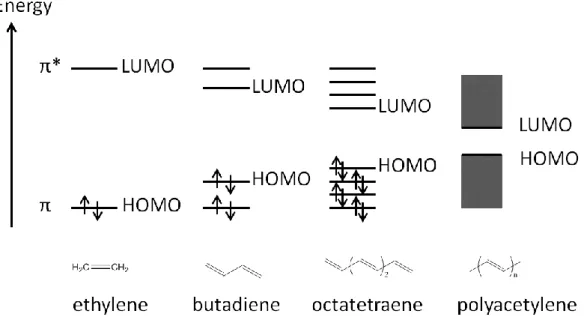
hybridized. The first classic example of a semiconducting polymer is polyacetylene (containing alternating single and double bonds, the structure and π orbital are showed in Figure I-18), which was studied in 1977 (120) by Hideko Shirakawa, Alan Heeger and Alan MacDiarmid who has been honored with the Nobel Prize in 2000 for their discovery and development of conductive polymers (121, 122). The π conjugation (overlap) along the
backbone leads to the formation of π orbital delocalization, relating to the molecular frontier orbitals (HOMO and LUMO) and determining the electronic and optical properties of the molecules or polymers.
Figure I-18: trans-polyacetylene and its schematic π orbital.
As sketched in Figure I-19, the frontier energy levels changes with the increase in the conjugation length in polyacetylene, which results in narrowing the band gap. The overlap of frontier π molecular orbitals between neighboring molecules or polymer main chains represents the strength of the intermolecular interactions (electronic coupling), which plays a key role in governing charge carrier mobilities. Different from crystalline inorganic semiconductors, which have a large charge carrier mobility owing to their three dimensional feature and rigid lattice, organic semiconductors generate more modest charge carrier mobilities because of formation of polarons (hole and electron) and localization of charge carrier. For organic semiconductors, the charge carrier mobilities strongly rely on the morphology, for instance, the charge carrier mobilities of highly disordered amorphous films (normally 10-6 to 10-3 cm2 V-1 S-1) can be enhanced over several orders of magnitude when making them highly ordered crystalline (over 1 cm2 V-1 S-1).(123)
26
Figure I-19: Illustration of energy binding mechanism with increase in the conjugation length of the ethylene in polyacetylene.
II. 5-2 Optical properties of semiconducting polymers
Normally, the sp2pz hybridized wave functions of the carbon atoms in repeat unit causes the π-conjugated electronic structure of polymers.(26, 121, 122, 124) As a schematic band diagram shown in Figure I-20(left), semiconducting polymers are depicted in aspects of the energy bands including the orthogonal π-bonds that generated by the pz wave functions and the bonding and anti-bonding σ-bands between neighboring carbon atoms. As provided in Figure I-20(right), the absorption of photons results in the migration of electrons from the valence band (π-band) to the conduction band (π*-band). As a result, mobile electrons and holes, which are responsible for the photoelectric conversion, are generated. The electrons and holes generated on a single chain relax fast to the respective band edges and, accordingly, either form neutral intrachain excitons or recombine when at energy hʋ>Eg. If the electrons and
holes are on isolated chains, polarons will be formed due to their self-localization.(121, 122,
124) The π-π* interchain stacking is a key parameter for the wave function of excitons spread
onto the adjacent chains (interchain transfer of excitons). The intrachain excitons can migrate, separate to produce polaron pairs on adjacent chains, go through intersystem crossing to the triplet state, or radiatively and non-radiatively decay to ground state.
27
Figure I-20: Schematic band diagram for π-conjugated polymers (left) and π-π* interband transition associated with generation of a mobile electron and a mobile hole in the π*-band and π-band respectively (right).(26)
II. 5-3 Charge transport mechanism in conjugated polymers
The morphology of polymeric materials plays a significant role in charge transport. It is worth noting that the mechanism of charge transport process in polymers is quite complex. Band transport and hopping are the main mechanisms of charge transport in conjugated polymers.(125) Band transport, often called intrachain transport, can be considered as exclusively for intrachain motion, which is the mechanism that should be conceived when considering conjugation. Hopping can be considered for both intrachain and interchain transport.(125) Here, hopping is a process by which charge carriers jump from one monomer or chain to another instead of transport coherently, which is considered to be very important in devoting to the charge carrier mobility. It is possible that a mix of band transport and hopping occurs in conjugated polymers (see Figure I-21b). It should also be noted that hopping can exhibit intrachain transport, as sketched in Figure I-21a. A defect or kink in a conjugated polymer will create the chance for charge to travel from one part of a chain to another without moving along the chain. Similarly, some non-conjugated materials show good semiconducting behavior with charge transport being exclusively owing to hopping.(125) Poly (vinyl carbazole) may be the simplest case of a polymer of which the charge transport mechanism is exclusively hopping (Figure I-21c).
28
Figure I-21: One difference of hopping transport from coherent (band) transport is that there is no need for charge carrier to move from one unit to the next. (a) This involves intrachain transport that may occur by a hopping mechanism, particularly when defects are existed in the chain. (b) It is possible that both coherent transport and hopping can occur in conjugated polymers, with the charge carrier hopping from one chain to another. (c) Only hopping transport exhibits in some polymers like poly(vinyl carbazole), due to lack of conjugated backbone.(125)
II. 5-4 Polymer-based and small molecule-based materials for OPV
Currently, organic photovoltaic donors are principally based on two types of electron-donating materials: polymers(14, 26, 29, 126-128) and small molecules (19, 20, 30, 45, 46, 84, 85, 92, 129-133), and OPV acceptors are mainly based on either fullerene or their
derivatives (3, 29, 35, 45, 127, 131) and fullerene-free materials including both polymer and small molecules) (22, 31, 128, 134-136).
(a) Polymer donors
Polymer-based BHJ solar cells have attracted great attention and been extensively investigated in science and industry because of their advantages such as solution processability, low cost, light weight, flexibility. Conjugated polymers are often built from blocks of electron-donating and electron-withdrawing units. As shown in Figure I-22, various central electron donor cores (thiophene, benzodithiophene (BDT), dithienosilole (DTS), dithienocyclopenta (DTC), dithienopyrole (DTP), silafluorene (SFL), fluorene (FL), carbazole (CZ), etc.), electron acceptor cores (2,1,3-benzothiadiazole (Bz), fluorinated benzothiadiazole (ffBz), triazole, thieno[3,4-b]thiphene, diketopyrrolopyrrole (DPP), thieno[3,4-c]pyrrole-4,6-dione (TPD), thieno[3,4-b] thiophene (TT) etc.), together with terminal units (dicyanovinyl, alkyl cyanoacetate, rhodanine, and 1,3-indanedione), as well as -conjugated bridges made of thiophene rings with different conjugation lengths have been used for the molecular design.(81, 137)
29
Figure I-22: Structures of some (a) electron donor and (b) electron acceptor units.
Polymer solar cells (PSCs) have been the leading candidates in OPV cells in the last decade. The chemical structures of some representative electron-donating materials based on donor and acceptor building blocks with high performance are illustrated in Figure I-23.
Figure I-23: Chemical structures of representative polymers acting as donors in OPV devices.
30
By far, methoxy-5-(2-ethylhexyloxy)-1,4-phenylenevinylene] (MEH-PPV), poly[2-methoxy-5-(3,7-dimethyloctyloxy)]-1,4-phenylenevinylene (MDMO-PPV), and poly(3-hexyl thiophene) (P3HT) have been the most studied π-conjugated polymers for use as donor components in BHJ devices. From the efficiencies in Table I-1, it is clear that PPV-based BHJ devices exhibit relatively poor performance, such as 2.3% and 2.5%. PCE as high as 3.3% was achieved in BHJ device based on MDMO-PPV which was blended with PC60BM as acceptor, attributed to active layer morphologies tune.(138, 139) Hereafter, P3HT-based BHJ devices have been thoroughly studied due to its lower band gap (1.9 eV) (as shown in Table I-1) which leads to a remarkably higher current density of more than 10 mA/cm2, as well as its enhanced π-stacking and crystallinity which results in a higher hole mobility.(140-142) An impressive efficiency of 5% in BHJ device based on P3HT:PCBM blend was achieved by Kim et al. in 2006 by optimizing active layer morphology.(141)
Table I-1: Electronic properties and OPV performance of some typical polymer-based donors. Donor HOMO/LUMOa (eV) Eg (eV) Acceptorb Jsc (mA cm-2) Voc (V) FF PCE (%) Ref. MEH-PPV -5.0/-2.8 2.2 PCBM 3 0.67 0.36 2.3 (143) MDMO-PPV -5.3/-3.0 2.3 PC71BM 5.25 0.82 0.61 2.5 (138) P3HT -5.2/-3.3 1.9 PCBM 11.1 0.61 0.66 5.0 (141) PSBTBT -5.05/-3.27 1.78 PC71BM 12.7 0.68 0.55 4.75 (144) PCPDTBT -4.9/-3.5 1.4 PC71BM 16.2 0.62 0.55 5.5 (48) PCDTBT -5.5/-3.6 1.9 PC71BM 12.40 0.88 0.68 7.5 (28, 145) PBDT-DTNT -5.19/-3.26 1.93 PC71BM 17.4 0.75 0.61 8.4 (146) PNT4T-2OD -5.24/-3.71 1.53 PC71BM 19.8 0.76 0.68 10.1 (94) PBTff4T-2OD -5.20/-3.57 1.63 PC71BM 18.2 0.77 0.74 10.4 (94) PTB7-Th -5.22/-3.63 1.59 PC71BM 17.43 0.825 0.74 10.6 (96) PffBT4T-2OD -5.34/-3.69 1.65 TC71BM 18.8 0.77 0.75 10.8 (94) afrom electrochemistry, bfor the detailed donor/acceptor weight ratio in device, see the relevant
references.
However, the Voc has limited to about 0.6 V in the related P3HT-based BHJ devices with PCBM as the acceptor due to the high HOMO level (-5.2 eV) of P3HT, which consequently
31
restricts the device performance. Thus, presently, numerous novel conjugated polymers built from donor and acceptor building blocks have been emerged and have promoted a rapid development of high performance BHJ devices, such as poly[(4,4′-bis(2-ethylhexyl)dithieno[3,2-b:2′,3′-d]silole)-2,6-diyl-alt-(2,1,3-benzothiadiazole)-4,7-diyl] (PSBTBT), poly[2,6-(4,4-bis(2-ethylhexyl)-4H-cyclopenta[2,1-b;3,4-b′]dithiophene)-alt-4,7-(2,1,3-benzothiadiazole)] (PCPDTBT), poly[N-9′-heptadecanyl-2,7-carbazole-alt-5,5-(4′,7′-di-2-thienyl-2′,1′,3′-benzothiadiazole)](PCDTBT), poly[(4,8-bis-(2-ethylhexyloxy)- benzo(1,2-b:4,5-b′)dithiophene)-2,6-diyl-alt-(4-(2-ethylhexyl)-3-fluorothieno[3,4-b]thiophene-)-2-carboxylate-2-6-diyl)] (PTB7-Th), Poly[(5,6-difluoro-2,1,3-benzothiadiazol-4,7-diyl)-alt-(3,3’’’-di(2-octyldodecyl)-2,2’;5’,2’’;5’’,2’’’-quaterthiophen-5,5’’’-diyl)]
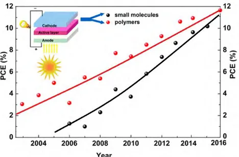
(PffBT4T-2OD). The power conversion efficiencies of BHJ architecture fabricated by blends of conjugated polymers and soluble fullerene derivatives have seen a dramatic rise from around 1% in 1992(39) to over 10% in 2013 - 2015(23, 25, 40, 93-99), as evidenced by the performance shown in Table I-1. High Jsc over 17.3 mA· cm-2 (94, 96, 146), high Voc over 1 V (147-149), and fill factor (FF) over 0.70 (94, 96) have been reported in different polymer-based BHJ devices. The combination of all these striking values should ultimately drive the efficiency to 12% and beyond in the near future in single junction PSCs. Particularly, so far the best PCE for single junction (BHJ) has reached 11.7%.(21) Typically, for tandem device, efficiencies over 11% have also been achieved, such as 11.3% for double junction (23), 11.5% for triple junction(25), and a new record of 13.2% set by Heliatek for multijunction (6).
(b) Small-molecules based donors
As succinctly illustrated in Figure I-24, solution-processed π-conjugated small molecules with narrow band gap have recently gained more attention for use as the donor component in BHJ solar cells with fullerene derivatives as electron acceptor materials. In regard to the performance in BHJ-OPVs, small molecules have almost caught up with their polymer counterparts.(19-21, 24, 29, 45, 84, 129, 130, 132, 137, 150)