Pour l'obtention du grade de
DOCTEUR DE L'UNIVERSITÉ DE POITIERS École nationale supérieure d'ingénieurs (Poitiers)
Laboratoire d'informatique et d'automatique pour les systèmes - LIAS (Diplôme National - Arrêté du 7 août 2006)
École doctorale : Sciences et ingénierie pour l'information, mathématiques - S2IM Secteur de recherche : Electronique, microélectronique et nanoélectronique
Cotutelle : Universitatea politehnica (Bucarest)
Présentée par :
Mihaela-Izabela Ionita
Contribution to the study of synchronized differential oscillators used to controm antenna arrays
Directeur(s) de Thèse :
Jean-Marie Paillot, David Cordeau, Mihai Iordache Soutenue le 18 octobre 2012 devant le jury
Jury :
Président Marina Topa Domnule Profesor, Universitatii tehnice din Cluj Napoca, Romania Rapporteur Farid Temcamani Professeur des Universités, ENSEA de Cergy-Pontoise
Rapporteur Lucian Mandache Domnule Profesor, Universitatea din Craiova, Romania Membre Jean-Marie Paillot Professeur des Universités, Université de Poitiers Membre David Cordeau Maître de conférences, Université de Poitiers
Membre Mihai Iordache Domnule Profesor, Universitatii Politehnice din Bucuresti, Romania
Pour citer cette thèse :
Mihaela-Izabela Ionita. Contribution to the study of synchronized differential oscillators used to controm antenna arrays [En ligne]. Thèse Electronique, microélectronique et nanoélectronique. Poitiers : Université de Poitiers, 2012. Disponible sur Internet <http://theses.univ-poitiers.fr>
THESE
en cotutelle
Pour l’obtention du Grade de
DOCTEUR DE L’UNIVERSITE DE POITIERS
(ECOLE SUPERIEURE d’INGENIEURS de POITIERS) (Diplôme National - Arrêté du 7 août 2006)
Ecole Doctorale : Sciences et Ingénierie pour l’Information et de
DOCTOR AL UNIVERSITATEA POLITEHNICA DIN BUCUREŞTI
Facultatea INGINERIE ELECTRICĂ Catedra de ELECTROTEHNICĂ
Secteur de Recherche : ELECTRONIQUE, MICROELECTRONIQUE ET NANOELECTRONIQUE
Présentée par :
MIHAELA-IZABELA IONITA
************************
CONTRIBUTION TO THE STUDY OF SYNCHRONIZED DIFFERENTIAL OSCILLATORS USED TO CONTROL ANTENNA ARRAYS
************************
Directeurs de Thèse : Jean-Marie PAILLOT, Mihai IORDACHE Co-directeur de Thèse : David CORDEAU
************************ Soutenue le 18 Octobre 2012 devant la Commission d’Examen
************************
JURY
Rapporteurs :
Farid TEMCAMANI Professeur à l’ENSEA de Cergy-Pontoise
Lucian MANDACHE Professeur à l’Université de Craiova Examinateurs :
Marina TOPA Professeur à l’Université technique de Cluj Napoca
Jean-Marie PAILLOT Professeur à l’Université de Poitiers
Mihai IORDACHE Professeur à l’Université Polytechnique de Bucarest
iii
ACKNOWLEDGEMENTS
First and foremost I want to thank my advisors Mr. Jean-Marie Paillot, Mr. David Cordeau, professors at University of Poitiers, France and Mr. Mihai Iordache, professor at University Politehnica of Bucharest. It has been an honor to work with you as a Ph.D. student. I appreciate all your contributions of time, ideas, and funding to make my Ph.D. experience productive and stimulating. I have learned so much from you, from figuring out what research is, to choosing a research agenda, to learning how to present my work. Your constructive criticism and collaboration have been tremendous assets throughout my Ph.D.
I would also like to thank the rest of my thesis committee for their support. Mr. Farid Temcamani, professor at University of Cergy-Pontoise, Mr. Lucian Mandache, professor at University of Craiova and Mrs. Marina Topa, professor at Technical University of Cluj-Napoca, which provided me invaluable advice and comments on both my research and my future research career plans. I would also like to thank to Mrs. Lucia Dumitriu, for her support and encouragements.
I’ve been very lucky throughout most of my life as a Ph.D student, in that I’ve been able to concentrate mostly on my research. This is due in a large part to the gracious support of the team from LAII (Laboratoire d’Automatique et d’Informatique Industrielle) of University of Poitiers, France. The team has been a source of friendships as well as good advice and collaboration. I am especially grateful to Mr. Smail Bachir and Mr. Claude Duvanaud, professors at University of Poitiers.
I would also like to express my thanks to the head of the LAII, Mr. Gerard Champenois, for accepting me as Ph. D student in his laboratory and for the funding sources that made my Ph.D. work possible in France.
I gratefully acknowledge the funding sources from University Politehnica of Bucharest and I would also like to express my thanks to prof.dr.ing. Ecaterina Andronescu.
I’ve been fortunate to have a great group of friends that became a part of my life. Not only are you the people I can discuss my research with and goof off with, but also you are confidants who I can discuss my troubles with and who stand by me through thick and thin. This, I believe, is the key to getting through a Ph.D. program – having good friends to have fun with and complain to.
iv
v
TABLE OF CONTENT
Introduction………..
1
Chapter I – Coupled-Oscillator Arrays – Application.…………..
4
1.1.
Introduction...………...
5
1.2.
Oscillator principle……...………...
6
1.2.1.
The sinusoidal oscillator………..
9
1.2.1.1.
The RC oscillator………...
10
1.2.1.2.
The LC oscillator………...
12
1.2.1.3.
Crystal oscillator………...
13
1.2.1.4.
The Armstrong oscillator………..
14
1.2.1.5.
The Hartley oscillator………
15
1.2.1.6.
The Colpitts oscillator………...
16
1.2.1.7.
The Pierce oscillator………..
16
1.2.1.8.
The differential oscillator………..
17
1.2.1.9.
The Van der Pol oscillator…...
19
1.3.
State of the art of coupled oscillators theory………..
20
1.4.
Applications: Beamsteering of antenna arrays………...
22
1.4.1.
Antenna arrays……….
23
1.4.1.1.
Uniform linear network………...
24
1.4.1.2.
Controlling the shape of the radiation
pattern………...
26
1.4.1.2.1.
Phase synthesis………..
27
1.4.1.2.2.
Amplitude and phase synthesis
31
1.4.2.
The control of the radiation pattern using coupled
oscillators……….
33
vi
2.1.
Introduction………..
37
2.2.
Dynamics of two Van der Pol oscillators coupled through a
resonant circuit……….
38
2.3.
Dynamics of two Van der Pol oscillators coupled through a
broad-band circuit………
48
2.4.
New formulation of the equations describing the locked states
of two Van der Pol coupled oscillators allowing a more
accurate prediction of the amplitudes………....
51
2.4.1.
Two Van der Pol oscillators coupled through a
resonant network……….
51
2.4.2.
Resistive coupling case………
60
2.5.
New formulation of the equations describing the locked states
of two Van der Pol oscillators allowing an easier numerical
solving method……….
61
2.6.
CAD tool “ASVAL”………....
68
2.6.1.
The objective of “ASVAL”……….
68
2.6.2.
Variables estimation technique………...
71
2.6.3.
Stability of synchronized states………..
72
2.7.
The cartography of the synchronization area……….
74
2.8.
Conclusion……….………..
77
Chapter III – Study and Analysis of an Array of Differential
Oscillators and VCOs Coupled Through a Resistive
Network………
79
3.1.
Introduction………..
80
3.2.
Analysis and design of two differential oscillators coupled
through a resistive network……….
81
3.2.1.
RLC differential oscillator schematic………….
81
3.2.2.
The modeling of the differential oscillator as a
84
vii
Van der Pol oscillator
3.2.2.1.
The modeling of the passive part…………..
84
3.2.2.2.
The modeling of the active part………
85
3.2.2.3.
Simulations of the Van der Pol oscillator….
87
3.2.3.
Two coupled differential Van der Pol oscillators..
88
3.2.4.
Two coupled differential oscillators………...
93
3.2.5.
Comparison between the theory, the Van der Pol
model and the differential structure………
96
3.2.6.
Study and analysis of the two coupled differential
oscillators in the weak coupling case………..
100
3.2.7.
Study and analysis of the two coupled differential
oscillators in the strong coupling case………
103
3.3.
Analysis and design of two VCOs coupled through a resistive
network…...………..
106
3.3.1.
Introduction………..
106
3.3.2.
The LC VCO architecture………
109
3.3.2.1.
The design of the passive part………...
110
3.3.2.2.
The design of the active part……….
111
3.3.2.3.
VCO simulation results……….
112
3.3.3.
The modeling of a differential VCO as a
differential Van der Pol oscillator………...
115
3.3.3.1.
The modeling of the passive part…………..
115
3.3.3.2.
The modeling of the active part………
117
3.3.4.
Two coupled differential VCOs………..
120
3.3.4.1.
Study and analysis of two coupled differential
VCOs of an optimal coupling case……….
120
3.3.4.1.1.
Study and analysis of two
coupled differential VCOs using the state
equation approach………..
125
3.3.4.2.
Study and analysis of two coupled differential
131
viii
3.3.4.3.
Study and analysis of two coupled differential
VCOs in the strong coupling case………
133
3.3.4.4.
Study and analysis of the variation of the phase
shift
∆φ
versus the coupling resistor R
c135
3.3.4.5.
The effect of a mismatch between the two R
con
the phase shift
∆φ
……….
138
3.3.5.
Four coupled differential VCOs………..
140
3.4.
Conclusion.………...
142
Final conclusion.….………..
144
List of publications………..
150
Appendix A………
151
Appendix B………
156
References……….
166
Abstract……….
173
x
No. fig.
Title of the figure
Page
Figure 1.1
Block diagram of an array of N coupled oscillators….
6
Figure 1.2
Linear model of an oscillator….………...
7
Figure 1.3
Model of a one-port oscillator..……….
8
Figure 1.4
The block diagram of a typical feedback amplifier...
10
Figure 1.5
The RC oscillator………..…..
10
Figure 1.6
The LC oscillator………..…..
12
Figure 1.7
Feedback signal coupling for the LC oscillators……...
13
Figure 1.8
The symbol and the equivalent circuit of a quartz
crystal………...
13
Figure 1.9
(a) Series-fed Armstrong oscillator; (b) Shunt fed
Armstrong oscillator………..
14
Figure 1.10
The Hartley oscillator…………...
15
Figure 1.11
The Colpitts oscillator………
16
Figure 1.12
A Pierce oscillator with PNP transistor in the
common-base configuration………...
17
Figure 1.13
Electronic structure of a differential oscillator……….
18
Figure 1.14
Electronic structure of a Van der Pol oscillator………
20
Figure 1.15
Linear network scheme………..………
25
Figure 1.16
The imposed sizes of the level and opening for the
main and side lobes………
27
Figure 1.17
The control on RF path……….……….
30
Figure 1.18
The
architecture
with
polyphase
oscillators
represented here with four antennas………..
30
Figure 1.19
The architecture with four coupled VCOs………
31
xi
Figure 1.21
Vector modulator architecture used on RF path.…….
32
Figure 1.22
Block diagram of an antenna array using coupled
oscillators………....
34
Figure 2.1
Two Van der Pol oscillators coupled through a RLC
circuit……….….
39
Figure 2.2
Van der Pol oscillator model………...…..
52
Figure 2.3
Two Van der Pol oscillators coupled through a series
RLC circuit………...………..
53
Figure 2.4
The graphical representation of a synchronization
area……...………...
70
Figure 2.5
Two coupled differential Van der Pol oscillators…….
75
Figure 2.6
The cartographies of the phase shift
∆φ
, the
amplitudes A
1and A
2and the synchronization
frequency f
Sof the coupled oscillators………
76
Figure 2.7
The cartography of the phase shift: example
∆φ
= 42°
77
Figure 3.1
The schematic of the RLC differential oscillator……..
81
Figure 3.2
a) The waveforms of the output voltage of the
differential oscillator; b) The output spectrum……….
83
Figure 3.3
The identification of the Van der Pol passive part
parameters………...
85
Figure 3.4
The Van der Pol characteristic………...
86
Figure 3.5
The differential Van der Pol oscillator model with i =
-av +bv
3………..
87
Figure 3.6
Comparison between the output voltages of the
differential oscillator and the differential Van der Pol
oscillator model………..
88
Figure 3.7
Two coupled Van der Pol oscillators……….
88
Figure 3.8.a
Two single-ended oscillators coupled through a
resistor……….
89
xii
∆
=7,4%; b) The output spectrum………...
92
Figure 3.10
Two differential oscillators coupled through a resistor
93
Figure 3.11
a) The waveforms of the output voltages of the
coupled differential oscillators for
∆
=7.4%; b) The
output spectrum………..
95
Figure 3.12
Cartography of the oscillators’ locked states provided
by the CAD tool………..
97
Figure 3.13
Waveforms of the output voltages of the two coupled
differential NMOS oscillators, when
∆φ
= 31.23° and
A = 2.72 V
98
Figure 3.14
a) Comparison of the phase shift; b) Comparison of
the amplitude………..
99
Figure 3.15
The weak coupling case – a) Comparison of the phase
shift; b) Comparison of the amplitude
101
Figure 3.16
The cartographies of the phase shift
∆φ
, the
amplitudes A
1and A
2and the synchronization
frequency f
sof the coupled oscillators for the weak
coupling case………..
103
Figure 3.17
The strong coupling case – a) Comparison of the
phase shift; b) Comparison of the amplitude…………
104
Figure 3.18
The cartographies of the phase shift
∆φ
, the
amplitudes A
1and A
2and the synchronization
frequency f
sof the coupled oscillators for the strong
coupling case………..
105
Figure 3.19
The RLC NMOS differential oscillator: a)Comparison
of
∆φ
while changing L and C; b) Comparison of the
amplitude while changing L and C………
107
Figure 3.20
The Van der Pol oscillator: a) Comparison of
∆φ
while changing L and C; b) Comparison of the
xiii
Figure 3.21
The LC VCO schematic……….
109
Figure 3.22
a) Variation of C versus Vtune; b) Variation of Q
versus Vtune………
111
Figure 3.23
The VCO oscillation frequency versus Vtune………...
112
Figure 3.24
The output power of the VCO………
113
Figure 3.25
The output voltages of the VCO………
113
Figure 3.26
Simulated phase noise of the VCO for a tuning
voltage of 0.62 V………
114
Figure 3.27
Simulated phase noise at 1 MHz versus tuning
voltage……….
114
Figure 3.28
The identification of the parameters of the Van der
Pol resonator………...
116
Figure 3.29
The real and imaginary part of the two impedances
Z
11and Z
22………...
117
Figure 3.30
The Van der Pol characteristic obtained for a VCO….
118
Figure 3.31
The differential output voltage of a VCO at 5.89 GHz
119
Figure 3.32
The differential Van der Pol oscillator………...
119
Figure 3.33
Two coupled differential VCOs……….
120
Figure 3.34
Two differential Van der Pol coupled oscillators…….
120
Figure 3.35
Cartography of the VCOs’ locked states provided by
the CAD tool………...
122
Figure 3.36
Waveforms of the output voltages of the two
differential NMOS VCOs for
∆φ
= 65.6° and A≈1.5 V
123
Figure 3.37
a) Comparison of the phase shift; b) Comparison of
the amplitude………..
124
Figure 3.38
Two differential Van der Pol oscillators coupled
through a resistor with G
NL= -a + bu
C12
(t)…………...
126
Figure 3.39
The output voltages of two coupled differential Van
der Pol oscillators obtained with Matlab for
∆φ
=
xiv
Figure 3.41
The weak coupling case – a) Comparison of the phase
shift; b) Comparison of the amplitude………...
132
Figure 3.42
The cartographies of the phase shift
∆φ
, the
amplitudes A
1and A
2and the synchronization
frequency f
sof the coupled VCOs for the weak
coupling case………..
133
Figure 3.43
The strong coupling case – a) Comparison of the
phase shift; b) Comparison of the amplitude…………
134
Figure 3.44
The cartographies of the phase shift
∆φ
, the
amplitudes A
1and A
2and the synchronization
frequency f
sof the coupled VCOs for the strong
coupling case………..
135
Figure 3.45
The variation of the phase shift versus R
cwhen f
0=
100 MHz……….
137
Figure 3.46
The variation of the phase shift versus R
cwhen f
0=
200 MHz……….
137
Figure 3.47
a) The variation of the phase shift for 5% mismatch;
b) The variation of the amplitude for 5% mismatch….
139
Figure 3.48
a) The variation of the phase shift for 7% mismatch;
b) The variation of the amplitude for 7% mismatch….
140
Figure 3.49
Schematic of four coupled VCOs………..
141
Figure 3.50
Waveforms of the output voltages of the four
xv
LIST OF TABLES
No. table
Title of the table
Page
Table 1
The synchronization frequency, phase shift and
amplitude obtained for two coupled differential Van
der Pol oscillators………...
91
Table 2
The synchronization frequency, phase shift and
amplitude obtained for two coupled differential
oscillators………
94
1
Introduction
2
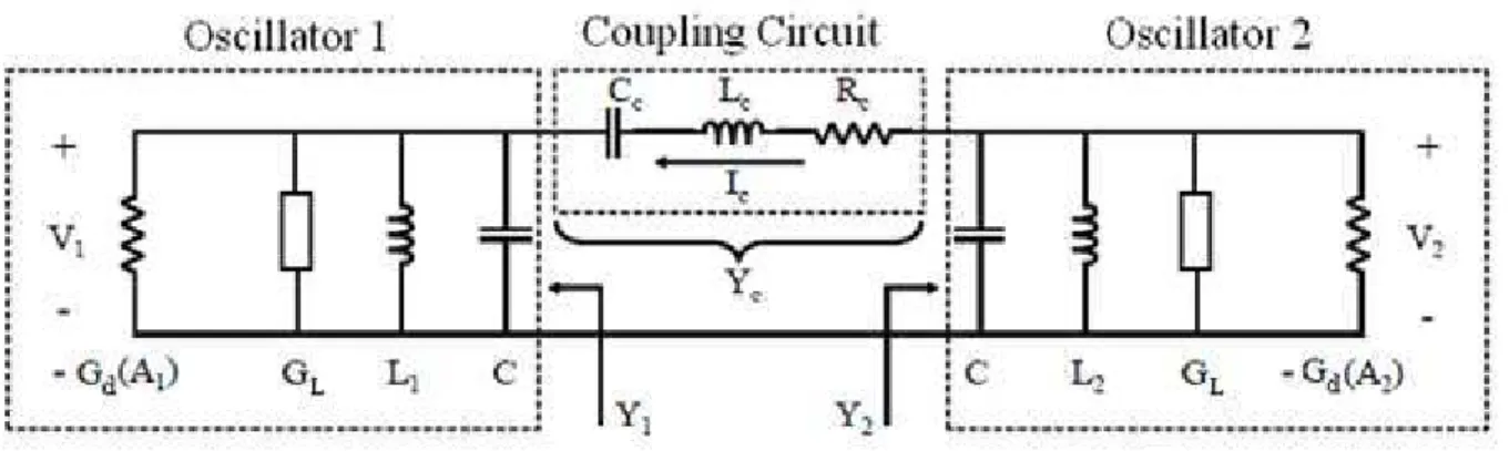
Arrays of coupled oscillators offer a potentially useful technique for producing higher powers at millimeter-wave frequencies with better efficiency than is possible with conventional power-combining techniques. Another application is the beam steering of antenna arrays. In this case, the radiation pattern of a phased antenna array is steered in a particular direction by establishing a constant phase progression in the oscillator chain which is obtained by detuning the free-running frequencies of the outermost oscillators in the array. Moreover, it is shown that the resulting inter-stage phase shift is independent of the number of oscillators in the array. Furthermore, synchronization phenomena in arrays of coupled oscillators are very important models to describe various higher-dimensional nonlinear phenomena in the field of natural science.
Many techniques have been used to analyse the behaviour of coupled oscillators for many years such as time domain approaches or frequency domain approaches. Concerning the last ones, R. York & al. made use of simple Van der Pol oscillators to model microwave oscillators coupled through either a resistive network or a broad-band network. Since these works are limited to cases where the coupling network bandwidth is much greater than the oscillators’ bandwidth, he used more accurate approximations based on a generalization of Kurokawa’s method to extend the study to the case of a narrow-band circuit. This theory allows the equations for the amplitude and phase dynamics of two oscillators coupled through many types of circuits to be derived. As a consequence, it provides a full analytical formulation allowing to predict the performances of microwave oscillator arrays. Unfortunately, it is shown that the theoretical limit of the phase shift that can be obtained by slightly detuning the end elements of the array by equal amounts but in opposite directions is only ±90°. Thus, it seems interesting to study and analyze the behavior of an array of coupled differential oscillators or Voltage Controlled Oscillators (VCOs) since, in this case, the theoretical limit of the phase shift is within 360° due to the differential operation of the array, leading to an efficient beam-scanning architecture for example. Furthermore, differential oscillators are widely used in high-frequency circuit design due to their relatively good phase noise performances and ease of integration.
Due to these considerations, the aim of this work is to study and analyze the behavior of coupled differential oscillators and VCOs used to control antenna arrays.
3
In the first chapter, we will first remind the principle of an oscillator, including the Van der Pol oscillator. Then, a state of the art of coupled-oscillator theory will be provided followed by a brief presentation of antenna arrays theory and their applications in the communication systems. Finally, few technical solutions to control the radiation pattern will be presented, including the coupled oscillators approach.
In chapter 2, an overview over R. York’s theory giving the dynamics for two Van der Pol oscillators coupled through a resonant network will be presented. Then, the case of a broadband coupling circuit will be showed. Since the Van der Pol model used is too simple and doesn’t allow an accurate prediction of the amplitudes, a new formulation of the equations describing the locked states of these two coupled oscillators using an accurate model allowing a good prediction of the amplitudes will be then described. Finally, mathematical manipulations will be applied to the dynamic equations describing the locked states of the coupled Van der Pol oscillators. A reduced system of equations with no trigonometric aspects will be obtained, leading to the elaboration of a CAD tool that provides, in a considerably short simulation time, the frequency locking region of two differential oscillators coupled through a resistive network, in terms of the amplitudes of their output signals and the phase shift between them.
The last chapter will be dedicated to the study and the analysis of an array of differential oscillators and VCOs coupled through a broadband network. Hence, in the first part of this chapter dealing with the analysis of two coupled differential oscillators, a modeling procedure of the differential oscillator as a differential Van der Pol oscillator will be presented. Then, the proposed CAD tool will be used in order to obtain the cartography of the oscillators’ locked-states. The validation of the results provided by our CAD tool will be showed by comparing them to the simulation results of the two coupled differential oscillators obtained with Agilent’s ADS software for different cases of coupling strength. Then, the same study will be performed for the case of two coupled differential Voltage Controlled Oscillators (VCOs). Furthermore, the study of the variation of the phase shift versus the coupling resistor will also be investigated as well as the effect of a mismatch between the two coupling resistors on the phase shift. Finally, the behavior of four coupled differential VCOs will be presented.
4
CHAPTER I
5
1.1.
INTRODUCTION
During the past decade, arrays of coupled oscillators are the subject of increasing research activity due to successful modeling of many diverse biological and physical phenomena. Biological examples include swarms of synchronously flashing fireflies, the coordinated firing of cardiac pacemaker cells, rhythmic spinal locomotion in vertebrates and the synchronized activity of nerve cells in response to external stimuli. In physical sciences, examples include oscillations in certain nonlinear chemical reactions, the collective behavior of Josephson junction arrays and laser diode arrays [1]. Almost any system of discrete or distinguishable behavior can be modeled by a system of coupled oscillators.
In electronics, in particular, the synchronization behavior of oscillators has been exploited in many relevant applications. Frequency locking effects have been used to realize low-cost high-performance quadrature oscillators [2] or to reduce the effect of noise [3]. Injection locking is the principle, which is at the basis of phase-locked loops (PLL) circuits, furthermore it is employed to realize low-power consumption frequency dividers for high-frequency applications [4]. Moreover, arrays of coupled oscillators offer a potentially useful technique for producing higher powers at millimeter-wave frequencies with better efficiency than is possible with conventional power-combining techniques [5, 6]. Another application is the beam steering of antenna arrays [7]. In this case, the radiation pattern of a phased antenna array is steered in a particular direction by establishing a constant phase progression in the oscillator chain. For a linear array presented in Figure 1.1, a phase shift ∆φ between adjacent elements results in steering the beam to an angle θ off broadside, which is given by:
φ ∆ π λ = θ d arcsin 2 0 , (1.1)
where d is the distance separating two antennas and λ0 is the free-space wavelength
[8]. The required inter-stage phase shift can be obtained by detuning the free-running frequencies of the outermost oscillators in the array [9, 10]. Moreover, it is shown that the
Chapter I – Coupled-Oscillator Arrays - Application
6
resulting inter-stage phase shift is independent of the number of oscillators in the array [1, 11, 12].
Figure 1.1 – Block diagram of an array of N coupled oscillators
In this chapter we will first remind the principle of an oscillator, where different types of sinusoidal oscillators will be presented including the differential and Van der Pol oscillators. Then, a state of art of coupled-oscillator theory will be provided followed by a brief presentation of antenna arrays theory and their applications in the communication system. Finally, few technical solutions to control the radiation pattern will be presented, including the coupled oscillators approach.
1.2.
OSCILLATOR PRINCIPLE
An oscillator is usually represented as a closed loop system. In Figure 1.2, we can see a linear model of an oscillator, where A(jω) represents the transfer function of the active element of the oscillator, and B(jω) represents the transfer function of the passive part of the reaction, which gives the selection and stability of the oscillation frequency. This passive part is represented by the resonator.
7
Figure 1.2 - Linear model of an oscillator.
The transfer function of this system can be written as follows:
ω) ω 1 ω ω ω ) B ( j - A ( j ) A ( j ) ( j V ) ( j V e s = . (1.2)
Considering this expression, there is a pulsation, ω0, for which: Vs(jω0) ≠ 0 whereas
Ve(jω0) = 0; this pulsation must fulfill the relation A(jω0) .B(jω0) = 1.
Therefore, the oscillation conditions, known as Barkhausen, are written as follows:
= = π 2 ω ω 1 ω ω 0 0 0 0 k ) ) .B ( j j Arg ( A ( ) ) .B ( j A ( j (1.3) where k ∈ N.
Therefore, in steady state, the module of the opened loop gain must be equal to one and the total phase shift must be zero or 2kπ.
An oscillator circuit can also be represented by a nonlinear impedance, ZNL(I, ω),
which represents the active part of the oscillator, in parallel with the equivalent impedance of the resonator, ZR(ω), as shown in Figure 1.3.
Chapter I – Coupled-Oscillator Arrays - Application
8
Figure 1.3 – Model of a one-port oscillator.
In these conditions, Kirchoff laws give:
(ZNL ( I,ω0) + ZR (ω0)) .I = 0, (1.4)
In order to obtain an oscillation phenomena with i(t) = I cos(ω0t), the oscillation
condition becomes:
ZT (I, ω0) = ZNL (I, ω0) + ZR (ω0) = 0. (1.5)
This condition can be expressed in terms of real parts, RT, and imaginary part, XT, of
the total impedance ZT, so that:
RT ( I, ω0) = 0, (1.6)
XT ( I, ω0) = 0. (1.7)
These two equations give the condition for the sustaining of the oscillations and the oscillation frequency of the circuit. As the real part of the equivalent impedance of the passive part is positive at the pulsation ω0, the condition for sustaining the oscillation,
defined by equation (1.6) can be fulfilled only if the real part of the non-linear impedance is negative at the pulsation ω0, which can be obtained by an active element.
9
Oscillators are classified in accordance with the waveforms they produce and the circuitry required for producing the desired oscillations, as presented in [13]:
The sinusoidal oscillator - the output voltage is sinusoidal;
The non-sinusoidal oscillator - the output voltage is non-sinusoidal but it has triangular, square and saw tooth waveforms.
1.2.1.
The Sinusoidal Oscillator
A sinusoidal oscillator is an oscillator that produces a sine-wave output signal. An ideal oscillator should produce an output signal with constant amplitude with no variation in frequency. A practical oscillator cannot have these criteria, the degree to which the ideal is approached depends on the class of amplifier operation, amplifier characteristics, frequency stability, and amplitude stability. Sinusoidal oscillators generate signals ranging from low audio frequencies to ultrahigh radio and microwave frequencies.
The sinusoidal oscillators are classified as follows:
• RC oscillators;
• LC oscillators;
• the crystal-controlled oscillator.
Many low-frequency oscillators use resistors and capacitors to form their frequency-determining networks and are referred to as RC oscillators. These are used in the audio-frequency range.
The LC oscillators are commonly used for the higher radio frequencies. They are not suitable for use as extremely low-frequency oscillators because the inductors and capacitors would be large in size, heavy, and costly to manufacture.
The third category of sinusoidal oscillator is the crystal-controlled oscillator. The crystal-controlled oscillator provides excellent frequency stability and is used from the middle of the audio range through the radio frequency range.
Chapter I – Coupled-Oscillator Arrays - Application
10
An oscillator must provide amplification where the amplification of signal power occurs from the input to the output of the oscillator and a portion of the output is feedback to the input to sustain a constant input.
Figure 1.4 represents the block diagram of a typical feedback amplifier, where:
• A – is the open-loop gain of the amplifier and Vout = AV;
• β – is the feedback factor and Vf = β Vout .
Figure 1.4 – The block diagram of a typical feedback amplifier.
If V = Vin – Vf, the feedback is negative and the amplifier is provided with negative
feedback. If V = Vin + Vf, the feedback is positive and the amplifier is provided with
positive feedback. As a consequence, the general expression for a feedback loop is as follows: A A V V A in out f β 1± = = , (1.8)
where βA is the loop gain, and 1±βA is the amount of feedback.
Practically, all amplifiers use negative feedback, but the sinusoidal oscillators use positive feedback.
1.2.1.1.
The RC Oscillator
11
Figure 1.5 – The RC oscillator.
This oscillator is composed of a RC network and an amplifier. This oscillator is also well-known as phase-shift oscillator. Theoretically, to satisfy the Barkhausen criterion and to sustain oscillations, both gain and phase conditions must be fulfilled. The bipolar transistor provides the amplification to achieve an open loop gain greater than one required for the start-up of the oscillation phenomena:
|β(jω0)A(jω0)| ≥ 1.
This structure is in a common-emitter configuration and then the phase shift is close to 180°. In these conditions, the passive part must present a phase shift greater than 180° at the oscillation frequency ω0. To obtain such a phase shift with RC components, a transfer
function presenting three poles is required. This implies the three RC network. The output of the oscillator contains only a single sinusoidal frequency. When the oscillator is powered on, the loop gain βA is greater than unity and the amplitude of the oscillations will increase. A level is reached when the gain of the amplifier decreases, and the value of the loop gain decreases to unity and constant amplitude oscillations are sustained. The frequency of oscillations is determined by the values of resistance and capacitance in the three sections. Variable resistors and capacitors are usually used to provide tuning in the feedback network for variations in phase shift.
Let us consider that the resistors R and Rb are greater than the input bipolar transistor impedance h11. In these conditions, for the RC oscillator of Figure 1.5, the
Chapter I – Coupled-Oscillator Arrays - Application
12 R R RC o L 4 6 1 + = ω (1.9)In general, for an RC phase-shift oscillator, the frequency of oscillation (resonant frequency) can be approximated with the following relation:
n RC 2
1
ω0 = , (1.10)
where n is the number of RC sections.
1.2.1.2.
The LC Oscillator
The LC oscillators use resonant circuits. A resonant circuit stores energy alternately in the inductor and capacitor. However, every circuit contains some resistance and this resistance causes reduction in the amplitude of the oscillations. Figure 1.6 shows a typical diagram of an LC oscillator.
Figure 1.6 – The LC oscillator.
In an LC oscillator the sinusoidal signal is generated by the action of an inductor and a capacitor. The feedback signal is coupled from the LC tank of the oscillator circuit by using a coil tickler or a coil pair as shown in Figure 1.7(a) and 1.7(b) or by using a
13
capacitor pair in the tank circuit as shown in Figure 1.7(c). A tickler coil is an inductor that is inductively coupled to the inductor of the LC tank circuit.
Figure 1.7 - Feedback signal coupling for the LC oscillators.
1.2.1.3.
Crystal Oscillator
Crystal oscillators are oscillators where the primary frequency determining element is a quartz crystal. Because of the inherent characteristics of the quartz crystal the crystal oscillator may be held to extreme accuracy of frequency stability. The frequency depends almost entirely on the thickness where the thinner the thickness, the higher the frequency of oscillation.
The symbol and the equivalent circuit of a quartz crystal are shown in Figure 1.8, where capacitor C1 represents the electrostatic capacitance between the electrodes of the
crystal and in general C1»C2.
Chapter I – Coupled-Oscillator Arrays - Application
14
The available power is limited by the heat the crystal will withstand without fracturing. The amount of heating is dependent upon the amount of current that can safely pass through a crystal and this current may be in the order of 50 to 200 milliamperes. Accordingly, temperature compensation must be applied to crystal oscillators to improve thermal stability of the crystal oscillator.
Crystal oscillators are used in applications where frequency accuracy and stability are of outmost importance such as broadcast transmitters and radar. The frequency stability of crystal-controlled oscillators depends on the quality factor Q. The Q of a crystal may vary from 10,000 to 100,000.
1.2.1.4.
The Armstrong Oscillator
In an Armstrong oscillator, the feedback is provided through a tickler coil. There are two types of Armstrong oscillator:
• series-fed tuned-collector Armstrong oscillator
• shunt-fed tuned-collector Armstrong oscillator
Figure 1.9 shows the two circuits known as Armstrong oscillators.
(a) (b)
15
The series-fed tuned-collector Armstrong oscillator is so-called because the power supply voltage Vcc supplied to the transistor is through the tank circuit. The shunt-fed
tuned-collector Armstrong oscillator is so-called because the power supply voltage Vcc
supplied to the transistor is through a path parallel to the tank circuit.
For both types of Armstrong oscillators, the power through Vcc is supplied to the
transistor and the tank circuit begins to oscillate.
The transistor conducts for a short period of time and returns sufficient energy to the tank circuit to ensure a constant amplitude output signal.
1.2.1.5.
The Hartley Oscillator
The Hartley oscillator is an improvement over the Armstrong oscillator. Although its frequency stability is not the best possible of all the oscillators, the Hartley oscillator can generate a wide range of frequencies and is very easy to tune. Such a type of oscillator is shown in Figure 1.10.
Figure 1.10 – The Hartley oscillator.
The main difference between the Armstrong and the Hartley oscillators lies in the design of the feedback (tickler) coil. A separate coil is not used. Instead, in the Hartley oscillator, the coil in the tank circuit is a split inductor. Current flow through one section induces a voltage in the other section to develop a feedback signal.
Chapter I – Coupled-Oscillator Arrays - Application
16
1.2.1.6.
The Colpitts Oscillator
Figure 1.11 shows a simplified version of the Colpitts oscillator.
Figure 1.11 – The Colpitts oscillator.
In a Colpitts oscillator the feedback is provided through a capacitor pair. The Colpitts oscillator provides better frequency stability than the Armstrong and Hartley oscillators. Moreover, the Colpitts oscillator is easier to tune and thus can be used for a wide range of frequencies.
For the oscillator circuit of Figure 1.11 the frequency of oscillation is as follows:
2 1 2 1 0 ω C LC C C + = , (1.11)
1.2.1.7.
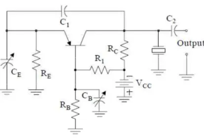
The Pierce Oscillator
Figure 1.12 shows a Pierce oscillator with a PNP transistor as an amplifier in the common-base configuration.
17
Figure 1.12 – A Pierce oscillator with PNP transistor in the common-base configuration.
The Pierce oscillator is a modified Colpitts oscillator that uses a crystal as a parallel-resonant circuit and for this reason is often referred to as crystal-controlled Pierce oscillator.
In the oscillator circuit of Figure 1.12, feedback is provided from the collector to the emitter of the transistor through capacitor C1 and resistors R1, RB, and RC are used to
establish the proper bias conditions. Besides the crystal, the frequency of oscillation is also determined by the settings of the variable capacitors CE and CB.
1.2.1.8.
The differential oscillator
Like the previous architectures, this type of oscillator presents a structure that resonates at a frequency for which the losses are compensated by the active part, [14]. Thus, this resistance Rp is in parallel with a structure that can present a negative resistance.
In steady state, to sustain the oscillation, the negative resistance must be equal to the losses resistance of the resonator. Usually, the negative resistance is represented by an element or an active circuit (a structure based on transistors), as shown in Figure 1.13.
Chapter I – C
The small-signal ana conductance between points a single transistor.
Figure 1.13 –
Thus, to ensure the provided by the pair of trans so that:
In steady state, the tr This implies that the losses r
Coupled-Oscillator Arrays - Appli
18
voutput = vx – vy.
analysis of the pair of transistors shows ts vx and vy is equal to
-2 m
g
where gm is the
Electronic structure of a differential osc
he start-up condition of the oscillator, th ansistors,
2 m
g
, must be greater than the losse
p m
R g > 2 .
transistor’s operating point varies from blo s resistance Rp is canceled by gm :
plication
(1.12)
s that the equivalent the transconductance of scillator. the transconductance sses conductance p R 1 , (1.13) blocking to saturation.
19
p m
R
g = − 1 . (1.14)
The problem of oscillation start-up is a critical problem in oscillators design. Equations (1.13) and (1.14) indicate that the transistors must be oversized. Moreover, because we can’t know precisely Rp, generally, the transistors have their transconductance
three or four times greater than that required in steady state.
The amplitude of the output voltage for this type of oscillator can be calculated according to the limits of the transistor’s operating point. If one transistor of the differential pair is off and the other is saturated, then, all the current IDC is flowing in this
latter. In this case we have:
= − = DC p y DD DD x I R v V V v 2 . (1.15)
And the amplitude is:
DC p y x I R v v A 2 = − = . (1.16)
1.2.1.9.
The Van der Pol oscillator
The Van der Pol oscillator is an oscillator with nonlinear damping governed by the second-order differential equation:
0 1 ε − 2 + = − ( x )x x x , (1.17) where:
Chapter I – Coupled-Oscillator Arrays - Application
20
• x- is the dynamical variable.
The Van der Pol model commonly used is made of a nonlinear conductance and a resonator, as shown in Figure 1.14. The general expression of the nonlinear conductance of the Van der Pol model is written as follows:
2 γ α V - GNL = + , (1.18) where:
• −α - is the negative conductance necessary to start the oscillation;
• 2
γV - is the nonlinear conductance which modelises the saturation phenomenon.
Figure 1.14 – Electronic structure of a Van der Pol oscillator.
1.3.
STATE OF THE ART OF COUPLED OSCILLATORS THEORY
Many techniques have been used to analyze the behavior of coupled oscillators for many years such as time domain approaches and frequency domain approaches. Concerning the frequency domain approaches, B. Van der Pol [15] started to study the oscillators’ synchronization phenomenon using an "averaging" method to obtain approximate solutions for quasi-sinusoidal systems. Then, R. Adler gave to the microwave
21
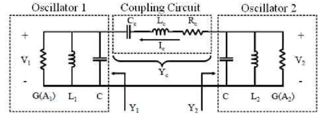
oscillator analysis a more physical basis defining the phase dynamic equation of an oscillator under the influence of an injected signal [16]. This was sustained by K. Kurokawa who derived the dynamic equations for both the amplitude and phase [17], providing a pragmatic understanding of coupled microwave oscillators. In R. York’s previous works, coupled microwave oscillators have been modeled as simple single-ended Van der Pol oscillators coupled through either a resistive network or a broad-band network [1, 11, 18]. Unfortunately, this works are limited to the cases when the coupling network bandwidth is much greater than the oscillators’ bandwidth. In these conditions, a generalization of Kurokawa’s method [17] was used to extend the study to a narrow-band circuit allowing the equations for the amplitude and phase dynamics of two oscillators coupled through many types of circuits to be derived [19]. Since these works, only few papers present new techniques for the analysis of coupled-oscillator arrays in the frequency domain [20, 21, 22]. In [22], a semi-analytical formulation is presented for the design of coupled oscillator systems, avoiding the computational expensiveness of a full harmonic balance synthesis presented in [20] and [21]. In [23], a simplified closed-form of the semi-analytical formulation proposed in [22] for the optimized design of coupled-oscillator systems is presented. Nevertheless, even if this new semi-analytical formulation allows a good prediction of the coupled oscillator solution, it is only valid for the weak coupling case.
Now, concerning the time domain approaches [24-29], among other, D. Aoun and D.A. Linkens studied in [24] nonlinear oscillators used in bioelectronics applications, in particular, towards the electrical activity of the mammalian gastro-intestinal tract. This activity known as “slow-waves” has been extensively modeled using nonlinear oscillatory dynamics. Therefore, they applied a matrix extension of the Krylov-Bogolioubov linearization technique to a wide range of structures comprising chains, arrays, rings and tubes. Unfortunately, it has been demonstrated that this technique produces complicated stability criteria for the existence of stable limit cycles. Hence, they decided to engineer a CAD package which solves these criteria for the structures mentioned above with an arbitrary number of either third or fifth power conductance Van der Pol oscillators coupled mutually. Later on, Chai Wah Wu and Leon O. Chua demonstrated in [25] how an array of resistively coupled identical oscillators can be synchronized if the coupling conductances
Chapter I – Coupled-Oscillator Arrays - Application
22
are large enough. To do so, they used algebraic graph theory to derive sufficient conditions for an array of resistively coupled nonlinear oscillators to synchronize. These conditions are derived, in fact, from the connectivity graph, which describes how the oscillators are connected. Moreover, they showed that the upper bound on the coupling conductance required for synchronization for arbitrary graphs, is in order of n2, where n is the number of oscillators. In [26], P. Maffezoni studies the synchronization phenomenon of the weakly coupled oscillators using a phase-domain macromodel based on perturbation projection vector that describes the linear periodically time-varying behavior of an oscillator in the neighbor of its stable limit cycle. Using this method, the mutual locking range and the common locking frequency of the locked oscillators could be predicted with great precision. The reliability and accuracy of the method have been demonstrated also when the mutual coupling results in an anomalous synchronization frequency. Furthermore, in this way Maffezoni could estimate, by means of closed-form expressions, the mutual pulling effects that arise between two self-sustained oscillators in the presence of weak interactions.
Nevertheless, even if the time domain approaches offer a good prediction of the coupled oscillator solution, the frequency domain approaches are less complex and more preferred in the design of RF and microwave coupled oscillators. For instance, R. York’s theory [19] provides a full analytical formulation allowing to predict the performances of microwave oscillator arrays for both weak and strong coupling.
1.4.
APPLICATIONS: BEAMSTEERING OF ANTENNA ARRAYS
Mobile communications are the subject of increasing research activity covering many technical areas. Worldwide activities in this growing industry are perhaps an indication of its importance.
An application of antenna arrays has been suggested in the recent years for mobile communication systems in order to solve the problem of limited bandwidth of the channel, and therefore, to satisfy the increasing demands for a large number of mobile communication channels [30, 31]. Antenna arrays have many other advantages, in fact,
23
they contribute to the improving of the communication system performances while increasing the channel capacity, providing a wider band of coverage, and minimizing the multipath fading and also the interference between channels. Beside the advantages mentioned in this paragraph, the two properties below also describe a few assets of antenna arrays:
− The decrease of the electromagnetic pollution: the shape of the radiation pattern can be optimized in order to reduce the side lobes. Similarly, the radiation pattern can be orientated in the desired direction, and therefore any radiations in useless directions are minimized.
− A better quality of the transmission / reception: the emitted power can be focused in the desired direction and therefore the wasted power in useless directions is reduced. One of the advantages resulting from this decrease is also the distribution of the power on all power amplifiers constituting the transmission network. Similarly, for the reception, the noise provided by the interfering signals is minimized, leading to a reduced Bit Error Rate (BER), which is the priority of any transmission architecture.
Thus, antenna arrays are essential to increase the efficiency of mobile communications systems. For the transport area, these devices are installed on vehicles, boats, planes, satellites and base stations in order to fulfill the channel requirements for this service.
1.4.1.
Antenna Arrays
An antenna array is defined as a set of N radiating elements distributed in space. The amplitude and/or phase of the signal injected into each of these antennas can be commanded so that it can control the shape of the radiation pattern of the network as well as its orientation. These commands can be chosen so that several lobes can be created simultaneously or a single lobe in the direction of the incident signal and zero in the direction of the interference wave.
Chapter I – Coupled-Oscillator Arrays - Application
24
The main characteristics of an antenna array are determined by the number and type of antennas constituting the network and also their geometric arrangement.
For reasons of simplicity and implementing, identical elements are chosen. An antenna array has the following possible configurations:
• Linear - antennas are aligned in a straight line;
• Circular - the antennas are arranged in a circle;
• Planar - the antennas are arranged on a plane;
• Surface - the antennas are arranged on a surface with a curvature, such as a sphere or a cylinder;
• Volume - the antennas are distributed in a volume.
1.4.1.1.
Uniform linear network
The radiation pattern of an antenna array is based on basic physical structure of antennas and network geometry, but also on their command signals [32]. When the basic sources of a linear network are excited with the same amplitude, the linear network is considered to be uniform, and therefore is called equi-amplitude.
We consider a uniform network of N elements identical and equidistant with a distance d between them along an axis x, commanded by N sources with a phase gradient
φ
∆ , one against another. This network is illustrated in Figure 1.15, where r is the maximum distance between reference antenna and the observation plane, and θ is the angle of the main lobe direction.
25
Figure 1.15 - Linear network scheme.
In these conditions, in far field, the total electrical field radiated by an antenna array is: ) ( A E Etot = 0 × ψ , (1.19) where:
• E0 - is the electrical field radiated by an elementary antenna. It's called “element factor” and depends only on the physical characteristics of the elementary antenna;
• A(ψ) – is the “array factor” and depends on the geometry of the network and on the
size of the amplitude and phase applied to the network elements. This array factor has the following formula:
) ( sin ) N ( sin ) / ) ( j ( N -exp N ) A ( 2 2 2 ψ 1 1 ψ ψ = ψ , (1.20) where θ ∆φ λ π =
Chapter I – Coupled-Oscillator Arrays - Application
26
The total radiation pattern of the antenna array is then defined by the product of the module of the electric field radiated by an elementary antenna by the array factor, which is given by the following expression:
) ( sin ) N ( sin N ) A ( 2 2 1 ψ ψ = ψ . (1.21)
Under these conditions, it is important to observe that when the number N of elementary antennas is increased, the total radiation pattern of the network depends more on the array factor and less on the radiation pattern of each elementary antenna.
1.4.1.2.
Controlling the shape of the radiation pattern
The main purpose of an array of N radiating elements is to control the distribution of the energy radiated or received in the space. This control is based on the establishment of an appropriate control law. This is possible by applying the optimal values of the amplitudes and / or phases to the signals injected into each elementary antenna of the array. Thus, the synthesis of the radiation pattern of an antenna array consists in determining the set of parameters of the control law able to produce a radiation pattern which meets all the required elements.
The characteristics of the radiation pattern of an array are determined by the level and / or the opening of the side lobes compared to those of the main lobe, as shown in Figure 1.16. Thus, more the opening of the latter decreases, the level of the side lobes increases, and therefore, a significant part of the power is “wasted”. In these conditions, it is necessary to model the radiation pattern in order to obtain the lowest level of the side lobes so that the required opening of the main lobe is obtained and the losses induced in other directions are minimized.
27
Figure 1.16 – The imposed sizes of the level and opening for the main and side lobes.
Due to these considerations, three synthesis solutions can be envisaged. The first is to synthesize only the amplitude. This technique yields the direction lobes with the possibility of controlling the level of the side lobes. The coefficients of the array can be calculated using analytical techniques developed among others by Fourier or Chebyshev. However, applications of this type of synthesis are limited. Thus, this solution is not studied in detail in this manuscript. The other two solutions are presented in the following.
1.4.1.2.1.
Phase synthesis
This solution allows to perform beam-steering of the antenna array. To do so, several solutions with phase shifters or phase shifterless can be used as described below:
• A first approach illustrated in Figure 1.17 is relatively well known. The intermediate frequency IF of the signal is converted in a RF frequency thanks to the oscillator
LO. The resulting signal is then divided using power dividers. Each of the obtained
signals is then amplified and phase shifted before being sent to the antenna elements of the array. The concept of this approach is simple, but these devices can introduce significant losses and a significant production cost. Moreover, the phase shifters are
Chapter I – Coupled-Oscillator Arrays - Application
28
passive devices difficult to integrate, and therefore their use in hybrid circuits is limited.
• Furthermore, in the area of passive beam distributors, two classes coexist [33]: 1- The quasi-optical types: they imply a hybrid arrangement meaning either a
reflector or a lens objective with an antenna array. The quasi-optical type which is the best known is the Rotman lens [34] which is a time delay device having the synthesis procedure based on the optical geometry principles. The input or output ports drive the cavity of a lens whose periphery is well defined. The excitation of an input port produces a uniform amplitude distribution and a linear phase gradient (constant) at the output ports. The Rotman lens is interesting because it allows a certain freedom of design with many parameters to adjust, one can obtain many beams with a stable frequency system. However, its disadvantages are not negligible, especially regarding the complexity of the design due to the number of variables to adjust and the mutual coupling between its ports.
2- The circuits’ types using the microstrip technology, striplines or waveguides such as the Butler matrix [35] which is a symmetrical passive mutual circuit with
N input ports and N output ports. This circuit drives N radiating elements
producing N different orthogonal beams. This is a parallel system made of junctions which connect the input ports to the output ports through equal length transmission lines. Thus, an input signal is many times divided without losses until the output ports. Despite its simple and lossless architecture, the Butler matrix has many disadvantages particularly regarding the number of components which increases considerably with the number of desired beams.
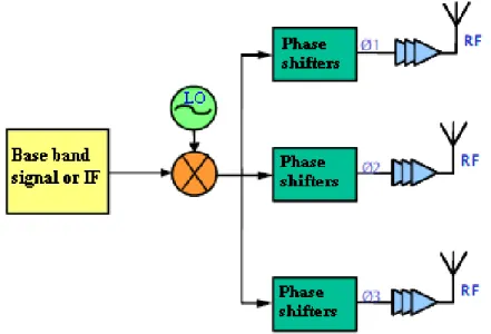
• Another approach illustrated in Figure 1.18, consists in using a polyphase voltage-controlled oscillator, which is able to generate the local oscillator frequency with N phases. In this architecture, all the N phases are conveyed to each antenna via a distribution network. Phase selectors ensure the required phase to each element [36, 37]. In this case, the phase variations are discrete, which does not constitute a problem as long as the discrimination steps are adequate to the application.
29
Nevertheless, the distribution network of N phases constitutes a real issue here since each path must be forwarded to the phase selector in a symmetrical way [38].
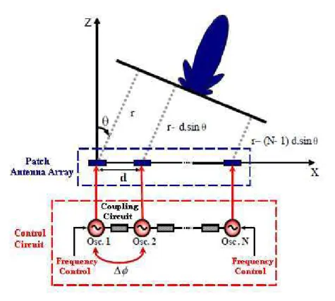
• An alternative approach consists in using an array of coupled voltage controlled oscillators as shown in Figure 1.19. When working, all the VCOs are synchronized at a common frequency and have different phases according to their free-running frequencies. In these conditions, the same phase difference is obtained between each pair of neighboring oscillators. Therefore, the control of the oscillation frequencies can impose the required phase shift and thus the desired radiation direction. This solution presents the advantage of providing a continuous variation of the phase shift, at the expense of the complexity of implementation. With this technique, it is difficult to control precisely the synchronization frequency, but this approach is very interesting especially for radar applications where it is important to control the orientation of the main lobe of the radiation pattern of the antenna array [11]. Nevertheless, uncertainties on the received frequency can be tolerated. Several methods can be applied to obtain the desired phase shift:
• By coupling the oscillators through delay lines as P. Liao and R. York proposed in [9].
• By changing the free running frequency of all the VCOs of the array as T. Heath demonstrated in [39]. Indeed, changing the free running frequencies of all the VCOs of the array, leads to a phase difference between the output voltages of the VCOs.
• By changing the free running frequencies of the two outermost VCOs of the array [40]. In these conditions, the same phase difference is obtained between each pair of neighboring oscillators. This third approach is discussed in detail later in this chapter.
Chapter I – Coupled-Oscillator Arrays - Application
30
Figure 1.17 – The control on RF path.
Figure 1.18 – The architecture with polyphase oscillators represented here with four antennas.
31
Figure 1.19 – The architecture with four coupled VCOs.
1.4.1.2.2.
Amplitude and phase synthesis
This solution allows to perform beamforming of the linear antenna array. This type of synthesis is efficient for applications of adaptive arrays but its implementation requires a control architecture in amplitude and phase, which involves a costly and complicated technique.
To do so, an active solution using vector modulators on LO path (Figure 1.20) or on
RF path (Figure 1.21) can be used. The main advantage of this architecture is on one hand
the simplicity of implementation (no distribution path of the complex phases) plus the stability of the frequency obtained by a frequency synthesizer, and on the other hand the control of the amplitude [38].
Chapter I – Coupled-Oscillator Arrays - Application
32
Figure 1.20 – Vector modulator architecture used on LO path.