HAL Id: hal-00480174
https://hal.archives-ouvertes.fr/hal-00480174
Submitted on 3 May 2010HAL is a multi-disciplinary open access
archive for the deposit and dissemination of sci-entific research documents, whether they are pub-lished or not. The documents may come from teaching and research institutions in France or abroad, or from public or private research centers.
L’archive ouverte pluridisciplinaire HAL, est destinée au dépôt et à la diffusion de documents scientifiques de niveau recherche, publiés ou non, émanant des établissements d’enseignement et de recherche français ou étrangers, des laboratoires publics ou privés.
Hexagonal and honeycomb structures in Dielectric
Barrier Discharges
B. Bernecker, T. Callegari, Stéphane Blanco, Richard Fournier, Jean-Pierre
Boeuf
To cite this version:
B. Bernecker, T. Callegari, Stéphane Blanco, Richard Fournier, Jean-Pierre Boeuf. Hexagonal and honeycomb structures in Dielectric Barrier Discharges. European Physical Journal: Applied Physics, EDP Sciences, 2009, 47 (2), pp.1-4. �10.1051/epjap/2009082�. �hal-00480174�
Hexagonal and honeycomb structures in
Dielectric Barrier Discharges
B. Bernecker1,2*, T. Callegari1,2 , S. Blanco1,2, R. Fournier1,2, J.P. Boeuf1,2
1
Université de Toulouse; UPS, INPT; LAPLACE (Laboratoire Plasma et Conversion d'Energie); 118 route de Narbonne, F-31062 Toulouse cedex 9, France.
2
CNRS; LAPLACE; F-31062 Toulouse, France.
*E-mail: [email protected]
Abstract
We present an experimental study of pattern formation in a Dielectric Barrier Discharge in Neon at 1 torr and 1 mm gap. An intensified CCD camera is used to analyze the time evolution of the patterns during one cycle of the voltage waveform. The formation of a hexagonal pattern of filaments in a transient, glow-like regime is observed, followed by a honeycomb structure that corresponds to a Townsend discharge occurring outside the regions delimited by the previous filaments. A 2D fluid model can qualitatively reproduce these features and is used to help interpreting the experimental results.
PACS. 52.80.-s Electric discharges - 89.75.Fb Structures and organization in complex systems-89.75.Kd Patterns
1. INTRODUCTION
Non equilibrium discharges are essentially nonlinear physical systems that can manifest a variety of instabilities. Dielectric Barrier Discharges (DBDs) [1] at or around atmospheric pressure are known to exhibit different forms depending on conditions (pressure, gap length, voltage amplitude and frequency, gas mixture …)[2,3]. In some very specific situations the plasma can be homogeneous, but in most cases the plasma is composed of filaments that can be self-organized in space, synchronized or not in time, or apparently chaotic.
A large variety of patterns can be observed in DBDs, the simplest of them being stationary hexagonal filament arrangements, stripes or concentric ring patterns, and some of them exhibiting complex dynamic behaviors. Some of the observed patterns are typical of reaction-diffusion systems, and these discharges therefore provide flexible and experimentally convenient objects to study non-linear reaction-diffusion systems.
The main purpose of the present work is to investigate hexagon pattern in neon trough experimental and numerical modeling studies. The first part of this article presents electrical
measurements and high speed imaging of a hexagon structure, the second part shows numerical results that qualitatively reproduces the experimental results.
2. EXPERIMENTAL CONFIGURATION
The experimental setup is schematically shown in Fig 1. It consists of an electrode system placed in a vacuum chamber, a high voltage ac power supply and an image acquisition system connected to a personal computer. The electrode system has a sandwich-like structure. Between two thin dielectric glass plates, three spacers maintain a constant gas gap at 1 mm in the experiments reported below. The electrode system is hold by a PVC structure. In order to investigate pattern formation, transparent electrodes have been used. Those transparent electrodes are made of a copper mesh inside a PET film and are stuck on the back of the glass plates. They provide good homogeneity of the electric field thanks to the high conductivity and small thickness of the mesh.
FIGURE 1: Experimental setup
The electrode diameter is 54.5 mm and the glass plate is 80 mm and 1 mm thick. The high voltage is generated by an association of a function generator with an audio amplifier followed by a transformer. The frequency range of the system is 5 kHz to 100 kHz with voltage amplitude up to 5 kV. One electrode is grounded trough a 50 Ω resistor. The temporal evolution of the discharge was studied with current-voltage measurements and high speed imaging provided by an ICCD camera. The camera has been employed to see pattern formation during short exposure times of the order of the current pulse. The camera gate and the oscilloscope were synchronized with the applied voltage phase to get the maximum information on one discharge.
3. RESULTS
We investigate now a specific discharge operating point. The conditions of the experiment are 100 Torr, 45 kHz and voltage amplitude 500 V, and a gap length between the dielectric layers of 1mm.
3.1. Experimental results
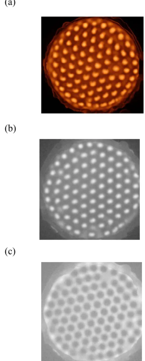
When increasing the voltage amplitude in the conditions above, a few filaments form when the breakdown voltage is reached. Above a given voltage, these filaments fill the whole discharge surface, and form an hexagonal structure as shown in Fig. 2a in the case of a voltage of 500 V amplitude. The picture of Fig. 2a has been taken with a standard camera.
(a)
(b)
(c)
FIGURE 2. Observation of a hexagonal pattern, (a) with a conventional camera; (b) and (c) are taken with the ICCD camera. The gate lengths are respectively 2 µs and 4 µs and the exposure time is
16ms (see ∆t1 and ∆t2 on Fig. 3).
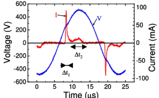
Figures 2b and 2c show the pictures obtained with the ICCD camera integrated over 2 and 4 µs respectively around the first current peak and the second current peak of the measured current represented on Fig. 3. Since the periodicity of the current is quite good (jitter much smaller than the current pulse duration), these images have been integrated over several cycles to get enough signal.
The time resolved pictures of Figs. 2b and 2c are very interesting because they show two different and embedded structures. The first one, which forms during the first current peak
(see Fig. 3) is an hexagonal pattern similar to the one that can be seen with the standard camera (Fig. 2a), but with a background light outside the filaments that seems relatively less important than in Fig. 2a.. The second structure forms during the second (and much smaller) current peak (see Fig. 3). It appears somehow as the negative of the pattern of Fig. 2b and exhibits a honeycomb structure where the centers of the cavities coincide with the maximum light intensity of the first structure.
0 5 10 15 20 25 -600 -400 -200 0 200 400 600 I V V o lt a g e ( V ) Time (µs) -100 -50 0 50 100 C u rr e n t (m A ) ∆t1 ∆t2 0 5 10 15 20 25 -600 -400 -200 0 200 400 600 I V V o lt a g e ( V ) Time (µs) -100 -50 0 50 100 C u rr e n t (m A ) ∆t1 ∆t2
FIGURE 3. Applied voltage and discharge current wave forms. Driving frequency 45 kHz,
inter-electrode gap 1 mm, DBD in Ne at 100Torr. ∆t1
and ∆t2 correspond the time intervals over which
the images of Figs. 2b and 2c respectively are integrated.
The results of Figs. 2 and 3 can be interpreted as follows. The first current peak corresponds to the formation of organized filaments in a transient glow regime. This current charges the dielectric surface until the voltage due to the surface charges induces a decreases of the gap voltage and a decay of the current. This is a well know feature of DBDs. However, since the applied voltage waveform continues to increase, the voltage across the gap will increase again after the current pulse. Since the charge deposited by the first current pulse on the dielectric surface is maximum in the centers of the filamentary discharges, i.e. the points of maximum light intensity of Fig. 2b, the voltage drop across the gap is larger away from these points and new discharges may be ignited first in the regions in between the filaments associated with the first pulse. The light (Fig. 2c) associated with the second current pulse of Fig. 3 is much more diffuse than the light of the filamentary discharges corresponding to the first pulse. This suggests that the regime of the discharge in the honeycomb structure of Fig. 2c is a Townsend discharge where a neutral plasma is actually
not present, and where the density of positive ions is much larger than the density of electrons. This explanation of the hexagonal and honeycomb structures of Fig. 2 is supported by the fluid models (next section below).
3.2. Results from a fluid model
The discharge model is based on solutions of ion and electron transport equations coupled with Poisson’s equation for the electric field in a 2D Cartesian geometry [4]. The charging of the dielectric layers is taken into account self-consistently. This 2D model has been previously used to describe the evolution of self-organized filaments in DBD[5] (see also the 3D model based on the same physical assumptionsand used in Ref. [6]).
Time (µs)
C
u
rr
en
t
(m
A
/c
m
)
V
o
lt
ag
e
(V
)
0 650V
I
0 1 250 270 230Time (µs)
C
u
rr
en
t
(m
A
/c
m
)
V
o
lt
ag
e
(V
)
0 650 0 650V
I
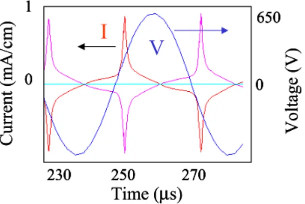
0 1 0 1 250 270 230 250 270 230FIGURE 4: Applied voltage and calculated (2D model) current waveforms. DBD in Ne, 50 torr, dielectric layer thicknesses 2 mm, gap length 2 mm, applied voltage amplitude 650 V, and frequency 25 kHz, secondary emission coefficient 0.1. The current on each electrode is shown.
Simulations have been performed for conditions similar but not identical to those of the experimental results above (so that comparisons are only qualitative): Ne at 50 torr, dielectric layer thickness 2 mm, gap length 2 mm, sinusoidal voltage waveform at 25 kHz, 600 V amplitude. The secondary electron emission coefficient is supposed to be equal to 0.1. The applied voltage and calculated current waveforms are plotted in Fig. 4. The current is similar to the measured current, the second pulse being less apparent than in the experiment.
P
o
si
ti
o
n
(
cm
)
(a)
P
o
si
ti
o
n
(
cm
)
(a)
P
o
si
ti
o
n
(
cm
)
0
1
0.5
(b)
P
o
si
ti
o
n
(
cm
)
0
1
0.5
0
1
0.5
(b)
Time (µs)
P
o
si
ti
o
n
(
cm
)
I
V
250
270
230
0
1
0.5
(c)
t
1t
2Time (µs)
P
o
si
ti
o
n
(
cm
)
I
V
250
270
230
0
1
0.5
(c)
Time (µs)
P
o
si
ti
o
n
(
cm
)
I
V
250
270
230
0
1
0.5
(c)
P
o
si
ti
o
n
(
cm
)
I
V
250
270
230
250
270
230
0
1
0.5
0
1
0.5
(c)
t
1t
1t
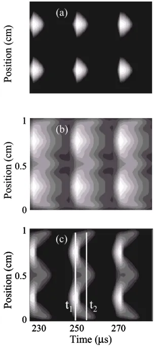
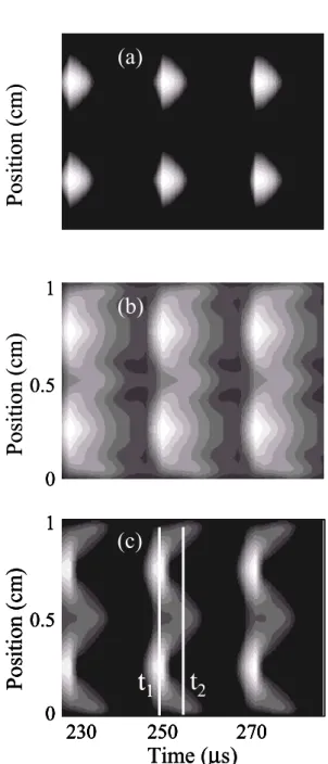
2FIGURE 5: Calculated (a) electron density, (b) ion density, and (c) ionization rate, in the conditions of Fig. 4, spatially integrated along the discharge axis and represented over three half-waves of the voltage as a function of transverse direction and time. Log scale, two decades. The maximum electron number densities are on the order of 0.5 1012 cm-3. Timing is the same as in Fig. 4. At time indicated t1 on Fig. 5c, the pattern corresponds
to the hexagonal pattern of Fig. 2b. At time t2
the pattern corresponds to the honeycomb structure of Fig. 2c.
The calculations are performed in a Cartesian simulation domain in the plane defined by the discharge axis (axial direction) and a direction parallel to the electrodes (transverse direction). The results can therefore not be presented in a
form directly comparable with Fig. 2. One interesting way to look at the results is to plot the discharge properties (e.g. electron density, ion density, ionization rate …) integrated along the discharge axis and as a function of transverse position and time. Such plots are represented in Fig. 5. We see on Fig. 5 that a periodic pattern is formed during the first current pulse, as in the experiment. The pattern that would be seen at time t1 of Fig. 5c
corresponds to the hexagonal pattern of Fig. 2b. After the first pulse, a second regime takes place where the electron density is much smaller than the ion density and the ionization rate is non zero only in regions outside the locations of the first periodic structure. The pattern that would be seen at time t2 of Fig. 5c
corresponds to the honeycomb structure of Fig. 2c. Obviously (because electron and ion densities are on the same order at time t1 in
Fig. 5, while the ion density is much larger than the electron density at time t2), time t1
corresponds to a filamentary glow discharge while time t2 corresponds to a Townsend
discharge.
This tends to suggest that the regime associated with the first pulse is a transient filamentary and self-organized glow discharge (similar to the hexagonal pattern of Fig. 2b), while the second pulse corresponds to a Townsend regime where a plasma is not formed and light is emitted in regions outside the filaments of the first current pulse (honeycomb structure of Fig. 2c).
4. CONCLUSION
DBDs give rise to a large variety of static and dynamic patterns. In this paper we have illustrated how detailed ICCD images of the discharge associated with fluid models can help understanding and clarifying the mechanisms responsible for pattern formation. We have shown an example of double pattern that can only be seen with a high speed camera and that is composed of an hexagonal structure superimposed on a honeycomb structure of the light emitted by the discharge. The two patterns occur successively in time and are associated respectively with a filamentary glow regime and with a diffuse Townsend discharge. Future work includes the experimental and numerical study of different
static and dynamical patterns in DBDs, and will be aimed at understanding the phase transitions between chaotic, organized, and homogeneous forms of these discharges.
REFERENCES
[1] U. Kogelschatz, IEEE Trans. Plasma Sci 30, 1400 (2002)
[2] I. Radu, R.Bartnikas, G.Czeremuszkin, and
M.R. Wertheimer IEEE Trans. Plasma Sci 31, 411 (2003)
[3] L. Dong, F. Liu, S. Liu, Y. He, and W. Fan Physical Review E 72 (2005)
[4] C. Punset, J.P Boeuf, and L.C. Pitchford, J Appl Eur. Phys. J. Appl. Phys. 83, 1884 (1998) [5] I. Brauer, C. Punset, H.-G. Purwins, J. P.
Boeuf, J. Appl. Phys. 85,7569 (1999)
[6] L. Stollenwerk, Sh. Amiranashvili, J.P. Bœuf, and H.-G. Purwins, Phys. Rev. Lett. 96, 255001 (2006)
FIGURE 3: Experimental setup
(a)
(b)
(c)
FIGURE 4. Observation of a hexagonal pattern, (a) with a conventional camera; (b) and (c) are taken with the
ICCD camera. The gate lengths are respectively 2 µs and 4 µs and the exposure time is 16ms (see ∆t1 and ∆t2 on
0 5 10 15 20 25 -600 -400 -200 0 200 400 600 I V V o lt a g e ( V ) Time (µs) -100 -50 0 50 100 C u rr e n t (m A ) ∆t1 ∆t2 0 5 10 15 20 25 -600 -400 -200 0 200 400 600 I V V o lt a g e ( V ) Time (µs) -100 -50 0 50 100 C u rr e n t (m A ) ∆t1 ∆t2
FIGURE 3. Applied voltage and discharge current wave forms. Driving frequency 45 kHz, interlectrode gap 1
mm, DBD in Ne at 100Torr. Dt1 and Dt2 correspond the time intervals over which the images of Figs. 2b and 2c
respectively are integrated.
Time (µs)
C
u
rr
en
t
(m
A
/c
m
)
V
o
lt
ag
e
(V
)
0 650V
I
0 1 250 270 230Time (µs)
C
u
rr
en
t
(m
A
/c
m
)
V
o
lt
ag
e
(V
)
0 650 0 650V
I
0 1 0 1 250 270 230 250 270 230FIGURE 4: Applied voltage and calculated (2D model) current waveforms. DBD in Ne, 50 torr, dielectric layer thicknesses 2 mm, gap length 2 mm, applied voltage amplitude 650 V, and frequency 25 kHz, secondary emission coefficient 0.1. The current on each electrode is shown.
P
o
si
ti
o
n
(
cm
)
(a)
P
o
si
ti
o
n
(
cm
)
(a)
P
o
si
ti
o
n
(
cm
)
0
1
0.5
(b)
P
o
si
ti
o
n
(
cm
)
0
1
0.5
0
1
0.5
(b)
Time (µs)
P
o
si
ti
o
n
(
cm
)
I
V
250
270
230
0
1
0.5
(c)
t
1t
2Time (µs)
P
o
si
ti
o
n
(
cm
)
I
V
250
270
230
0
1
0.5
(c)
Time (µs)
P
o
si
ti
o
n
(
cm
)
I
V
250
270
230
0
1
0.5
(c)
P
o
si
ti
o
n
(
cm
)
I
V
250
270
230
250
270
230
0
1
0.5
0
1
0.5
(c)
t
1t
1t
2FIGURE 5: Calculated (a) electron density, (b) ion density, and (c) ionization rate, in the conditions of Fig. 4, spatially integrated along the discharge axis and represented over three half-waves of the voltage as a function of transverse direction and time. Log scale, two decades. The maximum electron number densities are on the order
of 0.5 1012 cm-3. Timing is the same as in Fig. 4. At time indicated t1 on Fig. 5c, the pattern corresponds to the