UNIVERSITÉ DE MONTRÉAL
CONDUCTING POLYMERS AND NATURAL MOLECULAR MATERIALS FOR BIOELECTRONICS AND ENERGY STORAGE
PRAJWAL KUMAR
DÉPARTEMENT DE GÉNIE CHIMIQUE ÉCOLE POLYTECHNIQUE DE MONTRÉAL
THÈSE PRÉSENTÉE EN VUE DE L’OBTENTION DU DIPLÔME DE PHILOSOPHIAE DOCTOR
(GÉNIE CHIMIQUE) DÉCEMBRE 2016 © Prajwal Kumar 2016.
UNIVERSITÉ DE MONTRÉAL
ÉCOLE POLYTECHNIQUE DE MONTRÉAL
Cette thèse intitulée:
CONDUCTING POLYMERS AND NATURAL MOLECULAR MATERIALS FOR BIOELECTRONICS AND ENERGY STORAGE
présentée par : KUMAR Prajwal
en vue de l’obtention du diplôme de : Philosophiae Doctor a été dûment acceptée par le jury d’examen constitué de : M. BUSCHMANN Michael, Ph. D., président
M. CICOIRA Fabio, Ph. D., membre et directeur de recherche
Mme SANTATO Clara, Doctorat, membre et codirectrice de recherche M. KÉNA-COHEN Stéphane, Ph. D., membre
ACKNOWLEDGEMENTS
I am grateful for all the support and guidance I have received over the last 4 years at Polytechnique Montreal. First and foremost, I am immensely grateful to my advisor, Fabio Cicoira, for giving me the opportunity to work in his research group. Without your continuous support and encouragement, Fabio, it would have not been possible to reach this stage. It was truly a pleasure to work with you. I am very thankful to my co-supervisor Clara Santato, not only for her research advices but also for her moral support. Her patience and laboratory space were invaluable. My next acknowledgement goes to a visiting professor, specializes in the field of electrochemistry, Dr Francesca Soavi. I am indebted for her guidance, which helped me to improve the knowledge of electrochemistry. I am grateful to Dr. Alessandro Pezzella for the time spent together during his visit to our laboratory and demonstration of his vast experience of melanin synthesis. I gratefully acknowledge funding from Natural Sciences and Engineering Research Council of Canada (NSERC) and the Groupe de Recherche en Sciences et Technologies Biomédicales (GRSTB). My special gratitude goes to Daniel Pilon, Christophe Clément, Alireza H. Mesgar, Yves Drolet, Francis Boutet, Marie-Hélène Bernier, Robert Delisle and Josianne Lefebvre for their technical assistance during four years. Throughout all the time I spent at Polytechnique Montreal, my friends and colleagues helped me to build such a memorable and enjoyable experience. I have to mention many, especially Irina, Shiming, Gaia, Zhihui, Fanny, Guido, Xiang, Eduardo, Tian, Xu, Elizabeth, Hao, Jonathan, Julia, Dilek, Francis, Frédéric, Colleen, Tania, Samik, Laurie, Amel, Dominic, Arvindh, Sampath, Suchakra, Tanushree, Gabriel, Mengjiao, Xinhe, Xiaojie. It was pleasure to work with you. Also thanks to Polytechnique Montreal for academic and administrative services.
Finally, through all this I have had the unflagging support of my family: my mom and dad, Niriksha my sister and my brothers. Thank you for making me smiling, laughing and relaxed.
RÉSUMÉ
La découverte de la conduction électronique dans les matériaux organiques, dans les années 70, est à l’origine du développement des technologies optoélectroniques organiques. La remarquable propriété que présentent les semiconducteurs organiques de conduire les ions, en plus des porteurs de charge électroniques, a permis l’émergence d’un nouveau domaine de l’optoélectronique organique, c’est à dire la bioélectronique. La bioélectronique organique ouvre de nouvelles opportunités d’interface entre l’électronique organique et la biologie, avec la promesse d’applications dans des domaines aussi variés que les biocapteurs, la livraison de médicament, l’enregistrement et la stimulation neural. Combiner un transport ionique et électronique dans les semiconducteurs organiques utilisés pour les transistors représente une tentative intéressante pour parvenir à des dispositifs bioélectroniques efficaces. Ces dispositifs opèrent à faible polarisation de l’électrode de grille, grâce à la formation d’une double couche électrique au niveau de l’interface électrode/électrolyte. Les capacitances de double couches résultantes ont des valeurs qui dépassent de plusieurs ordres de grandeurs celles typiques des interfaces métal/diélectrique, en raison de la faible épaisseur (ca. 3nm) des doubles couches électriques. Par conséquent, les capacitances de double couche peuvent mener à de plus fortes modulations en courant pour des différences de potentiel de grille plus faibles (~1 V), compatibles avec les milieux aqueux.
Le cœur de cette thèse de doctorat est dévoué à une meilleure compréhension des mécanismes d’opération d’une classe importante de dispositifs bioélectroniques organiques, c’est-à-dire les transistors électrochimiques organiques (OECTs), dans le but d’optimiser leurs performances et de concevoir de nouveaux dispositifs bioélectroniques. Les OECTs sont formés d’un canal en polymère conducteur ainsi que d’une électrode de grille mis en contact avec le canal au travers d’un électrolyte. L’application d’une différence de potentiel électrique au niveau de la grille entraîne l’inclusion d’ions de l’électrolyte à l’intérieur de la couche mince en polymère en qui changent sa conducitvité initiale. Dans cette thèse, nous nous sommes concentrés sur le poly(3,4-éthylènedioxythiophène) dopé avec du poly(styrène sulfonate) (PEDOT:PSS) en tant que matériau actif dans le canal de OECTs.
Nous avons utilisé différentes épaisseurs de canal ainsi que deux électrolytes différents : le bromure de cétyltriméthyl-ammonium (CTAB), un surfactant apte à former des micelles, et du
NaCl. Les rapports ON/OFF les plus élevés ont été obtenus pour de transistors utilisant de faibles épaisseurs (~ 50 nm) de la couche mince et le CTAB comme électrolyte. La voltammétrie cyclique suggère qu’une réaction rédox entre les molécules d’oxygène dissoutes dans l’électrolyte et le PEDOT:PSS mène à de faibles ratios ON/OFF quand le NaCl est utilisé comme électrolyte. La voltammétrie cyclique et la spectroscopie d’impédance électrochimique révèlent que le dopage/dédopage du canal devient plus lent à des épaisseurs relativement élevés de la couche mince et en présence d’ions de plus grande taille.
Les caractéristiques de l’électrode de grille ont des effets significatifs sur le comportement des OECTs. Dans cette thèse, du carbone activé (AC) avec une importante surface spécifique a été utilisé comme matériau pour l’électrode de grille dans les OECTs basés sur le PEDOT:PSS. L’utilisation d’électrodes de grille en AC de grande surface, a mené à une importante modulation en courant drain-source dans les OECTs et à la limitation des réactions électrochimiques indésirables.
La biocompatibilité et la biodégradabilité des matériaux utilisés en bioélectronique organique sont essentiels. Ces propriétés sont importantes même pour des dispositifs alimentant les dispositifs bioélectroniques. La mélanine est un biopigment abondant en nature et doté d’activité redox. Ce biopigment peut être mis en forme à température ambiante et est donc un matériau extrêmement intéressant pour le développement de dispositifs de stockage de l’énergie biocompatibles et « verts ». L’eumélanine est une des formes de la mélanine qui est particulièrement étudiée par les chercheurs en science de matériaux. Celle-ci se retrouve dans de nombreuses parties du corps humain, dont la peau, les cheveux, l’oreille interne et le cerveau. L’eumélanine réalise de nombreuses fonctions dans le corps humain comme l’absorption dans une large bande du spectre UV-visible ou encore la chélation métallique. Dans cette thèse, nous rapportons les propriétés de stockage d’énergie électrochimique de la part d’électrodes basées sur l’eumélanine, en configuration supercondensateur. L’eumélanine est formée de monomères faits de 5,6-dihydroxyindole (DHI) et d’acide 5,6-dihydroxyindole carboxylique (DHICA), présents sous différentes formes redox (hydroxyquinone, semiquinone et quinone). La synergie entre l’activité redox des monomères et la capacité de plusieurs de leurs fonctionnalités à lier des cations de façon réversible permet l’utilisation de l’eumélanine dans des dispositifs de stockage
d’énergie fonctionnant en mode pseudocapacitif. En partant de la démonstration des supercondensateurs basés sur l’eumélanine, nous avons utilisé une approche non-conventionnelle pour fabriquer des micro-condensateurs flexibles sur substrats plastiques.
ABSTRACT
The discovery of electronic conduction in carbon-based materials, in the 1970s, is the basis of the development of organic optoelectronics technologies. The remarkable property of organic semiconductors to conduct ions, in addition to electronic charge carriers, has recently offered a new emerging direction in organic optoelectronics, called organic bioelectronics. Organic bioelectronics opens the opportunity to interface organic electronics with biology with promising applications such as biosensing, drug delivery, neural recording and stimulation. Combining ionic and electronic transport in organic semiconductors into transistor architectures represents an interesting attempt to achieve efficient bioelectronics devices. These devices operate at low gate biases, due to the formation of electrical double layers at electrode/electrolyte interfaces. The resultant double layer capacitances are a few orders of magnitude higher compared to capacitances typical of metal/dielectric interfaces, due to the low thickness (ca. 3 nm) of the electrical double layers, which consequently leads to higher current modulations at lower gate voltage (~1 V).
The core of this Ph.D. thesis is devoted to a better understanding of the operational mechanism of an important class of organic bioelectronics devices, i.e. organic electrochemical transistors (OECTs), to optimize their performance and to design novel bioelectronics devices. OECTs consist of a conducting polymer channel and a gate electrode in contact with an electrolyte. The application of a gate electrical bias triggers the inclusion of electrolyte ions into the polymer film thus changing its initial conductivity. In this thesis we focus on poly(3,4-ethylenedioxythiophene) doped with polystyrenesulfonate (PEDOT:PSS) as the active material in OECTs.
We employed various channel thicknesses and two different electrolytes: the micelle-forming surfactant cetyltrimethyl ammonium bromide (CTAB) and NaCl. The highest transistor ON/OFF ratios were achieved at low film thicknesses (~ 50 nm), using CTAB as the electrolyte. Cyclic voltammetry suggested that a redox reaction between molecular oxygen dissolved in the electrolytes and PEDOT:PSS leads to low ON/OFF ratios when NaCl was used as the electrolyte. Cyclic voltammetry and electrochemical impedance spectroscopy revealed that doping/dedoping of the channel becomes slower at relatively high film thickness and in the presence of bulky ions. The characteristics of the gate electrode have significant effects on the behavior of OECTs. In this thesis, high specific surface area activated carbon (AC) was used as gate electrode material in
OECTs based PEDOT:PSS. The use of high surface area carbon gate electrodes led to the high drain-source current modulation in OECT and limited undesirable electrochemical processes.
The biocompatibility and biodegradability property of the materials used in organic bioelectronics is of course of primary importance. These features are important even for devices powering the bioelectronics devices. Melanin is a redox active biopigment abundant in nature. The biopigment can be processed at room temperature and, as such, it is an extremely attractive material for environmentally and human friendly energy storage solutions. A form of melanin highly investigated by materials scientists is eumelanin, found in many parts of the human body including skin, hair, inner ear and brain. Eumelanin has many functions in the human body, such as strong broad-band UV-visible absorption and metal chelation. In this thesis, we report the ion storage property of eumelanin-based electrodes assembled in supercapacitors. Eumelanin is based on 5,6-dihydroxyindole (DHI) and 5,6-dihydroxyindole carboxylic acid (DHICA) building blocks, present in different redox forms (hydroxyquinone, semiquinone and quinone). The synergy between the redox activity of the building blocks and the capability of several of their functionalities to reversibly bind cations constitutes the foundation for the use of melanin in pseudocapacitive energy storage systems. Capitalizing on the demonstration of eumelanin-based supercapacitors, we used an unconventional patterning approach to fabricate binder-free flexible micro-supercapacitors on plastic substrates.
TABLE OF CONTENTS
ACKNOWLEDGEMENTS ... III RÉSUMÉ ... IV ABSTRACT ... VII TABLE OF CONTENTS ... IX LIST OF TABLES ... XII LIST OF FIGURES ... XIII LIST OF SYMBOLS ... XIX LIST OF ABBREVIATIONS ... XXI LIST OF APPENDICES ... XXII
CHAPTER 1 INTRODUCTION ... 1
1.1 OVERVIEW ... 1
1.2 Π - CONJUGATED SYSTEMS ... 2
1.3 ORGANIC ELECTRONIC MATERIALS ... 3
1.4 ORGANIC ELECTRONICS DEVICES ... 7
1.4.1 Organic light-emitting diodes (OLEDs) ... 7
1.4.2 Organic photovoltaics ... 8
1.4.3 Organic thin film transistors ... 9
1.5 ORGANIC BIOELECTRONIC DEVICES ... 14
1.6 SUPERCAPACITORS ... 15
1.7 PROBLEM IDENTIFICATION ... 18
1.8 GENERAL OBJECTIVES ... 18
1.8.1 Motivation ... 19
1.8.2 Specific objectives ... 19
1.9 ORGANIZATION OF THE WORK ... 20
CHAPTER 2 BIOELECTRONIC MATERIALS, DEVICES AND LITERATURE REVIEW .. 23
2.1 PEDOT ... 23
2.1.2 Conductivity Enhancement of PEDOT :PSS ... 26
2.2 ORGANIC ELECTROCHEMICAL TRANSISTORS (OECTS) ... 27
2.2.1 Working Principle of PEDOT:PSS based OECT ... 28
2.3 MELANIN ... 31
2.3.1 Melanin Electrochemistry ... 33
CHAPTER 3 ARTICLE 1: EFFECT OF CHANNEL THICKNESS, ELECTROLYTE IONS AND DISSOLVED OXYGEN ON THE PERFORMANCE OF ORGANIC ELECTROCHEMICAL TRANSISTORS ... 36
3.1 AUTHORS ... 36
3.2 ABSTRACT ... 36
3.3 INTRODUCTION ... 37
3.4 EXPERIMENTAL ... 38
3.5 RESULTS AND DISCUSSIONS ... 38
3.6 CONCLUSION ... 47
3.7 ACKNOWLEDGMENTS ... 47
CHAPTER 4 ARTICLE 2: MELANIN-BASED FLEXIBLE SUPERCAPACITORS ... 48
4.1 AUTHORS ... 48
4.2 ABSTRACT ... 49
4.3 INTRODUCTION ... 49
4.4 RESULTS AND DISCUSSIONS ... 52
4.4.1 Cyclic Voltammetry Studies on Melanin ... 52
4.4.2 Melanin-based Supercapacitor ... 54
4.4.3 Melanin-based Micro-supercapacitors ... 59
4.5 CONCLUSIONS ... 63
4.6 EXPERIMENTAL SECTION ... 64
4.6.1 Materials ... 64
4.6.2 Fabrication of Melanin Electrodes on Carbon Paper (Mel/CP Electrodes) ... 64
4.6.3 Structures of the Supercapacitors and Micro-supercapacitors ... 65
4.6.4 Unconventional Lithography Steps for Micro-supercapacitors on Plastics ... 65
4.6.5 Electrochemical Set-up ... 66
4.6.7 Scanning Electron Microscopy (SEM) ... 66
4.7 ACKNOWLEDGMENTS ... 66
CHAPTER 5 ACTIVATED CARBON GATE ELECTRODES FOR ORGANIC ELECTROCHEMICAL TRANSISTORS (OECT) ... 68
5.1 FABRICATION OF ORGANIC ELECTROCHEMICAL TRANSISTORS ... 69
5.2 PREPARATION OF PEDOT:PSS PROCESSING MIXTURE ... 69
5.3 PREPARATION OF THE ACTIVATED CARBON ELECTRODES ... 70
5.4 ORGANIC ELECTROCHEMICAL TRANSISTOR CHARACTERIZATION ... 70
CHAPTER 6 EUMELANIN ELECTROCHEMISTRY: ;COMPLEMENTARY RESULTS ... 73
6.1 ELECTROCHEMICAL SET-UP ... 74
6.2 IRREVERSIBLE OXIDATION PEAK ... 74
6.3 MELANIN ON CARBON PAPER ELECTRODES ... 75
6.3.1 Fabrication of melanin electrodes on carbon paper (Mel/CP electrodes) ... 76
6.3.2 The influence of aqueous electrolytes on the performance of Mel/CP electrodes ... 78
6.4 SIGMA MELANIN COMPARISON WITH DMSO MELANINS ... 79
CHAPTER 7 GENERAL DISCUSSION ... 83
CHAPTER 8 CONCLUSION AND PERSPECTIVES ... 85
BIBLIOGRAPHY ... 88
LIST OF TABLES
Table 3.1 ON/OFF ratios extracted from transfer characteristics (-0.4 V ≤ Vgs ≤ 0.6 V and Vds
=-0.2 V) of PEDOT:PSS OECTs with four different channel thickness (~500, 180, 110, 50 nm) using 0.01 M NaCl and 0.001 M CTAB as the electrolytes. ... 41 Table 3.2. Capacitance and amount of dedoping/doping charge (absolute and volumetric values) of PEDOT:PSS films extracted from the anodic voltammetric currents at 5 mV/s in NaCl and CTAB electrolytes. The film volumes are 3.0×10⁻⁵ cm3 for the thick film and 3.4×10⁻⁶ cm3 for the thin film. ... 43
LIST OF FIGURES
Figure 1.1 Chemical structure of a) polyethylene and b) polyacetylene. ... 3 Figure 1.2 Schematic representation of sp2 hybridized orbitals of ethylene molecule. The sp2
hybrid orbitals are shown in light gray color, and the non hybridized pz orbitals in light
violet. The pz orbitals extend in and out of the plane of the molecule. ... 3
Figure 1.3 Molecular structure of two relevant conjugated polymers in organic electronics.[9] Reprinted with permission. Copyright © 2010, Royal Society of Chemistry. ... 4 Figure 1.4 Molecular structure of relevant conjugated small-molecule organic semiconductors. (a) Pentacene. (b) Sexithiophene (6T). (c) Dihexylsexithiophene (DH6T, Hex-6T-Hex). (d) Copper phthalocyanine.[9] Reprinted with permission. Copyright © 2010, Royal Society of Chemistry. ... 4 Figure 1.5 The molecular structure of a few technologically relevant conjugated polymers and their electronic band gap.[17] ... 6 Figure 1.6 Structure of one of the first reported single-layer organic light-emitting diode.[5] Reprinted with permission. Copyright © 1999, Rights Managed by Nature Publishing Group. ... 7 Figure 1.7 Schematic illustration of an OPV cell (a) I–V characteristics of a PV cell under dark (blue) and illumination (red) conditions (b) Schematic illustration of photocurrent generation processes for the OPV cells (c) [25] Reprinted with permission. Copyright © 2013 by Sou Ryuzaki and Jun Onoe. ... 9 Figure 1.8 Schematic representation of an organic transistor. ... 10 Figure 1.9 Charge carrier mobility of p-channel and n-channel transistors based on
small-molecule and polymeric semiconductors. [9] Reprinted with permission. Copyright © 2010, Royal Society of Chemistry. ... 11 Figure 1.10 Schematic representation of EG transistors and their subcategories, depending on the working mechanism (on the left the mechanism of doping is electrostatic, on the right it is electrochemical). ... 13
Figure 1.11 Organic bioelectronics: biological moieties, including cells, micro-organisms, proteins, oligonucleotides, and small molecules, can be interfaced with organic electronics devices to yield biosensors, medical diagnostics, tools for biomedical research, and bioelectronic implants that will have a major impact in health care [41]. Reprinted with permission. Copyright © Materials Research Society 2010. ... 14 Figure 1.12 (a) Equivalent circuit model for an electrochemical capacitor; b) Schematic representation of a two-electrode supercapacitor; (c) Schematic illustrations of the typical structure of a conventional supercapacitor (d) and its flexible counterpart.[53] Reprinted with permission. Copyright © 2014, Royal Society of Chemistry. ... 16 Figure 2.1 Molecular structure of poly(3,4-ethylenedioxythiophene) (PEDOT). ... 23 Figure 2.2 Schematic representation of various applications of PEDOT.[67] ... 24 Figure 2.3 Molecular structure of PEDOT:PSS. A hole is indicated on the PEDOT chain in red, in the form of a positive polaron. The acceptor on the PSS chain is indicated in blue.[68] Reprinted with permission. Copyright © 2013, Rights Managed by Nature Publishing group. ... 25 Figure 2.4 Chemical polymerization of ethylenedioxythiophene in the presence of polystyrenesulfonic acid.[61] ... 26 Figure 2.5 (a) Device structure and electrical circuit of a PEDOT:PSS OECT; (b and c) OECT working principle; circles filled with - indicate PSS− ions and + indicate mobile holes.[91] Reprinted with permission. Rights managed by AIP Publishing LLC. ... 28 Figure 2.6 Potential distribution between the gate electrode and the channel for two device geometries (a) The transistor with the small gate (Ach/Ag = 100) (b) The transistor with the
bigger gate (Ach/Ag = 0.01).[85] Reprinted with permission. Copyright © 2010 Wiley
Periodicals, Inc. ... 30 Figure 2.7 Potential distribution between the gate electrode and the channel for Ag and Pt gate electrodes.[91] Reprinted with permission. Rights managed by AIP Publishing LLC. ... 30 Figure 2.8 Molecular structures of eumelanin precursors: a) dopamine, b)
3,4-dihydroxy-L-phenylalanine (DOPA), c) 5,6-dihydroxyindole (DHI) and d) 5,6-dihydroxyindole carboxylic acid (DHICA). ... 32
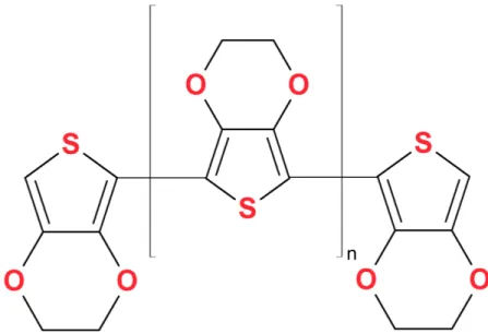
Figure 2.9 Various redox forms of eumelanin building blocks DHI and DHICA. ... 33 Figure 2.10 Raman spectra of eumelanins. (A) natural melanin and Na-loaded natural melanin; (B) synthetic melanin and Na-loaded synthetic melanin; (C) electrodeposited melanin and Na-loaded electrodeposited melanin. Raw spectra (black lines) are deconvoluted into five bands using a Voigt function.[118] Copyright © (2013) National Academy of Sciences. .... 34 Figure 2.11 The mechanism of Mg2+ binding melanin catechols.[119] Reprinted with permission. Copyright © 2014 WILEY-VCH Verlag GmbH & Co. KGaA, Weinheim. ... 34 Figure 3.1 Sheet resistance (red circles, left y axis) and electrical conductivity (blue stars, right y axis) of PEDOT:PSS films (geometric area 15x15 mm2) of different thicknesses (~500, 180, 110, and 50 nm). The error bars correspond the standard deviation of four samples. ... 39 Figure 3.2 Transfer characteristics (-0.4 V ≤ Vgs ≤ 0.6 V and Vds = -0.2 V) of PEDOT:PSS
OECTs with four different channel thicknesses (~500, 180, 110, 50 nm) using 0.01 M NaCl (a) and 0.001 M CTAB (b) as the electrolyte. OECT based on a 110 nm thick PEDOT:PSS film using 0.001 M CTAB as the electrolyte, showing a high ON/OFF ratio of ~1700 (-0.8 V≤Vgs≤0.5 V and Vds=-0.5 V). The blue star represents the ON and OFF currents at Vgs
=-0.8 and Vgs=0.6 V (c). Hysteresis behavior of an OECT based on a 50 nm thick PEDOT:PSS
film(d). The black curve corresponds to the forward bias (from Vgs=-0.4 to Vgs=0.6 with
Vds=-0.2 V) and the red curve to the reverse bias. During all OECTs characteristics, gate
scan rate of 0.003 V/s was maintained. ... 40 Figure 3.3 Cyclic voltammetry of PEDOT:PSS films (∼250 nm thickness) using 0.01M NaCl and 0.001M CTAB as the electrolytes, carried out under N2 purging (a). Cyclic voltammetry of
PEDOT:PSS films (50 nm and ∼500 nm thicknesses) using 0.01M NaCl as the electrolyte, carried out under N2 purging (b). Cyclic voltammetry of PEDOT:PSS films (∼50 nm
thickness) carried out under N2 or air purging using 0.01M NaCl (c) and 0.001M CTAB (d)
as the electrolyte. ... 42 Figure 3.4 Electrochemical impedance spectroscopic analysis (Nyquist plots) of PEDOT:PSS films (thicknesses ~500 nm and ~50 nm) in 0.01 M NaCl (a) and 0.001 M CTAB (b) electrolytes. PEDOT:PSS is used as working electrodes, a Pt foil as counter electrode, and Ag/AgCl as reference. The frequency range is 0.5 kHz to 10-4 kHz with an AC amplitude of
5 mV. The PEDOT:PSS films were doped at 0.6 V vs Ag/AgCl for 30 s prior to EIS by chronoamperometry. ... 46 Figure 4.1 (a) Cyclic voltammetry of 33.8 µg/cm2 and 67.5 µg/cm2 Mel/CP electrodes and bare carbon paper (CP, control sample) in NH4CH3COO(aq) pH 5.5; scan rate 50 mV/s. (b) SEM
image, acquired in BSE mode, of a sample made of melanin on carbon paper (CP, loading of ca 0.9 mg/cm2) stained with uranyl acetate. The bright areas correspond to melanin chelating the uranyl oxycation. Acceleration voltage 10 kV. (c) Cyclic voltammetry of 33.8 µg/cm2 Mel/CP in NH4CH3COO(aq) pH 5.5 at different scan rates. (d) Specific capacitance and
capacity vs. scan rate of Mel/CP electrodes (33.8 µg/cm2), in NH4CH3COO(aq) at pH 5.5.
Geometric size of the samples 0.4 cm2. ... 54 Figure 4.2 Mel/CP supercapacitors with two identical Mel/CP electrodes of equal loadings and with NH4CH3COO(aq) pH 5.5 electrolyte. (a) Cell voltage and electrode potential profiles
during a charge–discharge galvanostatic cycle (20th cycle) obtained at 12.5 mA/cm2 with 67.5 µg/cm2 Mel/CP (each electrode). (b) Capacitance density vs. current density, for three
different melanin loadings. (c) Ragone plots extracted from galvanostatic discharge cycles for different melanin loadings with current density of 0.125, 0.25, 1.25, 2.5, 5, 12.5, 17.5, 25, 37.5 mA/cm2. ... 56 Figure 4.3 Working principle of melanin-based supercapacitors constituted by two identical negative and positive electrodes, immersed in NH4CH3COO-(aq) pH 5.5. a) Situation before a
potential is applied between the electrodes, b) situation produced during charging and c) situation produced during the discharging of the electrodes. See Scheme 1 for the chemical structure of H2Q, SQ and Q groups. ... 58
Figure 4.4 Process flow for fabrication of micro-supercapacitors on flexible PET substrates: (a) a glass slide is covered with PDMS; (b) PET is laminated on the glass slide; (c) Parylene C is deposited by chemical vapor deposition; (d) Parylene C is patterned by photolithography and oxygen RIE to generate Parylene C-free regions on PET; (e) Ti (4 nm) and Au (40 nm) are deposited by e-beam evaporation; (f); melanin/carbon black slurry is drop cast; (g) Parylene C is peeled-off; (h) and (i) PET is removed from the glass slide to achieve the final flexible device. ... 60
Figure 4.5 Melanin-based flexible micro-supercapacitors with ~200 µg/cm2 melanin loading on
each electrode using NH4CH3COO(aq) pH 5.5 as the electrolyte. (a) Optical image of the
micro-supercapacitor (total three micro-supercapacitors) on a flexible PET substrate. (b) Areal capacitance and volumetric capacitance vs. scan rate of the cyclic voltammetry (obtained from Figures S10a and S10b) taking into account that the total area of the two electrodes is 0.16 cm2 and that the corresponding volume is about 2×10⁻⁴ cm3 (see Experimental) (c) Galvanostatic charge/discharge cycles with three different values of the current density (0.625, 1.25, and 12.5 mA/cm2). (d) Ragone plot extracted from the galvanostatic discharge cycles at different values of the current density (0.625, 1.25, 6.25, 12.5 and 25 mA/cm2). The area of each electrode is 0.08 cm2. ... 62 Figure 5.1 Scheme of the architecture of OECT using a conducting polymer channel made of PEDOT:PSS with a) AC gate electrode and b) PEDOT:PSS gate.[93] Reprinted with permission. Copyright © 2014 American Chemical Society. ... 68 Figure 5.2 Characteristics of PEDOT:PSS based OECT using AC and PEDOT:PSS gate electrodes, employing an aqueous solution of NaCl (0.01M) as the electrolyte. Typical output characteristics obtained with an AC (A) or a PEDOT:PSS gate electrode (B). The Vds
scan rate is 5 mV/s and Vgs is varied from −0.4 to +0.6 V in steps of 0.2 V. Transfer
characteristics (C) of PEDOT:PSS OECTs using an AC (black line) and a PEDOT:PSS gate electrode (red line) at Vds= −0.5 V and −0.6 V ≤ Vgs ≤ 0.8 V. Transient (Ids vs time)
responses (D) normalized with respect to the current at Vgs= 0 V of OECTs using AC (black
solid line) and PEDOT:PSS (red dashed line) gate electrodes at Vds= −0.5 V. From left to
right, Vgs is pulsed from 0 to −0.6, −0.4, −0.2, +0.2, +0.4, +0.6 and +0.8 V with pulse
duration of 100 s.[93] Reprinted with permission. Copyright © 2014 American Chemical Society. ... 70 Figure 5.3 (A) Steady state gate-source current (Igs) of OECTs with PEDOT:PSS (black line) and
AC of different geometric areas as gate electrodes. (B) Comparison of transfer current modulations for devices using AC gate electrodes of different geometric areas and a PEDOT:PSS gate electrode. An aqueous solution of NaCl (0.01 M) is used as the electrolyte.[211] Reprinted with permission. Copyright © 2014 American Chemical Society. ... 72
Figure 6.1 Cyclic voltammetry of (a) Sigma melanin, (b) DHI melanin, (c) DHICA melanin on ITO substrates as working electrode, platinum foil and saturated calomel electrode as the counter and the reference electrodes, respectively. Nitrogen purged PBS buffer (0.01 M) of pH 7.4 is used as the electrolyte and a 50 mV s-1 scan rate is maintained. The cyclic voltammogram of ITO without melanin in PBS is represented in gray. Black arrows indicate the decrease in current density as a function of the number of cycles.[113] ... 75 Figure 6.2 Cyclic voltammograms (first three cycles) of a Mel/CP electrode (33.8 µg/cm2
melanin loading, normalized over the electrode footprint) in NH4CH3COO(aq) at pH 5.5, at
50 mV/s. A broad anodic peak, with irreversible characteristics, is observed during the first cycle of the cyclic voltammetry of Mel/CP. Pt foil used as counter electrode. ... 76 Figure 6.3 Anodic current at 0 V (versus Ag/AgCl) versus scan rate, obtained from the cyclic voltammograms of Mel/CP with 33.8 µg/cm2 melanin loading in NH4CH3COO(aq) pH 5.5. 77
Figure 6.4 Cycling stability of 33.8 µg/cm2 Mel/CP in NH4CH3COO(aq) pH 5.5 at 50 mV/s. (a)
1,000 voltammetric cycles and (b) cyclic voltammograms extracted from (a) every 100 cycles. ... 77 Figure 6.5 Cyclic voltammograms at different scan rates of Mel/CP electrodes (33.8 µg/cm2
loading of melanin) in (a) sodium sulfate at pH 5.5, (b) phosphate buffered saline at pH 7.4 and (c) ammonia buffer at pH 10 (see Experimental in main text). Geometric size of samples 0.4 cm2. (d) Cyclic voltammograms of Mel/CP electrodes (33.8 µg/cm2 loading of melanin) at 100 mV/s. ... 79 Figure 6.6 Building blocks of DMSO melanins.[212] ... 80 Figure 6.7 Cyclic voltammograms (total 10 cycles) of (a) Sigma melanin (b) DMSO melanin RT and (c) DMSO melanin 100 °C and (d) capacitance values evaluated from the CV. 120 µg/ cm2 of melanin on carbon paper is the loading in the working electrode. NH4CH3COO(aq) 7.5
M (pH 5.5) was used an electrolyte, carbon paper strips were used also as counter electrode; scan rate 50 mV/s; the geometric area of the working electrode was 0.25 cm2. ... 81 Figure 7.1 (a) The repeating unit of eumelanin, a natural conjugated polymer pigment. (b) Synthetic PEDOT polymer. Similarities between melanin and PEDOT highlighted in red and green colors.[213] ... 84
LIST OF SYMBOLS
AC Activated carbons
ADH Alcohol dehydrogenase
Al Aluminum
Ag Silver
AgCl Silver chloride
Ar Argon
Au Gold
CE Counter electrode
CMC Critical micellar concentration
CTAB cetyltrimethylammonium bromide
D Drain
DBSA Dodecyl benzene sulfonic acid
EG Electrolyte-gated
EG-OFET Electrolyte gated field effect transistors EIS Electrochemical Impedance Spectroscopy FET Field-effect transistor
GOx Glucose oxidase
H2O2 Hydrogen peroxide
IL Ionic liquid
KCl Potassium chloride
NaCl Sodium chloride
OECTs Organic electrochemical transistors OFETs Organic field-effect transistors
OLEDs Organic light-emitting diodes
OTFTs Organic thin-film transistors
P3HT Poly(3-hexylthiophene)
PBS Phosphate-buffered saline
PEDOT:PSS Poly(3,4-ethylenedioxythiophene):polystyrenesulfonate
PET Polyethylene terephthalate
PLGA Poly(L-lactide-co-glycolide)
PSS Polystyrenesulfonate
Pt Platinum
RE Reference electrode
RIE Reactive ion etching
S Source
LIST OF ABBREVIATIONS
Ach Channel area
Ag Gate area
cch Channel capacitance per unit area
cg Gate capacitance per unit area
C Capacitance
D Thickness or distance between electrodes
e- Electron
E Stored energy
G Conductance of the channel
I Drain-source current at Vg≠0 V
I0 Drain-source current at Vg=0 V
Ids Source-drain current
Ion ON-state current
Ioff OFF-state current
Igs Gate-source current l Drift length L Length M+ Cations P Power t Time u Drift velocity
Vcell Cell voltage
Vds Drain-source voltage
Vgs Gate-source voltage
Vsol Solution voltage
LIST OF APPENDICES
Appendix A –SUPPORTING INFORMATION FOR ARTICLE MELANIN-BASED FLEXIBLE SUPERCAPACITORS ... 107 Appendix B – LIST OF PUBLICATIONS IN POLYTECHNIQUE MONTREAL NOT INCLUDED IN THE THESIS ... 130 Appendix C – PARTICIPATION IN THE CONFERENCES ... 132
CHAPTER 1 INTRODUCTION
This chapter constitutes an overview of organic electronics (OE) materials and devices, with particular attention given to organic bioelectronics and supercapacitors based on organic polymers. The chapter includes the identification of the scientific problems studied in the thesis as well as its general and specific objectives and motivation.
1.1 Overview
The history of organic electronics begins with the discovery of conducting polymers in 1976, by Heeger, MacDiarmid, and Shirakawa, who were awarded the Nobel Prize in Chemistry in 2000.[1] The discovery that π-conjugated organic molecules and polymers can be electrically conductive generate a great deal of enthusiasm in the scientific community and led to the rise of organic electronics.[2,3]
Organic semiconductors have captured the interest of the research community because of their unique properties, such as electro- and photoluminescence, ease of processing by several techniques (e.g. evaporation, spin coating, printing) and compatibility with a variety of substrates, including mechanically flexible ones. In 1987, Tang et al. demonstrated Tris-(8-hydroxyquinoline) aluminum (Alq3) based organic electroluminescent diodes.[4] In 1989, R.
Friend’s group demonstrated the successful use of poly(p-phenylene vinylene) (PPV) for efficient electroluminescent devices.[5] The first organic transistor was fabricated with polythiophene semiconducting thin films.[6] Since then, tremendous developments have taken place in organic electronics for a variety of applications, such as organic light-emitting diodes (OLED), organic field-effect transistors (OFET), and organic photovoltaics (OPV).[4,5,7-13] Some organic electronics products have been on the market for more than a decade. In 1997, Pioneer Corporation released the first commercial OLED product, a passive matrix OLED (PMOLED) display for car audio displays. A decade later, in 2007, Samsung Mobile Display released the first commercial active matrix OLED (AMOLED) display. Although various prototypes of white OLEDs for lighting have been demonstrated over the years, it was not until 2010 that OSRAM Opto Semiconductor released the first commercial white OLED lighting panel. Heliatek has been
commercializing OPV since 2006. Organic transistors find application in backplanes for flexible displays currently developed by Plastic Logic.[14]
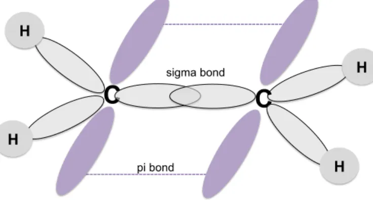
1.2 π - conjugated systems
The polymer polyethylene, where each carbon is bonded to two carbons and to two hydrogen atoms through four sigma (σ) bonds, is an insulator (Figure 1.1). On the other hand, polyacetylene, which contains alternating single (σ) and double (σ and π) carbon-carbon bonds, shows a certain electrical conductivity. This sequence of alternating σ and π bonds is called conjugation. Each carbon atom in the backbone of a conjugated polymer is sp2 hybridized. When polymerization of acetylene occurs, the singly occupied 2s orbital and two of the three singly occupied 2p orbitals (2px and 2py) of the carbon atom combine and form three sp2 hybrid orbitals
with equal energy. (Figure 1.2) These three hybridized orbitals are capable to form σ bonds to three neighboring atoms. The electrons involved in these bonds are strongly localized. The remaining 2pz orbital is located perpendicularly to the plan of the three sp2 hybrid orbitals. When
the 2pz orbitals of two adjacent carbon atoms overlap sideways, they combine leading to two
molecular orbitals: one π (bonding) and one π* (anti-bonding) orbital. The π bonding molecular orbital is lower energy than the atomic orbitals and anti-bonding π* molecular orbital is higher energy than the atomic orbitals. The energy difference between the highest occupied molecular orbital (HOMO) of π-orbital and the lowest unoccupied molecular orbital (LUMO) of π* orbital is known as energy gap or band gap. In a conjugated polymer containing n sp2 hybridized carbon atoms, there are a total of n 2pz atomic orbitals that combine to create n molecular orbitals. The π
electrons are delocalized along the entire backbone and the polymer can be seen as a one-dimensional metal. This means that the electrons in the π-bonds can be found between any of the carbon atoms and can thus move along the polymer chain. The delocalization of the π-electrons along the carbon backbone is the key to enable facile charge carrier transport within the polymer chain, thus making the polymer conductive.
Figure 1.1 Chemical structure of a) polyethylene and b) polyacetylene.
Figure 1.2 Schematic representation of sp2 hybridized orbitals of ethylene molecule. The sp2
hybrid orbitals are shown in light gray color, and the non hybridized pz orbitals in light violet.
The pz orbitals extend in and out of the plane of the molecule.
A low concentration of mobile charge carriers characterizes conjugated organic polymers in their intrinsic state. However, the electrical behavior of these materials can go from insulating to semiconducting and conducting. Highly-conducting polymers can be achieved by chemical doping, e.g. by chemical oxidation or reduction. For example, when polyacetylene is oxidized by AsF5, the conductivity increases from 10-5 S/cm to 200 S cm-1.[1,5,16]
1.3 Organic electronic materials
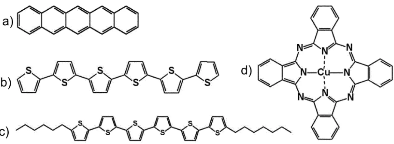
Organic semiconductors can be of two types: conjugated polymers and conjugated small-molecules. On the other hand, conjugated polymers showing metallic conductivity are known as conducting polymers. Several semiconducting and conducting polymers, such as polythiophenes (Figure 1.3a), have excellent solubility in a variety of organic solvents, therefore thin films can be readily prepared by spin coating, dip-coating, drop-casting, screen printing, or inkjet printing. Small-molecule organic semiconductors can be soluble or insoluble in common organic solvents.
a) b) --- ---
C
HC
H H pi bond sigma bond HInsoluble small-molecule organic semiconductors are often deposited by thermal evaporation. The most common examples of organic small-molecule semiconductors deposited by thermal evaporation are pentacene, sexithiophene and phthalocyanines (Figure 1.4). In most cases, thin films of small-molecule organic semiconductors have a polycrystalline structure and are characterized by polymorphism.
Figure 1.3 Molecular structure of two relevant conjugated polymers in organic electronics.[9] Reprinted with permission. Copyright © 2010, Royal Society of Chemistry.
Figure 1.4 Molecular structure of relevant conjugated small-molecule organic semiconductors. (a) Pentacene. (b) Sexithiophene (6T). (c) Dihexylsexithiophene (DH6T, Hex-6T-Hex). (d) Copper phthalocyanine.[9] Reprinted with permission. Copyright © 2010, Royal Society of Chemistry. S n polythiophene n S CH3 poly(3-hexylthiophene)
a)
b)
c)
d)
The bandgap of organic semiconductors can be tailored by controlling the conjugation length. The longer the extension of the conjugation in the molecule, the smaller is the energy gap between the levels associated to the HOMO and LUMO of the molecule. The strength of the intermolecular π-π stacking interactions establishes the width of the bands (such that from molecular energy levels, energy bands will form for the material), in turn strongly affecting the efficiency of charge carrier transport. The most commonly used conjugated polymers are polyaniline, polypyrrole, polycarbazole, polythiophene, and their derivatives, with applications covering a broad spectrum of optoelectronics solutions as well as chemical and biological sensing (Figure 1.5).
Figure 1.5 The molecular structure of a few technologically relevant conjugated polymers and their electronic band gap.[17]
1.4 Organic electronics devices
1.4.1 Organic light-emitting diodes (OLEDs)
OLED constitute an exciting solution for emissive display technologies and solid state lighting.[18,19] The main advantages of these electroluminescent devices are: low power consumption, fast switching speed and color tunability.
The phenomenon of light generation by electrical excitation was first discovered in anthracene single crystals in the 1960s.[20] In 1987, C.W. Tang and S.V. Slyke developed the first OLED at Eastman Kodak.[21] In 1990 R. Friend’s group at Cambridge developed a poly(p-phenlenevinylene) (PPV) based OLED.[5] The light emission was in the green-yellow part of the spectrum and the efficiency of about 0.05%. After this early work, there has been increasing research activity in the field of OLED. Enormous progress has been made in the improvement of color gamut, luminescence efficiency and device reliability, mainly motivated by the use of this technology in displays.
Figure 1.6 Structure of one of the first reported single-layer organic light-emitting diode.[5] Reprinted with permission. Copyright © 1999, Rights Managed by Nature Publishing Group.
An OLED consists of one or more semiconducting organic thin films sandwiched between two electrodes, one of which must be transparent to extract the light. (Figure 1.6) Indium tin oxide (ITO) is commonly utilized as the transparent anode, and a low work function metal (for example Al, Mg) is utilized as the cathode (to inject the electrons). OLEDs are typically fabricated by sequentially depositing organic thin films onto the transparent substrate and the metal cathode, the latter by evaporation through a shadow-mask. The organic films can have several functions in
addition to emission, such as facilitating hole and electron injection (injection layers) and transport (transport layers). As an example, in the case of a three-layer OLED structure, hole and electron transport layers are used to facilitate charge transport from the electrodes to the emissive layer. By applying a positive potential to the anode (forward bias), the injection of holes occurs from the anode into the HOMO of hole transport layer, while electrons are injected from the cathode into the LUMO. The holes or electrons can cross the heterojunction interface to form electron-hole pairs (excitons) in the emissive layer. These excitons can decay radiatively or non-radiatively. The radiative decay leads to electroluminescence.
1.4.2 Organic photovoltaics
Photovoltaic devices convert sunlight into electricity. The photovoltaic effect was discovered in 1839 by Becquerel.[22] In 1883, Fritts developed the first solar cell, based on selenium.[23] In 1954, Chaplin et al. from Bell Laboratories found that silicon doped with certain impurities was sensitive to light.[24] Since then, there have been rapid advances in the power conversion efficiency and reliability of solar cells, including those based on organic semiconductors.
The structure of organic solar cells comprises the active layer, which consists of an electron donor and an electron acceptor, typically a polymer blend, sandwiched between two electrodes (Figure 1.7a).[25] The working mechanism of an organic solar cell involves the following steps: i) capture of photons, which leads to the formation of electron-hole pairs (excitons) of donor and acceptor films, ii) the excitons diffuse to the donor/ acceptor (D/A) interface, 3) carriers (electrons and holes) are generated by the exciton dissociation at the D/A interface, and 4) electrons and holes are moved to and collected at the cathode and anode which generates a current flowing to an external circuit (Figure 1.7c).
Figure 1.7 Schematic illustration of an OPV cell (a) I–V characteristics of a PV cell under dark (blue) and illumination (red) conditions (b) Schematic illustration of photocurrent generation processes for the OPV cells (c) [25] Reprinted with permission. Copyright © 2013 by Sou Ryuzaki and Jun Onoe.
The power conversion efficiency of a photovoltaic device (η) is defined as the ratio of the maximum electrical power (Pm) to the incident optical power (P0), and η can be calculated from
the following equations:
𝜂 = 𝑃! 𝑃! =
𝐼!" 𝑉!" 𝐹𝐹
𝑃! ×100
where, ISC, VOC, and are, respectively, the short-circuit current, the open-circuit voltage
(Figure1.7 b). FF is the fill factor is defined as 𝐹𝐹 =𝐼 𝑃!
!" 𝑉!"
1.4.3 Organic thin film transistors
Since the invention of the transistor by J. Bardeen, W. Brattain and W. Shockley at Bell Laboratories in Murray Hill in 1947, integrated circuits based on silicon transistors have
dramatically impacted our society. Many efforts have been made to improve the scaling by shrinking the transistors size. In 1965 G. Moore, (co-founder of Intel) predicted the number of transistors on a single chip to double every year (Moore’s law).[26] He redefined his view in 1975, predicting that doubling would occur approximately every two years. Nowadays it is believed that, almost after 50 years, the Moore’s law is reaching its saturation limit. However, Intel's quad-core chips, the third-generation Core i7 found in Mac and Windows PCs, has 1.4 billion transistors on a surface area of 160 square millimeter. Even if the silicon technology continues to revolutionize our world, other materials and technologies (for instance super-thin sheets of carbon graphene, organic electronics) are being developed to introduce new functionalities such as compatibility with flexible substrates and low temperature processing, that silicon chips cannot offer.
Organic transistors have been intensively investigated during the past three decades.[27][9] Thin films of conjugated organic polymers or small-molecules are used as channel materials. The gate dielectric separates the semiconductor channel from the gate electrode (Figure 1.8), which is used to switch the transistor ‘‘on’’ and ‘‘off’’. A modulation of the charge carrier density in the transistor channel takes place upon the application of an electrical bias at the gate. An electrical bias applied between the metal source and drain contacts controls the electric current in the transistor channel.
Figure 1.8 Schematic representation of an organic transistor.
Depending on the organic semiconducting material used as the channel material, the majority charge carriers can either be electrons (n-type material) or holes (p-type material). The charge
Organic
semiconductor
D
S
carrier mobility is one of the parameters used to benchmark the performance of transistors. In the last three decades, the mobility of both p and n-type transistors, based both on small-molecule and polymeric semiconductors, has improved by several orders of magnitude (1-10 cm2/Vs) (Figure 1.9).[9]
Figure 1.9 Charge carrier mobility of p-channel and n-channel transistors based on small-molecule and polymeric semiconductors. [9] Reprinted with permission. Copyright © 2010, Royal Society of Chemistry.
Organic transistors can be used as sensors. Transistor-based sensors have many attractive features such as high sensitivity and the possibility to be miniaturized by lithographic techniques. The lower temperature of processing (sometimes as low as room temperature) as compared to silicon-based transistors permits to fabricate transistors on flexible polymeric substrates and even on paper. These advantages present the opportunity of low cost fabrication for large area devices such as foldable high-resolution color displays and electronic functionalities on surfaces of arbitrary shape.[9,28]
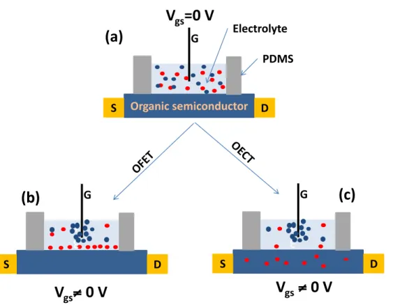
In an alternative device structure, an electronically insulating but ionically conducting electrolyte replaces the gate dielectric. The resulting device is known as electrolyte-gated transistor (Figure 1.9).[29,30] Electrolyte-gated (EG) transistors were first proposed in the 1950s.[31] In EG transistors, the application of a gate bias leads to the formation of an electrical double layer at the electrolyte/organic semiconductor interface.[32] The thin electrical double layer (few
nanometers) leads to a high capacitance (~10-20 µF/cm2) according the equation, C =! !
! where ε
is the permittivity, A is area of the electrode and D is the thickness of the double layer. Therefore, these transistors can be operated at low voltage (<2 V). EG transistors based on metal oxides, conducting polymers, organic semiconductors and carbon nanomaterials have been reported. EG transistors are studied for many different applications, especially in bioelectronics, drug delivery and diagnostics.[33-40]
Since conducting polymers and polycrystalline organic semiconductors cannot be considered completely impermeable to ions, current modulation in EG transistors can actually result from two gating (doping) mechanisms: electrostatic and electrochemical. To understand these mechanisms, we can adopt, initially, a simplified picture of an electrolyte included between two electrodes. When an electrical bias is applied between two electrodes immersed into an electrolyte, electrolyte ions move toward electrodes of opposite charge, driven by the electric field. For a transistor working under an electrostatic regime, with an applied gate bias, an electric double layer forms at the interface between the electrolyte and the channel. The corresponding devices are known as EG organic field-effect transistor (EG-OFET). By application of a gate voltage (Vgs), EDL form at the interfaces between the gate and the electrolyte and also between
the electrolyte and the channel (Figure 1.10b). This is the electrostatic mechanism. On the other hand, if the ions permeate the channel, an electrochemical dedoping/doping process takes place. This is the electrochemical mechanism of doping. The corresponding devices are known as organic electrochemical transistors (OECT) (Figure 1.10c).
Figure 1.10 Schematic representation of EG transistors and their subcategories, depending on the working mechanism (on the left the mechanism of doping is electrostatic, on the right it is electrochemical).
EG transistors (as all transistor types) can work in accumulation (or enhancement) or depletion mode. Transistors working in accumulation mode are in their OFF state (no or low current flowing between source and drain) when a gate bias (Vgs) is not applied and are turned ON upon
application of a gate voltage. Transistors working in depletion mode are in the ON state in absence of a gate bias applied and are turned OFF upon application of a gate bias. For a p-type channel working in accumulation mode, upon application of a negative Vgs, holes are
accumulated in the channel, due to the approach of anions at the interface between the electrolyte and the channel or the intercalation of anions into the channel. For p-type EG transistors working in depletion mode, by application of a positive Vgs, cations dedope the channel, decreasing the
hole density in the polymer. An analogous behavior (with opposite polarities of the electrical biases applied to the electrodes) is expected for n-type channels.
S D G 3 + S D G 3 + Organic semiconductor S D G
V
gs=0 V
V
gs≠ 0 V
V
gs≠ 0 V
(a)
(b)
Electrolyte PDMS(c)
1.5 Organic bioelectronic devices
Bioelectronics is defined as the studyand application of electronics in medicine and biology.[41] Bioelectronics involves interaction between electronic components (for example transistors and electrodes) and biological components such as enzymes, antibodies etc. as well as monitoring of bio-electric signals (e.g. heartbeat, brain or muscular activity). Bioelectronics devices such as biosensors and bioelectrodes have several applications in biological, chemical, health care, and environmental monitoring.[39,42-46]
Figure 1.11 Organic bioelectronics: biological moieties, including cells, micro-organisms, proteins, oligonucleotides, and small molecules, can be interfaced with organic electronics devices to yield biosensors, medical diagnostics, tools for biomedical research, and bioelectronic implants that will have a major impact in health care [41]. Reprinted with permission. Copyright © Materials Research Society 2010.
The scope of organic bioelectronics is shown in the schematics (Figure 1.11). Typical recognition elements (analytes) studied in biosensors are: enzymes, nucleic acids, antibodies, whole cells, and receptors collected from blood, urine, saliva, cell culture, food samples, and environmental samples. Transducers and bioreceptors are the main components of the biosensors. Bioreceptors are specific molecules/chemicals, to which the analyte specifically binds. Transducers are devices that translate the specific bioevents into measurable signals.
1.6 Supercapacitors
Supercapacitors (SCs) are promising energy storage devices, since they feature long cycling life, high power density, long shelf life.[47] SCs, also known as electrical double layer capacitors (EDLCs) or ultracapacitors, are intermediate to batteries and pure capacitors. SCs store more energy than capacitors, less energy than batteries, but deliver energy more rapidly than batteries and in a slower manner than capacitors. SCs were discovered in the early 1950s, during experiments on fuel cells and secondary batteries using porous carbon as the electrodes, and were patented in 1957.[48] Initially, SCs employed electrodes in sandwich configuration. Activated carbon coated on aluminum foil was the electrode material (the same for both electrodes), a porous separator was present between them and the electrolyte was liquid or solid. The Japanese company NEC Corporation first commercialized supercapacitors in 1971. At that time, SCs only had limited applications and were mainly used as back-up power supplies for volatile clock chips or computer memories.[49] The capacitance of first-generation SCs was mainly hampered by large internal equivalent series resistance (ESR), owing to the low conductivity of the electrodes and electrolytes. These problems were basically solved with improved electrode materials and the electrolytes by the 1980s. SCs were first used for military applications requiring high power density.[50] During the period from 1975 to 1981, B. E. Conway developed SCs using ruthenium oxide (RuOx) as electrode material.[51,52] This material can store electrostatic charges by the formation of electrical double layers and also generates a kind of “pseudocapacitance”. This means that reversible redox reactions involving electrosorption or intercalation take place at the electrode/electrolyte interface. Sulfuric acid was used as the electrolyte to ensure high specific capacitance (> 700 F/g) and low internal resistance.
The downsizing of SCs into micron scale can enable novel applications in autonomous, wireless microsensors and microelectronics. Photolithography can be used effectively to fabricate micro-supercapacitors (µSCs) in a planar, on-chip geometry. The energy storage and the devices to be powered can be integrated on a single chip, improving scalability and reducing cost.
Based on the working mechanism, supercapacitors are classified into: (i) electrical double layer capacitors (EDLC), in which the electrostatic charge accumulates between the electrode surface and the electrolyte interface, (ii) pseudocapacitors, where fast and reversible redox reactions (Faradaic processes) occur at the electrodes, and (iii) hybrid capacitors in which both processes
take place in a single device.
For EDLC, the capacitance is defined as:
C=ε0εrA D
where ε0 is the permittivity of free space, εr is the dielectric constant of the electrolyte, A is the
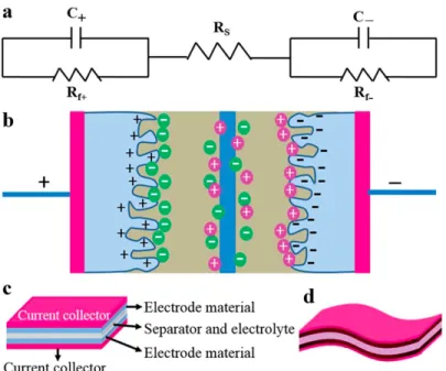
specific surface area of the electrode and D is the distance between the two electrodes. During charging/discharging of supercapacitors, a double layer forms at each of the two electrodes/electrolyte interfaces, so that the system can be treated as two capacitors connected in a series. (Figure 1.12) The cell capacitance (Ccell) of a capacitor can be calculated according to:
1 𝐶!"## = 1 𝐶!"#$%+ 1 𝐶!"#!!"#
where Canode and Ccathode represent the capacitance of the positive and negative electrode,
respectively.
Figure 1.12 (a) Equivalent circuit model for an electrochemical capacitor; b) Schematic representation of a two-electrode supercapacitor; (c) Schematic illustrations of the typical structure of a conventional supercapacitor (d) and its flexible counterpart.[53] Reprinted with permission. Copyright © 2014, Royal Society of Chemistry.
In the case of a symmetric device (with similar anode and cathode electrodes), the capacitance of the complete cell is half of the capacitance of each individual electrode. The specific capacitance of a supercapacitor cell can be calculated by cyclic voltammetry (CV), from the charge integrated from a cyclic voltammogram according to equation:
𝐶!"## = 𝑄 2𝑚𝑉 = 1 2𝑚𝑉𝜈 𝐼 𝑉 𝑑𝑉 !! !!
where Ccell is the specific capacitance of the cell (F/g), Q is the total charge (C), m (g) is the mass
of the active materials in each electrode, ν is the scan rate (V/s), and V+ and V- are the
electrochemical potentials of the positive and negative electrodes. For the galvanostatic charge discharge (GCD) method, the cell capacitance of a supercapacitor can be calculated from the charge–discharge curves from the following equation:
𝐶!"## =𝑚𝑑𝑉𝐼 𝑑𝑡
where I is the discharge current, m is the total mass of the active materials in the two electrodes and dV/dt is the slope of the discharge curve. The specific energy density (E, in Wh/kg) can be calculated according to:
𝐸 =3600𝑚𝐼 𝑉. 𝑑𝑡
The average specific power density (P, expressed in W/ kg) during discharge can be deduced from the specific energy density:
𝑃 = 𝐸 ∆𝑡
The maximum energy (Emax, in Wh/ kg) can be calculated according to:
𝐸!"# =
1
2𝐶!"##𝑉!
where V is the cell voltage or the cut-off voltage. The maximum power (Pmax, in W/kg) of a
supercapacitor is:
𝑃!"# = 𝑉! 4×𝐸𝑆𝑅
where the equivalent series resistance (ESR) is 𝐸𝑆𝑅 = ∆!
!! , with ∆V the initial drop in voltage
upon switching from charging to discharging.
1.7 Problem identification
OECT have attracted much interest for sensing and bioelectronics. However, the operating mechanism of an OECT, depending on doping/dedoping of the conducting polymer channel, is still under investigation. Hence, one of the key points in OECT research is to gain insight on the key parameters affecting the mechanism behind their operation.
Electroactive materials easily available from natural sources and biocompatible are particularly attractive for applications in bioelectronics. Melanin-based biopigments are a broad class of redox-active biopolymers found in living organisms. They are composed of macromolecular aggregates, mostly resembling polymer networks. Melanin-based biopigments exhibit unique optoelectronic properties including efficient photon–phonon conversion, mixed ionic-electronic conduction, redox activity, free radical scavenging, and cation chelation.[54-56] However, the structure-electroactivity relationships of melanin are still largely undiscovered.
1.8 General Objectives
The general objective of this Ph.D. thesis is the design, fabrication, and characterization of PEDOT:PSS organic electrochemical transistors and melanin supercapacitors.
For OECT, a better understanding of the doping/dedoping mechanism will pave the way to novel bioelectronics devices. Important issues that I addressed on OECTs are: i) the effect of the thickness of the channel on OECT modulation, ii) the influence of electrolyte ions on OECT modulation, iii) the influence of atmospheric oxygen on the performance of OECT and iv) influence of the gate material on the OECT performance.
To demonstrate proof of principles of melanin-based devices, I fabricated and characterized flexible melanin-based energy storage devices exploiting the redox activity and the proton transport properties of melanin. Besides the possible technological applications, this investigation
is expected to shed light on structure-electroactivity properties in biocompatible natural materials, well beyond the specific case of melanin.
1.8.1 Motivation
OECTs based on PEDOT:PSS show excellent electrochemical stability and reversibility and are therefore good candidates for applications at the interface with biology. Studying OECT requires a multidisciplinary approach, which includes knowledge in disciplines such as chemistry, device physics and biology.
Shedding light on their fundamental properties, in particular structural and electrochemical, is the premise to use natural materials, featuring desirable properties such as biocompatibility and biodegradability, for OECT or energy storage technological applications.
1.8.2 Specific objectives
To achieve the main objective, the following specific objectives need to be achieved:
I. Exploring the effect of the thickness of the channel of OECT on the device response.
Current modulation in OECT, unlike in field-effect transistors (where the doping is electrostatic and not electrochemical), involves the bulk of the polymer film, rather than the film/dielectric interfaces. Therefore it is important to understand how the thickness of the PEDOT:PSS channel affects the device characteristics. The goal of this study has been to find out how the current modulation varies for thin and thick films. This will shed light into the relationship between thickness of the active material and ON/OFF current ratio. To achieve this objective, we investigated the effect of the PEDOT:PSS channel thickness on OECT modulation using two different electrolytes: the cationic surfactant hexadecyltrimethylammonium bromide, also known as cetyltrimethylammonium bromide (CTAB), and NaCl. We employed cyclic voltammetry (CV) and electrochemical impedance spectroscopy (EIS) to gain insight into the impact of channel thickness, nature of the electrolyte and atmospheric oxygen on device performance.
II. Electrochemical study of the biomacromolecule melanin for application in supercapacitors
The synergy between the redox activity of the building blocks of melanin and the capability of several of their functionalities to reversibly bind electrolyte ions, constitutes the foundation for the use of melanin in pseudocapacitive energy storage systems. The goal of this work, has been to
exploit the energy storage properties of melanin in supercapacitor configuration. Our supercapacitors used melanin on carbon paper electrodes and aqueous electrolytes. Once the supercapacitors behavior was demonstrated, capitalizing on these results, we used an unconventional patterning approach to fabricate binder-free flexible micro-supercapacitors on plastic substrates. This study revealed that melanin can be an extremely attractive material for environmentally and human friendly energy storage solutions, because of its biocompatibility and biodegradability, combined with large availability and room temperature processing.
III. Conducting Polymer Transistors Making Use of Activated Carbon Gate Electrodes
The specific surface area of gate electrodes has an important effect on the performance of OECT, both on the transistor modulation and the gate electrical bias. We introduced the high surface activated carbon (AC) as the gate electrode for OECT. We investigated the performance of OECT based on PEDOT:PSS using AC gate electrodes.
1.9 Organization of the work
This thesis is organized into eight Chapters. Chapter 1 includes an overview of the topics related to the subjects (organic electronics, organic transistors, conducting polymers, organic bioelectronics, supercapacitors), problem identification and objectives of the thesis. Chapter 2 introduces conducting polymers (in particular PEDOT:PSS), the general working mechanism of OECT, a literature survey of OECT, energy storage property of melanin-based supercapacitors. Chapters 3 and 4 correspond to two articles (articles 1 and 2) of which I was the first author. Chapter 5 contains excerpts of an article where two of my colleagues and I contributed equally as first authors (article 3). Chapter 6 is about the “electrochemistry of melanin”.
Article 1: Effect of channel thickness, electrolyte ions, and dissolved oxygen on the performance of organic electrochemical transistors (Published in Applied Physics Letters).
Article 2: Melanin-based flexible supercapacitors (Published in the Journal of Materials Chemistry C).
Excerpts from Article 3: Conducting Polymer Transistors Making Use of Activated Carbon Gate Electrodes (Shared first author article) (Published in ACS Applied Materials and Interfaces).
The following paragraphs describe how these articles contribute to the objectives of the thesis. In article 1, we investigated the device characteristics of OECT based on thin films of PEDOT:PSS. We employed various channel thicknesses and two different electrolytes: the micelle forming surfactant cetyltrimethyl ammonium bromide (CTAB) and NaCl. The highest ON/OFF ratios were achieved at low film thicknesses using CTAB as the electrolyte. Cyclic voltammetry suggests that a redox reaction between oxygen dissolved in the electrolytes and PEDOT:PSS leads to low ON/OFF ratios, mostly when NaCl is used as the electrolyte. From cyclic voltammetry and electrochemical impedance spectroscopy reveals that doping/ dedoping of the channel becomes slower at high film thickness and in the presence of bulky ions. Article 1 has been published in Applied Physics Letters (2015, 107, 053303(1)- 053303(5)).
In article 2, we used the pseudocapacitive properties of melanin for energy storage systems. We demonstrated supercapacitors and flexible micro-supercapacitors making use of electrodes based on the biocompatible and biodegradable pigment melanin, working in aqueous electrolytes. Melanin-based supercapacitor electrodes are fabricated at room temperature, by easy solution processing, without the need of a high-temperature treatment, unlike the large majority of supercapacitors based on biopolymer-derived electrodes reported to date. In slightly acidic media, a gravimetric specific capacitance as high as 167 F/g was observed for melanin-based electrodes on carbon paper. Further, we demonstrated a binder-free micro-supercapacitor fabricated on flexible polyethylene terephthalate (PET). The microfabrication was performed by unconventional lithography based on ParyleneC patterning. Our flexible micro-supercapacitors showed a power density of 5.24 mW/cm2 and a specific capacitance of 10.8 F/g.
Article 3 is a shared first author article. My contribution to this article has been included in the thesis. The characteristics of the gate electrode have significant effects on the behavior of OECT, which are intensively investigated for the applications in the booming field of organic bioelectronics. In this work, high specific surface area activated carbon (AC) was used as gate electrode material in OECT based on the conducting polymer PEDOT:PSS. We found that the high specific capacitance of the AC gate electrodes leads to high drain-source current modulation in OECT at low voltage, compared to PEDOT:PSS gate electrodes of comparable geometric area. Article 2 has been published in ACS Applied Materials and Interfaces (2015, 7, 969−973).
![Figure 1.5 The molecular structure of a few technologically relevant conjugated polymers and their electronic band gap.[17]](https://thumb-eu.123doks.com/thumbv2/123doknet/2334547.32494/28.918.120.713.109.752/figure-molecular-structure-technologically-relevant-conjugated-polymers-electronic.webp)
![Figure 1.7 Schematic illustration of an OPV cell (a) I–V characteristics of a PV cell under dark (blue) and illumination (red) conditions (b) Schematic illustration of photocurrent generation processes for the OPV cells (c) [25] Reprinte](https://thumb-eu.123doks.com/thumbv2/123doknet/2334547.32494/31.918.213.619.102.463/schematic-illustration-characteristics-illumination-schematic-illustration-photocurrent-generation.webp)

![Figure 2.4 Chemical polymerization of ethylenedioxythiophene in the presence of polystyrenesulfonic acid.[61]](https://thumb-eu.123doks.com/thumbv2/123doknet/2334547.32494/48.918.279.528.116.344/figure-chemical-polymerization-ethylenedioxythiophene-presence-polystyrenesulfonic-acid.webp)
![Figure 2.5 (a) Device structure and electrical circuit of a PEDOT:PSS OECT; (b and c) OECT working principle; circles filled with - indicate PSS − ions and + indicate mobile holes.[91] Reprinted with permission](https://thumb-eu.123doks.com/thumbv2/123doknet/2334547.32494/50.918.272.620.421.923/device-structure-electrical-principle-indicate-indicate-reprinted-permission.webp)