DOCTORAT DE L'UNIVERSITÉ DE TOULOUSE
Délivré par :Institut National Polytechnique de Toulouse (Toulouse INP) Discipline ou spécialité :
Génie Electrique
Présentée et soutenue par :
M. YAZAN BARAZIle jeudi 1 octobre 2020
Titre :
Unité de recherche : Ecole doctorale :
Fast short-circuit protection for SiC MOSFETs in extreme short-circuit
conditions by integrated functions in CMOS-ASIC technology
Génie Electrique, Electronique, Télécommunications (GEET)
Laboratoire Plasma et Conversion d'Energie ( LAPLACE) Directeur(s) de Thèse :
M. NICOLAS ROUGER M. FREDERIC RICHARDEAU
Rapporteurs :
M. JEAN-CHRISTOPHE CREBIER, INP DE GRENOBLE M. NICOLAS GINOT, UNIVERSITE DE NANTES
Membre(s) du jury :
M. JEAN-CHRISTOPHE CREBIER, INP DE GRENOBLE, Président M. FREDERIC RICHARDEAU, TOULOUSE INP, Membre M. HASSAN MAHER, UNIVERSITE DE SHERBROOKE, Membre
M. MARC COUSINEAU, TOULOUSE INP, Membre
Mme MOUNIRA BERKANI, ECOLE NORMALE SUPERIEURE PARIS-SACLAY, Membre M. NICOLAS ROUGER, TOULOUSE INP, Membre
M. STÉPHANE AZZOPARDI, GROUPE SAFRAN, Membre M. THIERRY SICARD, , Invité
P h D t h e s i s o f B a r a z i Y a z a n P a g e 2 | 225
Acknowledgement
(Remerciement)
Je suis très honoré d'avoir pu mener mes travaux de thèse (financés par le Ministère de l'Enseignement supérieur, d la recherche et de l’innovation) au sein du laboratoire Laplace où j'ai eu la chance de collaborer avec de nombreuses personnes passionnées et très impliquées dans leur travail.
Je tiens en premier lieu à exprimer toute ma reconnaissance et ma gratitude à mes encadrants de thèse, Nicolas Rouger et Frédéric Richardeau, pour leur implication et leur soutien sans faille dans l’élaboration et la réussite de cette thèse. Je tiens à remercier ces derniers individuellement, pour leurs qualités professionnelles et leur dévouement à toute épreuve. Ils ont toujours été à l'écoute et disponibles pour me guider tout au long de ces trois ans. Nos interactions étaient toujours très riches et m'ont permis de progresser et d'apprendre à chaque fois un peu plus. Je tiens également à souligner leurs qualités humaines, merci pour ces trois belles années.
Je remercie les membres de ce jury de thèse à qui j'ai eu le privilège de présenter mes travaux. Tout d'abord je remercie Jean-Christophe Crebier de m’avoir fait l’honneur de présider le jury. Je remercie également Nicolas Ginot et Jean-Christophe Crebier d’avoir accepté d’être rapporteur de mon manuscrit. Je remercie ensuite Marc Cousineau, Mounira Berkani, Hassan Maher, Stéphane Azzopardi, Thierry Sicard d'avoir accepté d'examiner ma thèse. L'ensemble des discussions que nous avons pu avoir ont été très riches et intéressantes. J'ai été profondément touché par vos appréciations et commentaires, je vous en suis très reconnaissant.
Je remercie également l'ensemble des personnes avec qui j'ai été amené à travailler, notamment Jean-Marc Blaquières et Sébastien Vinnac, ingénieurs du laboratoire LAPLACE, avec qui le travail était toujours très agréable et dont l'implication fut essentielle et indispensable pour la mise en oeuvre et la genèse des prototypes et de mes travaux en général. Nous avons passé de bons moments, merci.
Je tiens à remercier également les membres du laboratoire Laplace pour leur aide et leur bienveillance pour ceux que j'ai côtoyé durant ces trois années de thèse, en particulier les membres du groupe CS. Merci également à Jessica Toscano et Ariane Arnaud pour leur précieuse aide concernant toutes les démarches administratives.
Je remercie l’ensemble de mes collègues de bureau avec qui j'ai créé de véritables liens d'amitié au-delà même du travail : François Boige, Plinio Bau, Wadia Jouha, Amirouche Oumaziz.
P h D t h e s i s o f B a r a z i Y a z a n P a g e 3 | 225 Je remercie les membres de l’ADeL 2020 et les membres du bureau 2019, avec qui j'ai passé de bons moments. Maxime, Davin, Timothé, Laura, merci pour tous ces moments de convivialité partagés ensemble.
Je remercie enfin tous mes collègues avec qui j'ai pu partager des enseignements, Nicolas Roux, Philippe Ladoux, Marc Cousineau, Jonathan L., Rémi B., Yann G., Olivier L., François P., Hadi. Je remercie ensuite tous mes amis et collègues de laboratoire pour tout ce que l'on aura partagé au cours de ces trois ans, Mohsin, Abdulrahman, Kepa, Miguel, Najoua, Andrea E., Davin, Mathieu, Olivier, Francois, Rémi, Jonathan, Timothé, Hugo, Andrea V., Thomas, Youness, Quentin, Grégoire, Bernard, Vinicius, Joseph, Jordan, Sami, Yann.
Last but not least, mes chaleureux remerciements à toute ma famille pour leur soutien durant ma thèse. Special thanks to my homies Adil Brik, Ahmed Alami, Albraq Barazi.
P h D t h e s i s o f B a r a z i Y a z a n P a g e 4 | 225
To my Mom
P h D t h e s i s o f B a r a z i Y a z a n P a g e 5 | 225 Table of Contents THÈSE ... 0 Acknowledgement ... 2 Table of Contents ... 5 List of Acronyms ... 8 Résumé ... 9 Abstract ... 11
Chapter I: Challenges associated with driving SiC MOSFETs ... 14
Introduction ... 14
Specificities of SiC MOSFETs ... 15
Wide-band gap power devices evolution... 15
Electrical and switching characterization of SiC MOSFET ... 18
Switching mechanism analysis ... 21
Gate Drivers for SiC FETs ... 25
Gate Drivers fundamentals for power FETs ... 26
Gate driver functions ... 26
Gate driver fundamental parameters... 28
Isolation ... 29
Buffer Architecture ... 32
SiC MOSFET power device and the challenges faced by the gate driver ... 34
Switching and transmission monitoring ... 36
Health monitoring ... 39
Safety monitoring ... 40
Technology review ... 43
Behavior of SiC MOSFET Under Short-Circuit ... 48
Characteristics impacts of SiC MOSFET and Si IGBT under short-circuit ... 48
Turn-on analysis of SiC MOSFET ... 50
Normal Turn-on ... 50
Hard Switch Fault ... 52
Fault under load ... 53
Unique SiC MOSFET behavior under Short-circuit ... 53
Possible Failure mode ... 54
Short-Circuit Detection techniques ... 56
P h D t h e s i s o f B a r a z i Y a z a n P a g e 6 | 225
Sense-Fet monitoring method... 58
Current transformer monitoring method ... 58
Desaturation monitoring method ... 58
Gate current leakage monitoring method ... 60
Gate Charge monitoring method ... 61
Fault detection methods Summary / Benchmark ... 64
Conclusion ... 65
Chapter II: Design of integrated gate drivers in 0.18µm SOI CMOS technology for MOSFET SiC power device ... 67
Introduction ... 67
Design of the power test benches ... 67
Power Test bench V1 ... 68
Power Test bench V2 ... 69
CMOS technology and Buffer specification ... 70
SOI CMOS 0.18 µm Technology ... 71
Bulk CMOS vs SOI CMOS ... 71
0.18 Micron Modular BCsD-on-SOI Technology ... 72
Buffer Specifications and adaptation ... 73
Buffer Architecture & Technology options ... 76
Design and sizing of an integrated active gate driver ... 78
Active gate driver Architecture ... 79
Level shifter ... 79
Output Buffer ... 81
Active Miller Clamp (AMC) ... 89
High impedance and Soft shut down ... 93
Summary of the Gate driver ... 95
Gate driver layout design & packaging ... 95
Characterization and experimental validation of the gate driver ... 101
V0.A under a load capacitor with no power ... 101
V2.A implementation in the power test bench V2 ... 107
Modular Multilevel Gate driver MMAGD ... 108
MMAGD topology ... 109
MMAGD design and layout ... 113
Conclusion ... 116
P h D t h e s i s o f B a r a z i Y a z a n P a g e 7 | 225
Introduction ... 118
Gate charge monitoring ... 119
Analytical study of the Gate charge ... 119
Normal Turn-on condition ... 119
Hard switch Fault condition ... 122
Fault under load condition ... 125
Open Circuit condition ... 126
Gate charge robustness study ... 128
Proposed schematic, RC rating and trade-off ... 132
Experimental results ... 137
V1.A Discrete components prototype ... 137
V1.b SMD prototype ... 143
Gate Derivation Monitoring ... 146
Proposed schematic & review of the method ... 147
Slope approach ... 149
Dip approach ... 150
Detection circuit based on derivation monitoring and simulation behavior ... 151
Design and layout of the derivation method ... 155
Experimental results ... 163
Experimental results under an equivalent capacitor and no power, V0.1... 163
Experimental results using a DUT and power test bench, V2.2 ... 164
Feedback from power FET to CMOS: Third monitoring method ... 167
Comparison between the proposed detection techniques ... 168
Conclusion ... 170
Conclusion & Outlook ... 172
Appendix A ... 175 Appendix B ... 178 Appendix C ... 180 List of Figures ... 205 List of Tables ... 210 References ... 212 Author's references ... 224
P h D t h e s i s o f B a r a z i Y a z a n P a g e 8 | 225
List of Acronyms
Si Silicon
WBG Wide Band Gap
SiC Silicon Carbide
GaN Gallium Nitride
MOSFET Metal Oxide Semiconductor Field Effect Transistor
SiO2 Silicon dioxide
SJ-MOSFET Super-Junction MOSFET
JFET Junction-Field Effect Transistor
IGBT Insulated Gate Bipolar Transistor
HEMT High-Electron-Mobility Transistor
GTO Gate Turn-Off Transistor
DUT Device Under Test
BJT Bipolar Junction Transistor
HV High voltage
LV Low voltage
HS High side
LS Low side
EMI Electro-Magnetic Interference
EMC Electro-Magnetic Compatibility
CMTI Common Mode Transient Immunity
HT High temperature
EV Electric vehicle
PWM Pulse Width Modulation
AGD Active Gate Driver
MMAGD Multi-level Modular Active Gate Driver
CMOS Complementary metal–oxide–semiconductor
PMOS P-type metal–oxide–semiconductor
NMOS N-type metal–oxide–semiconductor
SC Short-Circuit
HSF Hard Switch Fault
FUL Fault Under Load
OC Open Circuit
DESAT Desaturation
ASIC Application-Specific Integrated Circuit
SMD Surface Mounted Diode
PCB Printed Circuit Board
DRC Design Rule Checking
LVS Layout Versus Schematic
FPGA Field programmable gate arrays
SOI Silicon On Insulator structure
AMC Active Miller Clamp
SSD Soft Shut Down
P h D t h e s i s o f B a r a z i Y a z a n P a g e 9 | 225
Résumé
Le manuscrit est rédigé en anglais, vous pouvez trouver un résumer de l’ensemble de la thèse à l’Annexe C. Les transistors de puissance grands gaps tels que les MOSFETs SiC et HEMT GaN repoussent les compromis classiques en électronique de puissance. Brièvement, des gains significatifs ont été démontrés par les transistors SiC et GaN: meilleurs rendements, couplés à une augmentation des densités de puissance offertes par la montée en fréquence de découpage. Les MOSFET SiC à haute tension présentent des spécificités telles qu'une faible tenue en court-circuit (SC) par rapport aux IGBT Si et un oxyde de grille aminci, et une tension de commande rapprochée grille-source élevée. La polarisation négative sur la grille à l'état bloqué crée un stress supplémentaire qui réduit la fiabilité du MOSFET SiC. La forte polarisation positive de la grille provoque un courant de saturation de drain important en cas de SC. Ainsi, cette technologie fait émerger des besoins spécifiques de surveillance et de protection ultra-rapides. Pour cela, le travail de cette thèse se focalise sur deux études pour surmonter ces contraintes
toute en gardant un bon compromis de performances entre « niveau d’intégration technologique ‘CMS/ASIC-CMOS’–rapidité–robustesse ». La première, regroupe un ensemble de solutions nouvelles permettant une détection du court-circuit sur le cycle de commutation, sur la base
d'une architecture conventionnelle de commande rapprochée dite à 2 niveaux de tension. La deuxième étude est plus exploratoire et basée sur une nouvelle architecture de gate–driver,
dite multi-niveaux, à faible niveau de stress pour le MOSFET SiC tout en maintenant les
performances dynamiques.
Les travaux portent tout d’abord sur l’environnement du SiC MOSFET, (caractérisation et propriétés de comportement en SC par simulations orientées "circuit" de type PLECS™ et LTSpice™), puis présentent une étude bibliographique sur les commandes rapprochées dites Gate Driver, une étude approfondie a été réalisée sur les court-circuits type I & II (Hard switch fault) (Fault under Load) ; regroupés dans un premier chapitre du manuscrit.
Un banc de test réalisé antérieurement au sein du laboratoire, a permis de compléter et de valider l’étude d'analyse-simulation et de préparer des stimuli test pour l'étape de conception des nouvelles solutions.
Inspirée par la méthode de Gate charge apparue pour les IGBTs en silicium et évoquée pour les MOSFETs SiC, cette première approche fait l'objet d'un travail de conception, de dimensionnement et de prototypage. Cette méthode de référence permet une détection de type HSF en moins de 200ns sous 0-600V avec des composants 1,2kV allant de 80 mOhm à 120mOhm.
S'agissant des nouvelles méthodes de détection rapides et intégrées, les travaux de cette thèse se focalisent particulièrement sur la conception d’un circuit ASIC CMOS. Pour cela, la conception d’un gate driver adapté est essentiel. Un ASIC est conçu en technologie X-Fab
P h D t h e s i s o f B a r a z i Y a z a n P a g e 10 | 225 0,18µm SOI-CMOS sous Cadence™, et puis mis en boitier et assemblé sur PCB conçu pour les besoins de tests et adaptable au banc principal. La conception du gate driver a considéré de nombreuses fonctions (détection du SC, SSD Soft shut down, buffer segmenté, AMC Active Miller Clamp", …). Du point de vue de la détection du SC, les fonctions nouvelles de surveillance intégrées concernent la méthode de dérivation temporelle de VGS qui est basée sur une détection par un circuit dérivateur analogique RC sur la séquence de plateau avec deux variantes. Une deuxième méthode nouvelle partiellement intégrée dans l'ASIC a été conçu, non développé dans ce mémoire dans le but d’une valorisation.
En marge de cette étude principale, une étude exploratoire a porté sur une nouvelle architecture modulaire de commande rapprochée à plusieurs niveaux de tension de polarisation tirant profit de l'isolation SOI et des transistors CMOS à basse tension pour piloter le MOSFETs SiC et améliorer leur fiabilité grâce à une sélection active et dynamique à plusieurs niveaux sur les séquences de commutation et les états marche/arrêt.
P h D t h e s i s o f B a r a z i Y a z a n P a g e 11 | 225
Abstract
Wide band gap power transistors such as Silicon Carbide (SiC) MOSFETs and High Electron Mobility Transistors (HEMTs) Gallium Nitride (GaN) push furthermore the classical compromises in power electronics. Briefly, significant gains have been demonstrated by SiC and GaN transistors: better figure of merit, coupled with an increase in power densities offered by the increase in switching frequency. High-voltage SiC MOSFETs have specific features such as a low short-circuit withstand time capability compared to Si IGBTs, a thinner gate oxide, and a higher gate-to-source switching control voltage. The negative bias on the gate at the off-state creates additional stress which reduces the reliability of the SiC MOSFET. The high positive bias on the gate causes a large drain saturation current in the event of a short-circuit. Thus, this technology gives rise to specific needs for ultra-fast monitoring and protection. For this reason, the work of this thesis focuses on two studies to overcome these constraints. The first one, gathers a set of new solutions allowing a detection of the short-circuit on the switching cycle, based on a conventional switch control architecture with two voltage levels. The second study is more exploratory and is based on a new gate-driver architecture, called multi-level, with low stress level for the SiC MOSFET while maintaining dynamic performances. These studies were conducted with the objective of reaching a good performance compromise between “SMD/ASIC-CMOS technological integration level - speed – robustness”.
The first chapter of the manuscript covers firstly the SiC MOSFET environment, (characterization and properties of short-circuit behavior by simulation using PLECS and LTSpice software) and covers secondly a bibliographical study on the Gate drivers. At last, an in-depth study was carried out on type I (Hard Switch Fault, HSF) and type II (Fault Under Load, FUL) short-circuits, as well as detection circuits proposed in the literature. Most of these detection circuits are insufficient as they do not achieve and allow the above performance compromise.
A test bench, previously carried out in the laboratory, was used to complete and validate the analysis-simulation study and to prepare test stimuli for the design stage of new solutions. In order to remain in the low-voltage environment of the gate driver, the problems were treated directly and solely exploiting the gate voltage and current of the SiC MOSFET. Inspired by the Gate charge method that appeared for Si IGBTs and evoked for SiC MOSFETs, our effort was initially directed towards this method as a reference. This method has therefore been the subject of design, dimensioning and prototyping work. This reference allows an HSF type detection in less than 200ns under 400V with 1.2kV components ranging from 80m to 120m.
Regarding new rapid and integrated detection methods, the work of this thesis focuses particularly on the design of a CMOS ASIC circuit. For this, the design of an adapted gate driver is essential. An ASIC is designed in X-Fab XT-0.18 SOI-CMOS technology under Cadence, and then packaged and assembled on a PCB. The PCB is designed for test needs and adaptable to the main bench. The design of the gate driver considered many functions (short-circuit detection, soft-shut-down, segmented buffer, an "Active Miller clamp", ...). From the
P h D t h e s i s o f B a r a z i Y a z a n P a g e 12 | 225 short-circuit detection point of view, the new integrated monitoring functions concern the VGS time derivative method which is based on a detection by an RC analog shunt circuit on the plateau sequence (VGS above VGS_M) with two approaches: the first approach is based on a dip detection, i.e. the presence or not of the Miller plateau. The second approach is based on slope detection, i.e. the variability of the input capacitance of the power transistor under short-circuit HSF compared to normal operation. These methods are compared in the third chapter of the thesis, and demonstrate fault detection times between 40ns and 80ns, and preliminary robustness studies and critical cases are presented. A second new method is partially integrated in the ASIC, was designed. This method is not developed in the manuscript because it is confidential.
In addition to the main study, an exploratory study has focused on a modular architecture for close control at several bias voltage levels taking advantage of SOI isolation and low voltage CMOS transistors to drive SiC MOSFETs and to improve their reliability through active and dynamic multi-level selection of switching sequences and on/off states. This work is presented in the second chapter of the manuscript.
P h D t h e s i s o f B a r a z i Y a z a n P a g e 13 | 225
Chapter I: Challenges associated with
P h D t h e s i s o f B a r a z i Y a z a n P a g e 14 | 225
Chapter I: Challenges associated with driving SiC MOSFETs
In this first chapter, we describe a brief overview of the state of the art of power transistors. As well, an overview of the power device, gate drivers; and the challenges faced by the gate driver for SiC power devices is presented. Thus, the functions of monitoring and control around power transistors are discussed. Thus, an insightful study of the state of the art of
short-circuit behavior and detection methods is developed.
Introduction
The activities of power electronics consist of providing the capability to transfer energy to one or more electrical loads from one or more primary energy sources. In order to be able to control, modulate and transfer energy, power converters need to use at least one controlled power switch. For this purpose, there is a wide range of switches in silicon technology (GTO-Thyristor, IGBT, MOSFET), as well as, wide band gap semiconductor components (SiC, GaN) available from various manufacturers and research institutes. Insulated gate transistors such as the MOSFETs or IGBTs must be driven by a control circuit, called gate driver. The purpose of the gate driver circuit is to provide, control and manage the charge and/or discharge of the gate electrode of the power transistor, and to allow changes of state (from On to Off or vice versa). Wide bandgap semiconductor materials, such as Silicon Carbide (SiC), have undergone a tremendous evolution in recent years. Power semiconductor devices, such as Insulated Gate Bipolar Transistors (IGBTs) and Super-Junction (SJ-MOSFET) silicon devices, are limited in terms of maximum switching speeds and more generally, with figures of merit close to the theoretical limits of Silicon [1]. Consequently, silicon power devices have high switching losses and large and expensive thermal management systems, leading to limits in terms of maximum converter efficiency and switching frequency. In contrast, SiC MOSFETs are promising power semiconductor devices for high density converters, with low conduction and switching losses and high temperature stability [2].As the SiC MOSFETs gain maturity and their cost goes down with time, SiC MOSFETs are expected to be adapted and used in more and more applications. However, the higher power densities enabled brings the issue of how long a short-circuit fault can be sustained by a SiC power device. Regardless of the short-circuit robustness, the short-circuit fault must be turned OFF as soon as detected to preserve the device from degradation and possible repeated short-circuit occurrences.The short-circuit (SC) delay time capability for SiC MOSFETs is lower than for silicon devices [3]. Power converters designed with these components are therefore less robust.
Power semiconductors devices are used in various industrial applications, including motor drives, battery chargers, switch mode power supplies and converters. These devices are exposed to several types of short-circuit (SC). The hard switch fault (HSF, SC type I) and fault under load (FUL, SC type II) are the two main fault behaviors. Safety is necessary for these typical applications.
P h D t h e s i s o f B a r a z i Y a z a n P a g e 15 | 225 In order to fully design a gate driver with different functions oriented protection and safety, dedicated for SiC MOSFETs, the electrical characterization of SiC MOSFET is mandatory. Gate driver fundamentals and their key requirement are presented. Different architectures of the gate driver are proposed, for the purpose to get fully familiar with the environment of the SC detection functions.
A clear and detailed comparison between SiC MOSFET and Si IGBT behavior under short-circuit is presented in this chapter. As well as, the two main fault types HSF and FUL are developed. Different monitoring and protection methods for SiC MOSFETs are investigated and developed. The aim is to establish how fast a short-circuit fault can be detected and how fast it can be turned OFF. Therefore, detailed analyses and comparisons between the SC detection methods are presented.
Specificities of SiC MOSFETs
In this section, the evolution of the power devices is introduced. This evolution shows how the market is oriented towards new wide band-gap (WBG) devices. Wide band-gap transistors have significant advantages and offer new market opportunities. In order to benefit from the opportunities offered by the new WBG components, their implementation must be carefully studied within the power circuit and in association with their gate drivers.
In this section as well, detailed analysis of the switching mechanisms will be introduced of a power inverter cell consisting of SiC MOSFETs. This analysis will allow us to highlight the main physical parameters and freedom degrees to consider in order to optimize the switching sequences by the gate driver.
Wide-band gap power devices evolution
Power semiconductor devices are used to control the energy transfer of electronic systems. Over the last two decades the technology of power semiconductors has made impressive progress.Power transistors are mainly classified into two types [4] [5] :
Unipolar components Field Effect Transistors (FET): such as the JFET (Junction-Field Effect Transistor) or MOSFET (Metal-Oxide-Semiconductor Field Effect Transistor) or the schottky-diode; where only one type of carrier circulates in the component (majority carriers). The FET transistors have control on the size and shape of a channel between source and drain which is created by applied voltage [6].
Bipolar components: such as PIN diode, IGBT (Insulated-Gate Bipolar Transistor); where for IGBTs have both types of carriers circulate in the component. The name itself indicates that it has two junctions between p-type and n-type semiconductors.
Fig.I. 1 shows the large families of Silicon power components. They are distributed regarding their power and frequency operation range. Each type has its advantages and disadvantages, which respond to different application areas, [7].
The new generations of power converters are based on higher power densities, higher efficiencies and greater robustness. In addition to this, they are based on even faster operation,
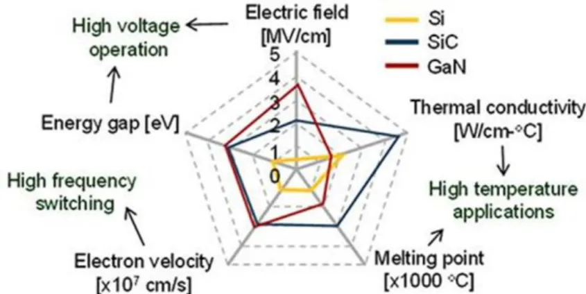
P h D t h e s i s o f B a r a z i Y a z a n P a g e 16 | 225 low conduction and switching losses and higher temperatures operation. While the converter topology may vary depending on the application, the typical specifications are to process power in an efficient manner, safely, and at low cost. Commonly, the semiconductor devices have been made with silicon (Si) (narrow band semiconductors). However, this leads the semiconductors to adapt and to gain maturity in order to meet those criteria. For a while, silicon devices face its limits, unless new breakthroughs are identified. Therefore, wide band-gap (WBG) semiconductors take place by their different advantages, cited above [8]. The large energy separation between the conduction and the valance bands allows these devices to operate theoretically at elevated temperatures and at critical electrical field, Fig.I. 2.
Fig.I. 1. Application areas of classical discrete power semiconductors [9].
The first silicon carbide (SiC) power device to become commercially available in 2001 is the SiC--Schottky-diode mostly used in power supply application [10]. The WBG devices are out of the laboratories and into the real world. In particular, SiC, and Gallium Nitride (GaN) have led to tremendous advances in power switching and/or power amplifier applications [11]. Nowadays, SiC MOSFETs are commonly found in several areas (Rail, motor drive, PV, etc ), and GaN power transistors have found applications in 600V market segments such as data center server power supplies [8] [12] .
SiC attracts attention as material for power devices because of its high thermal capability, high carrier mobility and high critical electric field before avalanche breakdown. Also, SiC is the only compound semiconductor whose native oxide is silicon dioxide (SiO2), the same insulator as Si. The SiO2 has good performance as passivation film in Si power devices, so that this makes it possible to fabricate the entire MOS-based devices in SiC. The main advantage of SiC semiconductor device is the very low resistance of the drift region even if it is designed to
P h D t h e s i s o f B a r a z i Y a z a n P a g e 17 | 225 support higher voltage [13]. This favors the development of high voltage unipolar devices which have much superior switching speed than bipolar devices. Also, much lower resistance of the drift region in SiC could enable the development of SiC high power devices [14]. However, the channel region of SiC power transistors still remains an issue due to interface traps and the consequent degradation on the channel-mobility, threshold-voltage drift, whereas the channel resistance is not negligible even for high voltage SiC MOSFETs.
𝑅𝑆𝑝𝑒𝑐𝑖𝑓𝑖𝑐[ . 𝑐𝑚2] = 4 ∗ 𝑉𝐵𝑅2 µ𝑁OrEc3 𝐸𝑠𝑤𝑖𝑡𝑐ℎ𝑖𝑛𝑔[𝐽] =1 2∗ 𝑉 ∗ 𝐼 ∗ 𝑄𝐺 𝑖𝐺_𝐷𝑟𝑖𝑣𝑒 (I. 1)
Fig.I. 2. Material properties of Silicon, Silicon Carbide and GaN
Reducing the channel resistance has a direct impact on increasing the area of the semiconductors.The reduction in parasitic capacitances also results in a lower driving energy and a higher switching speed of the component in nominal operation by agreeing to manage the EMC issue. In the event of a short-circuit, however, the high channel polarization will impose a very high short-circuit current-density which, due to the small chip area, will rapidly heat up the component to an extreme value especially for medium and high voltage device. This effect can be exacerbated on the decreasing threshold voltage in a very low negative bias just before the short-circuit event. This property is further enhanced by the presence of a short-channel in many MOSFET SiC structures, which further reduces the on-state resistance but increases the high-voltage drain-source dependency unlike Si device. The behavior study of SiC MOSFETs under short-circuit is detailed in the chap.I.4.
∆𝑇𝑗(𝑡) = 2. 𝑉𝑑𝑠.𝐽𝑠𝑎𝑡 √𝜋𝜌𝜆𝐶𝑝
√𝑡𝑆𝐶
P h D t h e s i s o f B a r a z i Y a z a n P a g e 18 | 225 Eq.(I. 2) represents a simplified adiabatic 2D junction temperature transient from idealized
constant SC [15]. Note that SiC chip exhibits higher “SC JSat (A/mm²)” than Si chip + thinner epi N- layer than Si TSC-SiC << TSC-Si.
Electrical and switching characterization of SiC MOSFET
A MOSFET (type of FET) is a voltage-controlled device easy to control. It uses an electric field to control the shape and hence the electron conductivity through the channel in a semiconductor material. The circuit symbol of an n-channel inversion MOSFET is shown in Fig.I. 3.(a). The equivalent circuit model used for the analysis of MOSFET switching performance is presented in Fig.I. 3 .(b). When the MOSFET is used as a switch, its basic function is to control the drain to source current or impedance by the gate voltage. MOSFET transistors require the continuous application of a gate-source voltage of appropriate magnitude in order to be in the on state. There is no gate current flow except during the switching of the transistor from on to off or vice versa. Nowadays, the switching times are very short, being in the range of few nanoseconds or few tens of nanoseconds, depending on the size of the chip and the gate device capability. The idealized characteristics of the device operating as a switch is shown in Fig.I. 3.(c) [16].
Fig.I. 3. N-channel MOSFET, (a). Symbol (b). Equivalent circuit (c). Idealized ID-VDS characteristics (d). Transfer ID-VGS characteristic.
The equivalent circuit shows parasitic components that have the greatest effect on the switching characteristics. The switching performance of a device is determined by the time required to establish voltage changes across the input capacitance 𝐶𝑖𝑠𝑠 = 𝐶𝐺𝑆 + 𝐶𝐺𝐷. RG_int is the internal gate resistance, approximate inversely proportional to active area. LS and LD are
P h D t h e s i s o f B a r a z i Y a z a n P a g e 19 | 225 source and drain lead inductances; they are equivalent to few nH. They are involved in the power loop of the circuit. In the other hand LG, not taken into consideration in the figure, gets involved in the switching behavior. Those values can increase dramatically depending on the used package and interconnection techniques.
The SiC MOSFET – PIN body diode has low recovery charges, resulting in ultralow switching losses but has higher forward voltage. This is due to the fact that the bandgap of SiC is 3 times larger than that of Si. So it will generally only be used for dead-time sequence. Designs based on Schottky body-diode, are also proposed but not yet commercialized on many references. The diode forward voltage is the guaranteed maximum forward drop of the body-drain diode at a specified value of source current.
The on-state resistance RDS_ON is not presented in the equivalent circuit between the drain and the source. This resistance is a representation of the ohmic losses, which arises from the drain drift region. Also, ohmic losses in the channel are included in the RDS_ON value.
Briefly, the gate-source controlled drain-source current source shown in the equivalent circuit is equal to 0 before VGS reaches Vth and then proportional, for high VGS polarization, to gfs(VGS-Vth). On Fig.I. 3. (d). the transfer curve is presented. As shown the MOSFET is in cutoff when the gate-source VGS is below the threshold voltage Vth. The value of the threshold voltage is around a few volts for most power MOSFETs but, due oxide traps, a drift of several hundred mV can be seen in operation depending on the levels of gate polarization, duty cycle and switching frequency.The device is under open-circuit operation and must hold off the power supply voltage applied to the circuit. This means that the drain-source breakdown voltage BVDSS must be larger than the applied VDS to avoid breakdown and the attendant high power dissipation. When breakdown occurs, it is due to the avalanche breakdown of the drain-body (source) junction; after the cutoff region when the device is driven by greater VGS>Vth. Afterwards the transistor reaches its saturation region, the drain current is independent of VDS and depends only in VGS (in the case where Early effect and self-heating is not taken into consideration). The approximated equation is given by eq.(I. 3) for a small voltage difference
VGS-Vth, where K is a constant that depends on the device geometry, Cox is the oxide capacitance. Taking the velocity saturation into consideration, eq.(I. 4) is proposed, with K’ its respective constant [17], this equation can be used as well for VDS>>VGS. The saturation region goes by the name of active region as well.
𝑖𝐷 = 𝐾 2 ∗ µ0 𝐶𝑜𝑥 ∗ (𝑉𝐺𝑆 − 𝑉𝑡ℎ)² 𝑔𝑓𝑠 = 𝑑𝐼𝐷 𝑑𝑉𝐺𝑆 (I. 3) 𝑖𝐷 = 𝐾′∗ (𝑉𝐺𝑆− 𝑉𝑡ℎ) 𝑤𝑖𝑡ℎ 𝐾′ = 𝑊 ∗ 𝑉 𝑆𝑎𝑡∗ 𝐶𝑜𝑥 (I. 4)
P h D t h e s i s o f B a r a z i Y a z a n P a g e 20 | 225 Each power component has its own data sheet, providing the typical value of the input capacitance Ciss, the output capacitance 𝐶𝑜𝑠𝑠 = 𝐶𝐷𝐺+ 𝐶𝐷𝑆 and the reverse transfer capacitance 𝐶𝑟𝑠𝑠 = 𝐶𝐺𝐷 = 𝐶𝑀𝑖𝑙𝑙𝑒𝑟 = 𝐶𝑀. Both CGD and CDS capacitances are nonlinear capacitances as function of gate-drain voltage. The datasheet provides the nonlinear curves of those capacitance vs Drain-Source voltage. CGS can also be affected by trapped volume and interface charges, through the elementary P-MOS and N-MOS junction capacitances between the oxide and the substrate in the channel region.
CGD is the most important parameter because it provides a feedback loop between the output and the input terminals of the transistor. CGD is also called the Miller capacitance because it causes the total dynamic input capacitance to become greater than the sum of the static capacitances. In order to facilitate the analytical study and analysis simulation of the power transistor on Matlab or PLECS; the non-linearity of the reverse transfer capacitance can be typically modelled by eq.(I. 5), [18].
𝐶𝐺𝐷 = 𝑎𝑓∗ 𝐾1∗ 1
[(1 + 𝑉𝐺𝐷) ∗ (1 +𝐾𝑎∗ [1 + tanh(𝐾𝑏∗ |𝑉𝐺𝐷| − 𝐾𝑐)]
2 )]
𝐾2 (I. 5)
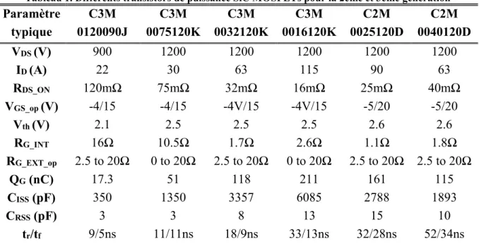
Where af, k1, K2, Ka, Kb, Kc are parameters to adjust the equation regarding to each power transistor. These parameters can be easily manipulated to get the image curve of the CGD non linearity compared to datasheet, as illustrated in Fig.I. 4. The used datasheet curve is from the Wolfspeed second generation transistor C2M0025120D, where CGD_Min= 15pF.
Fig.I. 4. Comparison curve of the "small signal" nonlinear capacitance CGD, between datasheet and eq.(I.2).
This expression is mainly based on the mathematical function, hyperbolic tangent tanh(x), which allows three operation regions: The first region is marked by the sharp decrease of the capacitor value, from CGD-Max to an approximate CGD-Min. At this region, VGS is at its maximum
P h D t h e s i s o f B a r a z i Y a z a n P a g e 21 | 225 value and VDS= 0V. The hyperbolic tangent tends towards -1, which leads to eq. (I. 6). K2 is approximately equal to ½. With VGD<VGS_Miller.
tanh(𝐾𝑏∗ |𝑉𝐺𝐷| − 𝐾𝑐) ≈ −1 ; 𝐶𝐺𝐷 =
𝑎𝑓∗ 𝐾1 [(1 + |𝑉𝐺𝐷|)]𝐾2
(I. 6) The second region, is where there is a soft decline of the capacitor value, to reach CGD-Min. The main parameters responsible of the acute slow curve are Kc and Kb.
The third region is marked this time by CGD-Min, where the capacitor is almost constant. This time the hyperbolic tangent tends towards +1, VGS is at its minimum value, and VDS is high enough not to interfere with the value of the capacitor, eq. (I. 7). With VGD>VGS_Miller.
tanh(𝐾𝑏∗ |𝑉𝐺𝐷| − 𝐾𝑐) ≈ +1 ; 𝐶𝐺𝐷 = 𝑎𝑓∗ 𝐾1
[(1 + |𝑉𝐺𝐷|) ∗ (1 + 𝐾𝑎)]𝐾2
(I. 7)
Switching mechanism analysis
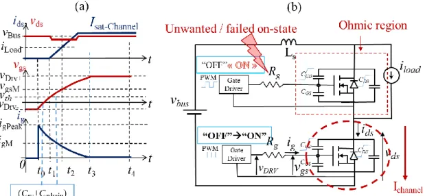
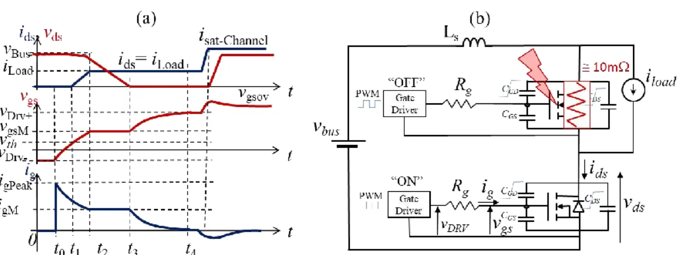
The switching characteristic was briefly introduced. In this section the switching mechanism will be developed at the turn-on and the turn-off. A commonly encountered circuit in power electronics is examined under PLECS, while simulating a power inverter leg, Fig.I.
5. Modeled SiC MOSFET are positioned on the high side HS and low side LS of the half bridge. The free-wheeling diode reverse-recovery effect is slightly taken into consideration. Parasitic inductances of the power loop and the switching loop are added as well. The load current is introduced by an ideal current source. Both MOSFETs are driven by a modeled representative gate driver which provides a command between -5/20V with a gate resistance RG= 12.5Ω with (RG_Ext + RG_int)
P h D t h e s i s o f B a r a z i Y a z a n P a g e 22 | 225 Fig.I. 6. Turn-on voltage and current waveforms of the LS MOSFET
Both transistors, HS and LS, are at the dead-time sequence where 𝑉𝐺𝑆−𝐻𝑆= 𝑉𝐺𝑆−𝐿𝑆= 𝑉𝐷𝑅𝑉− the drain current ID-LS is zero and the drain-source voltage is high 𝑉𝐷𝑆−𝐿𝑆 = 𝑉𝐵𝑢𝑠+ 𝑉𝐵𝑜𝑑𝑦_𝐻𝑆 ; with 𝑉𝐷𝑅𝑉 is the drive voltage . The turn-on waveforms of the low side are shown in Fig.I. 6, where VGS-LS rises from VDRV- (-5) to VDRV+ (+20) in four steps. At first, the gate driver provides the voltage command VDRV=VDRV+, then VGS-LS rises from VDRV- to Vth, a gate current flows through CGS and CGD-Min, the sum of this capacitors is equal to Ciss_Min. The VGS at [t0; t1] has a time-constant 𝜏 = 𝑅𝐺∗ 𝐶𝑖𝑠𝑠_𝑀𝑖𝑛. At this interval VDS-LS remains equal to 𝑉𝐵𝑢𝑠+ 𝑉𝐵𝑜𝑑𝑦_𝐻𝑆 and the drain current at its lowest value, zero. The gate current on the other hand reaches its peak current IG-Peak considering VGS=VDRV- and then starts to decrease, eq. (I. 8). Afterwards in the second step [t1; t2], VGS follows the same rise with the same 𝜏 constant, and the drain current begins to increase according to the linearized transfer curve with a 𝑑𝐼𝐷
𝑑𝑡 slope. At this sequence, VDS those slightly drop due to the free-wheeling diode and other phenomena by 2 ∗ 𝐿𝑝∗
𝑑𝑖𝐷_𝑆𝑎𝑡 𝑑𝑡 . The drain current ID follows the ID_Sat equation which is given in eq. (I.11).
𝐼𝐺_𝑃𝑒𝑎𝑘 = 𝑉𝐷𝑅𝑉+− 𝑉𝐷𝑅𝑉−
𝑅𝐺−𝐸𝑋𝑇+ 𝑅𝐺−𝑖𝑛 ; 𝐼𝐺𝑆1(𝑡) = 𝐶𝑖𝑠𝑠−𝑀𝑖𝑛 𝑑𝑉𝐺𝑆
𝑑𝑡 (I. 8)
Once the MOSFET is carrying the full load current ILoad added to the recovery current of the freewheel diode if this one is a PIN diode, ID=ILoad, the VGS becomes temporarily clamped at a plateau called the Miller plateau if Early effect is neglected, where VGS=VGS_M.At this sequence [t2; t3] the gate current is maintained in a plateau as well, due to the reverse capacitor Crss, eq.
P h D t h e s i s o f B a r a z i Y a z a n P a g e 23 | 225 (I. 9) in the equation below the Miller plateau is considered constant. This causes the drain-source to drop with 𝑑𝑉𝐷𝑆
𝑑𝑡 rate. Note that ISat is higher than ID=ILoad. 𝐼𝐺𝑆−𝑀 = 𝑉𝐷𝑅𝑉+− 𝑉𝐺𝑆−𝑀
𝑅𝐺−𝐸𝑋𝑇+ 𝑅𝐺−𝑖𝑛 (I. 9)
𝑉GS−Miller= (2 ∗ Coss∗ VDRV+) + [C𝐺𝐷 ∗ (𝐼𝐷+ 𝑔𝑓𝑠∗ 𝑉𝑡ℎ)]
2 ∗ Coss+ RG∗ C𝐺𝐷 ∗ 𝑔𝑓𝑠 (I. 10)
Eq.(I. 10) is given by finding IG-M expression and merging it with ID_M, equations below, IHS is not taken into consideration, in those equations, but added in the main one by taking into account the high side capacitance, CT is the capacitor of the depletion zone :
𝐼𝐷−𝑀 = 𝐼𝐷−𝑆𝑎𝑡 − 𝐶𝐺𝐷∗dVGD dt + C_DS ∗ dVDS dt + IHS 𝐼𝐻𝑠 = 𝐶𝑇∗𝑑|𝑉𝐺𝐷| 𝑑𝑡 (I. 11) With dVGD dt + dVDS dt = dVGS dt ; 𝑉𝐺𝑆 = 𝐶𝑡𝑒 → dVGD dt = −dVDS dt (I. 12) Therefore ID−M = ID−Sat− 𝐶𝑂𝑆𝑆∗dVGD dt + 𝐶𝑇∗ 𝑑|𝑉𝐺𝐷| 𝑑𝑡 (I. 13)
Eq. (I. 14). is giving by replacing ID_Sat by its basic equation ID−M = gfs∗ (VGS−M− Vth)−𝐶𝑜𝑠𝑠∗ dVGD dt + 𝐶𝑇∗ 𝑑|𝑉𝐺𝐷| 𝑑𝑡 (I. 14) Finally, 𝐼𝐺𝑆−𝑀 = 𝐶𝐺𝐷∗ [𝑔𝑓𝑠∗ (𝑉𝐺𝑆−𝑀− 𝑉𝑡ℎ) − 𝐼𝐷−𝑀] 𝐶𝑜𝑠𝑠+ 𝐶𝑇 (I. 15)
Above the Miller plateau was considered constant, for a non-constant Miller plateau 𝑑𝑉𝐺𝑆 𝑑𝑡 ≠ 0, the Early effect should be considered. The equation ID should be changed as well, taking into consideration the Early effect, eq.(I. 16). In the ID-VDS characteristic merit curve at the saturation region, the curve shows a positive slope due to Early effect, where UX is negative and equal to few volts.
𝑖𝐷 = 𝐾′ ∗ (𝑉𝐺𝑆− 𝑉𝑡ℎ) ∗ (1 −
𝑉𝐷𝑆− 𝑉𝐺𝑆 + 𝑉𝑡ℎ
𝑈𝑋 ) (I. 16)
In addition to these equations, one may replace VGS_M in the equation (I. 17) to express dVDS/dt. The decrease of VDS occurs in two steps. The first step corresponds to the current flow through the active region where CGD is minimal, then the second step is where the transient is in the ohmic region, and the CGD is maximal.
P h D t h e s i s o f B a r a z i Y a z a n P a g e 24 | 225 dVDS dt = 1 CGD∗ VGS−M− VDRV+ RG (I. 17) dVDS dt = − gfs∗ (VDRV+− Vth) − ID (Coss+ CT) + RG∗ CGD∗ gfs (I. 18)
In the last sequence [t3; …] the MOSFET need to maintain the entire load current. VDS completely drops to the on-state value of ID*RDS_ON. The gate-voltage resume its growth, but this time with a different time constant 𝜏 = 𝑅𝐺 ∗ 𝐶𝑖𝑠𝑠−𝑀𝑎𝑥. Finally the gate-current decreases towards zero, eq.(I. 19).
𝐼𝐺𝑆3(𝑡) = 𝐶𝑖𝑠𝑠−𝑀𝑎𝑥 𝑑𝑉𝐺𝑆
𝑑𝑡 (I. 19)
The free-wheeling diode affects the switching waveforms. The reverse recovery current is slightly introduced in the waveforms (body diode). Its cause the small decrease of VDS in the second sequence. Therefore, in the third sequence, the drain current rises above ILoad; causing VGS to increase beyond the Miller plateau. Those increase can be high, but they are present for a short period off time and decrease rapidly when the diode current snaps off and recovers to zero.
Fig.I. 7. Turn-off voltage and current waveforms of the LS MOSFET
The turn-off of the MOSFET is mostly the inverse sequence of events that occurs during the turn-on, Fig.I. 7. The same basic analytical approach used in the turn-on can be used under the
P h D t h e s i s o f B a r a z i Y a z a n P a g e 25 | 225 turn-off waveforms. The value of RG used during turn-off may be different from that used during the turn-on.
The turn-off sequence can be cut into four sequences, basically tracking the turn-on steps. The sequences are assured by, the gate-source voltage VGS drops from VDRV+ to VDRV- inversely following the turn-on sequence. VDS goes back to its high value VBus, causing the transistor to open. Some of the capacitors are gradually discharged and others charged [18] [19] [20].
The electrical switching results in power losses, which can be divided into two categories. The gate driver losses of the device and the transistors switching losses. As presented in Fig.I.
6 and Fig.I. 7, the total gate charge QG describes the transfer charge amount while the voltage across the input capacitance changes. Therefore, the VGS-QG typical curve characteristic generates the total gate charge. Thus the gate charge losses is given eq.(I. 20), where fDrv is the switching frequency:
𝑃𝐺𝑎𝑡𝑒 = 𝑉𝐷𝑟𝑣∗ 𝑄𝐺|𝑉𝐷𝑆_𝑀𝑎𝑥∗ 𝑓𝐷𝑟𝑣 (I. 20)
On the other hand, the switching losses occurs due to high current and high voltage being present in the device simultaneously for a short period. In order to ensure the least amount of switching losses, the duration of this time interval must be minimized. The only interval time where it is possible; it is the interval time that corresponds to the linear (ohmic) operation of the device. It is when the gate voltage is between Vth and VGS_M, causing changes in the current of the device and to the Miller plateau region when the drain voltage goes through its switching transition. Even though the switching transitions are well understood, calculating the exact switching losses is almost impossible. The reason is the impact of the parasitic inductances and capacitances.
The behavior and length of both turn-on and turn-off sequences are a function of the parasitic capacitances values, the parasitic inductance values, the required voltage change across these capacitors, the gate internal/external resistance and the available gate driver current.All this brings into play the importance of the proper component as presented above, and the efficient gate drive design. All of this behavioral study helped us to well identify normal on behavior, which is a key to distinguish between short-circuit behavior and normal turn-on. The short-circuit can be detectible by two means, rather by detecting the short-circuit behavior or by detecting the absence of Normal Turn On NTO. Moreover, the detection circuit should not at any point detect normal behavior.
Gate Drivers for SiC FETs
This section proposes to demonstrate a systematic approach to design high performance gate drive circuits for high speed switching applications. In order to keep up with the WBG growth, the performances of the gate driver should involve and should face the common design challenges. The main gate driver features are high efficiency, advanced protection and compact solution. With WBG power FETs such as SiC MOSFETs, the gate drivers should also adapt to
P h D t h e s i s o f B a r a z i Y a z a n P a g e 26 | 225 their specificities (e.g. gate charge, capacitance values, threshold voltages, voltage range and maximum ratings, high switching speeds, …)
Gate Drivers fundamentals for power FETs
The primary function of a gate driver circuit is to switch a power semiconductor device from the off state to the on state and vice versa. MOSFET transistors are mainly driven by the high and low voltage between the VGS [21]. There are mainly two types of control, voltage control and current control. Current control is a technique based on a full H-bridge and an inductive element that reduces control losses by recovering part of the energy used to control the gate of a power transistor. This type of control is very complex for small gains in the order of a watt when using converters with a power of few kilowatt range, and very usfl at high switching frequencies [22] [23].
Gate driver functions
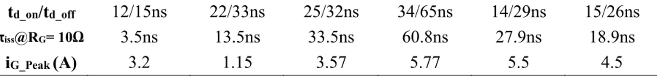
The basic topology of the gate driver circuit consists of three fundament block functions. First, the amplification circuit (buffer and pre-amplification), which provides the gate current and voltages to charge and discharge the input capacitor of the power transistor. The second functionality is the dc gate driver power supply. And last is the isolation. The signal processing and external control circuit that generate the logic level controls signals (FPGA, µprocessor, etc), which probably needs electrical isolation as well, Fig.I. 8. On the other hand, primary logic circuit is included within the gate driver. Additional functionalities are added with time, to complete the basic gate driver, in different many levels:
Switching and I/O transmission monitoring
Health monitoring
Safety monitoring (device and auxiliary voltage supply)
Those functionalities push a large part of the control circuit to merge with the drive circuit. Nowadays, the basic gate driver consists of a variety of function responding to the challenges the WBG devices bring along with their growth. All of this while keeping the low cost and minimization of the gate drivers circuit in mind.
In order to drive the power semiconductors properly, they are few considerations that need to take place. The first consideration is to drive the switch and with low switching losses and acceptable EMI/EMC specifications. Which leads us to the first function on the gate driver, the amplification circuit or the output buffer which provides the source/sink current towards the power transistor’s gate and source electrodes. The second function on the gate driver, the gate driver power supply, its main function is to provide the gate voltages relatively to the source or Kelvin source electrode. As maintaining the switch in ON state and to make sure that the voltage drop is minimum which corresponds on reducing the conduction losses. As well as maintaining safely the switch in OFF state, in order to minimize the drain-source leakage current and prevent accidental turn-on. Last and not least, one of the important consideration is the noise immunity, in order to tolerate large static and dynamic ground-potential differences and disruptive ground
P h D t h e s i s o f B a r a z i Y a z a n P a g e 27 | 225 loops in circuit that have high energy. Which brings the importance of the last function, the isolation, separate the power ground and the signal ground.
Different gate driver architectures are proposed in the literature adapted to SiC applications, each focused in a different function and with different configurations, in order to have better figure of merits [24] [25] [26] .
Fig.I. 8. Block diagram of a synchronous buck converter presenting the essential gate driver functions for the control of both HS and LS (ADuM4121 isolated gate drivers)
Tab.I. 1. Driver Configuration overview, Infineon [27]
Types Definition
Single-channel low-side driver
Allows low offset of the voltage between input and
output Single-channel
high-side driver
Allows high voltage offset between input and output
Dual-channel low-side driver
Both channels allow individual low voltage
offsets, no interlock
Dual-channel high-side driver
Both channels allow individual high voltage
P h D t h e s i s o f B a r a z i Y a z a n P a g e 28 | 225 High and low-side
driver
Two non-interlocked channels, one for high, one
for low voltage offsets
Half-bridge driver
Two interlocked channels where one of the channel allows a high voltage offset
Full-bridge driver
Four channels in a package with two independent half
bridges
Three-phase bridge
Six channels in a package with three independent half
bridges
Gate driver fundamental parameters
There are five main important gate driver parameters, which have a big impact on the system. The first one is the negative voltage handling. The negative voltage handling is the ability of the gate driver to withstand negative voltages at the input and output. This negative voltage spikes can result from parasitic inductances from switching transition, leakage or even the poor layout design. The second one is the gate drive source/sink currents, which allows to charge and discharge the gate capacitance power switch. The higher the drive current capability, the faster the capacitance can be charged or discharged. Therefore, being able to turn-on/off a MOSFET quickly, can help to minimize the power switching losses, albeit with higher impacts on EMI (Electro-Magnetic Interference) and EMC (Electro-Magnetic Compatibility) issues. Which leads to the gate driver to source/sink large amount of current. The third one is the delay matching and dead-time management. Dead-time is the period during which neither devices is switched to avoid any potential overlap when they are in half-bridge configuration. As the switching is faster, the dead times are smaller. The management of the dead time between HS and LS is critical, and therefore the classical dispersions on the propagation times between HS and LS can be problematic. Delay matching is where the internal propagation delays between
P h D t h e s i s o f B a r a z i Y a z a n P a g e 29 | 225 the channels are matched. The smaller the delays specification, the better performing the gate driver. During the dead time, current flows back through the IGBT or MOSFET body diode, as shown in Fig.I. 9. The body diode has a much larger voltage drop than the device itself, and thus there are more conduction losses. The longer the dead time, the higher the losses, which reduce efficiency and generate heat. Thus, it is best to minimize the dead time by using a gate driver with low pulse-width distortion, low propagation delay, and small rise and fall times. The delay matching and dead-time management provide several benefits. As the paralleled MOSFETs are driven in simultaneous fashion with minimum turn-on delay difference. Other benefit is, it eases paralleling of gate driver output to effectively double current capability and to ease driving parallel power switches. Additionally, rise and fall time may also affect the overlap of these signals, Fig.I. 9. The fourth parameter is VDrv+ the positive supply voltage, and VDrv- the negative one, which define the operational range of drive outputs. The fifth one is the operating temperature range, which robustness should be satisfied under extreme temperatures.[28]
Fig.I. 9. (a) Synchronously switched half bridge (b). Pulse width distortion (c). Effect of propagation time [29]
Isolation
The isolation in the gate driver is the electrical separation between various functional circuits such that there is no direct conduction path available between them, Fig.I. 10. This allows individual functions to possess different reference potentials. Signal and/or power can still pass through isolated functions using inductive, capacitive, or optical paths. The isolation can be located in different spots:
Between the primary logic control (microprocessor / FPGA) and the secondary control (Connected directly to the gate driver).
Between the power supply of each side, high side and low side.
Between the low side gate driver and the high side gate driver.
P h D t h e s i s o f B a r a z i Y a z a n P a g e 30 | 225 Gate drivers can be classified in two main categories with respect to isolation. Non-isolated gate driver, and isolated gate drivers.
Non-isolated technology refers to gate driver ICs utilizing low voltage circuitry, most of them are low-side gate drivers. In other words, the input signal levels of conventional low-side gate driver ICs are referenced to the ground potential of the gate driver IC. For high-side non isolated gate drivers, the direct drive can be generated by a level shifted drive and bootstrap technique. The level shifter is a circuit used to shift the voltage domain. There are 600V level-shifters which transfer the signals to the fully insulated high sides, where the differential transmission signals are filtered and reconstructed. The bootstrap power supply is one of the most common techniques for suppling power to the high-side driver circuitry due to its simplicity and low cost. The bootstrap power supply mainly consists of a bootstrap diode or an active synchronous-diode and capacitor.
The presence of high voltage functions can introduce significant potential differences, which may cause damaging DC currents or unwanted AC currents to flow to other parts of the system of the gate driver. This may cause errors or create hazardous conditions of operation. In these circumstances galvanic isolation is needed. The galvanic isolation is not only used to separate the high voltage side from the low voltage side but they are used for human safety and are mandatory by standards; prevent ground potential differences, or ground loops and improve noise immunity as well. There are multiple topology options available to isolate the gate driver functions,[30] .
Fig.I. 10. Two Different level topology of isolation, according to IEC 60664-1 and IEC 61800-5-1
There are three primary technologies used for analog and digital isolation of signals today-- optical, inductive, and capacitive, Fig.I. 11. Each technology uses a different insulator material with different dielectric strength. Dielectric strength is a measurement used to describe the maximum applied electric field that a material can withstand without undergoing electrical breakdown and becoming electrically conductive. As for Air the dielectric strength is 1Vrms/µm, for Polyimide it is 300Vrms/µm and for SiO2 it is 500Vrms/µm, which depends on the conditions of distance, pressure and humidity in particular, etc.
An optical isolator or opto-coupler consists of an input LED, a receiving photodetector, and an output driver. The driver circuit and LED circuits are typically built using
P h D t h e s i s o f B a r a z i Y a z a n P a g e 31 | 225 Complementary Metal Oxide Semiconductor technology, or CMOS technology. Both the input and output of the opto-coupler require a separate voltage supply connected through an anode and collector pins and separate grounds, typically connected through a cathode or emitter pin, in order to maintain signal isolation between input and output. The opto-coupler isolation has high power consumption. An electrostatic shield layer can be also embedded to reduce the common-mode capacitive coupling between inputs (signal and ref.) and outputs (signal and ref.).
Inductive isolators are based on a magnetic transformer technology or core-less magnetic transmission on silicone / Al2O3 substrate. The logic inputs are used to generate an electromagnetic field and to transfer proportional energy signals across the inductive transformer barrier.
Differential capacitive isolation is based on energy transfer across the silicon dioxide, or CMOS barrier, through a high frequency carrier. A digital input signal is applied and modulated, then communicated across the isolation barrier. A proportional output is then produced to the level of the measured signal at the input. Because capacitive isolators are designed with the highest dielectric strength material for insulation, they offer high data rates, low thermal profiles, and long lifetime operation. The method does not need a power supply and has less power consumption compared to the opto-coupler.
Fig.I. 11. Different isolation technologies [29]
Isolated gate drivers can have different galvanic isolation integrated in different places, depending on its functionality [27]:
Basic isolation: Certified isolation applied to live parts to provide basic protection against electric shock.
Functional isolation: Isolation between conductive parts only for the purpose of correct equipment operation.
Supplementary isolation: Additional isolation to basic isolation as a fallback solution in case basic isolation fails.
Double galvanic isolation: Certified isolation consisting of both basic isolation and supplementary isolation.
Reinforced Isolation: single certified isolation applied to live to protect against electric shock.
P h D t h e s i s o f B a r a z i Y a z a n P a g e 32 | 225
Buffer Architecture
There are different topologies for the output buffer. It depends on different parameters such as the sink/source current, the gate resistor, the type of the used transistors, the voltage levels, … The most common architectures are presented in this section. Fig.I. 12. presents different inverter structures. The Totem-pole and the push-pull variants structures are the elementary architectures of the output buffer. The inverter of totem pole consists of two identical switches of the same type in serial. The switches can be two NMOSs or two NPNs, which requires two complementary command signals (Com1 and Com2) delayed with a small dead time, Fig.I. 12 (b). On the other hand, the push-pull inverter consists of two opposite switches in series (NMOS + PMOS or NPN+PNP), Fig.I. 12 (c). [18]
Fig.I. 12. Three elementary output buffer structures with a single gate resistance.
These structures are named non-differential 2-level buffers and require two power supplies or with the possibility of having the lower one two the ground, which makes it only one gate power supply. The command signal requires a generation of an internal dead time for the buffer, driving one power transistor. Moreover, the structures are presented with one resistance. Nevertheless, it is interesting to dissociate the gate resistance into two elements, where each resistance is in series with a switch (HS and LS), Fig.I. 13.(b). In addition to dissociation the turn-on resistance RG_ON from the turn-off resistance RG_OFF, the absence of internal dead time in the driver is allowed. The short-circuit current is limited by the presence of the two resistors. In a Push-Pull configuration, are complementary, this allows the use of only one control signal,
P h D t h e s i s o f B a r a z i Y a z a n P a g e 33 | 225 Fig.I. 13.(b), also known as split output buffer. The separation of this commands signals allows more flexibility on the dead time behavior, Fig.I. 13.(c), and easy settings of different gate resistors for turn-on and turn-off.
Fig.I. 13.(d) presents a different structure with separate gate resistances for the PMOS and NMOS, which allows more flexibility to control the gate current [31], also known as segmented buffer. Several slew rate control methods have been designed to adapt the charging/discharging speed of Ciss. The capacitor charging/discharging speed is affected by four aspects, which are: gate driver voltage, gate resistance, gate current, and Ciss. Consequently, the AGD (active gate driver) methods can be divided into four different methods: variable gate resistance method, variable input capacitance method, variable gate voltage method, and variable gate current method. These methods will be further developed in the section below.
Fig.I. 13. Four elementary output buffer structures with a several gate resistances.
The illustrated structures offer only two output voltage levels, VDC1 and VDC2, in other words VDrv+ and VDrv-. Fig.I. 14 presents different named differential 3-level architectures, with the flexibility to change the output voltage levels and therefore the gate to source voltage levels of the power transistor. Fig.I. 14 (a) and (b) presents the H-bridge structure, the benefit from this structure is the possibility to have three or even four output voltage levels, VDrv+,0,VDRV-, and another intermediate level. With these structures the split gate resistance or the split command is mandatory. These structure applies a different voltage level at the gate and the source of the power transistor with only a reduced number of power supply. Fig.I. 14 (c) presents a last structure with two output voltage levels VDrv+ and VDrv-, but in this structure the commands of
P h D t h e s i s o f B a r a z i Y a z a n P a g e 34 | 225 each side is supplied with different power supplies. In other words, structures in Fig.I. 14 (a) and (b) are limited at the power supply voltage, if the gate oxide of the PMOS and NMOS does not support the same power supply voltage. As an example if VDC2 in (a) and (b) is equal to 20V the VGS-PMOS of the PMOS should support the 20V. Therefore, Fig.I. 14 (c) is an alternative to use the split power supply (VDC1, VDC2, VDC3, VDC4)which allows the use of transistors with less gate breakdown voltage.
Fig.I. 14. Three elementary output buffers structures with split gate resistance, and split power supply.
SiC MOSFET power device and the challenges faced by the gate
driver
The emerging of SiC MOSFET is an attractive replacement of Si IGBT for high voltage and high power density applications. Due to the similar MOS gate structure, the gate drivers for SiC MOSFETs can directly inherit from the Si IGBTs various functions. However, the high switching speed with increasing dv/dt and di/dt ratios makes the gate driver design for SiC MOSFET new challenges. The high dv/dt and di/dt may lead to parasitic effects including phase-leg crosstalk and Electro-Magnetic Interference (EMI) issues due to the ringing. Therefore, the gate driver design for SiC MOSFETs should follow such features:
Negative gate driver power supply to avoid crosstalk in half-bridge configuration;
A low impedance path for faster turn-off and suppression of crosstalk;
A small gate loop inductance to reduce the gate-source voltage ringing, especially the common source inductance should be minimized to reduce the interference between the two loops;
P h D t h e s i s o f B a r a z i Y a z a n P a g e 35 | 225
A small power loop inductance to reduce the ringing of drain-source voltage and drain current with the low-ESL (equivalent stray inductance) decoupling capacitance placed as close as possible.
High gate source/sink current for fast switching
Moreover, the short-circuit SC withstanding time for SiC MOSFETs is shorter then Si IGBTs. Short-circuit faults are the most critical failure mechanism in power converters, which may result from the controller fault, device failure breakdown, or load short-circuit. Due to the excessive power dissipation during the short-circuit transient, the device junction temperature may easily exceed the limit and lead to thermal runaway and fail-to-short permanent failure, sometimes explosion. The device manufacturers normally specify a short-circuit withstand capability, which is the amount of time from the start of short-circuit fault until the device exhibits a sign of irreversible damage.
Fig.I. 15. Principle topology of monitoring [32]
In order to maximize switching performance with lower switching losses, the drivability should be enhanced. The work of this thesis is focused on monitoring oriented safety and oriented switching and transmission. Several buffer structures can be proposed to further enhance and overcome the challenges faced by the SiC MOSFETs [33], or GaN power devices [34]. Moreover, different functions can be added in the gate driver. These functions and structures can be classified in three categories, switching and transmission monitoring, safety monitoring and healthy monitoring. These monitoring includes:
Dead-time management and switching time monitoring [7],
Voltage control and measurement (dVDS/dt, VDS) [36], overvoltage protection,
Current control and measurement (dID/dt, ID) [37], overcurrent protection [3], peak gate current measurement,
![Figure 1. Évolution et Domaines d’applications ; des semi-conducteurs discrets de puissance [1]](https://thumb-eu.123doks.com/thumbv2/123doknet/2943812.79417/181.892.170.734.655.982/figure-évolution-domaines-applications-semi-conducteurs-discrets-puissance.webp)