HAL Id: hal-00554779
https://hal-iogs.archives-ouvertes.fr/hal-00554779
Submitted on 27 Feb 2012
HAL is a multi-disciplinary open access
archive for the deposit and dissemination of
sci-entific research documents, whether they are
pub-lished or not. The documents may come from
teaching and research institutions in France or
abroad, or from public or private research centers.
L’archive ouverte pluridisciplinaire HAL, est
destinée au dépôt et à la diffusion de documents
scientifiques de niveau recherche, publiés ou non,
émanant des établissements d’enseignement et de
recherche français ou étrangers, des laboratoires
publics ou privés.
Bragg diffraction in thin 2D refractive index modulated
semiconductor samples
Qiong He, Isabelle Zaquine, Gérald Roosen, Robert Frey
To cite this version:
Qiong He, Isabelle Zaquine, Gérald Roosen, Robert Frey. Bragg diffraction in thin 2D refractive index
modulated semiconductor samples. Journal of the Optical Society of America B, Optical Society of
America, 2009, 26 (3), pp.390-396. �hal-00554779�
Bragg diffraction in thin 2D refractive index
modulated semiconductor samples
Qiong He,1,2Isabelle Zaquine,1,*Gerald Roosen,2and Robert Frey1,2
1
Institut TELECOM/Télécom ParisTech, Laboratoire de Traitement et de Communication de l’Information, CNRS, 46 rue Barrault, 75634 Paris cedex 13, France
2
Laboratoire Charles Fabry de l’Institut d’Optique, Institut d’Optique Graduate School, CNRS et Université Paris Sud, Centre Scientifique Paris Sud, Bât 503, 91403 Orsay cedex, France
*Corresponding author: [email protected]
Received October 17, 2008; accepted December 8, 2008; posted December 18, 2008 (Doc. ID 102927); published February 4, 2009
A very simple model has been developed to describe the diffractive properties of a crossed grating structure of the refractive index formed by a thin transmission grating recorded in a Bragg reflector. When the Bragg con-dition of the transmission grating coincides with the band edge of the reflection grating seen as a one-dimensional photonic crystal, the diffraction efficiency and wavelength selectivity of the transmission grating are highly enhanced and a Bragg diffraction regime can be obtained, even in very thin samples. The model can be used to design micrometric very efficient new diffracting devices for optical signal processing. © 2009 Op-tical Society of America
OCIS codes: 050.1950, 190.2055, 230.1480.
1. INTRODUCTION
Transmission gratings are widely used for optical signal processing [1]. Their performances are nevertheless lim-ited by the small refractive index modulation that can be obtained in usual nonlinear materials. The thickness is also an issue as it must not be too large if an integrated device is wanted, although the diffraction regime associ-ated with thin crystals is a Raman–Nath regime involv-ing multiple diffracted beams. Besides the already well-known simple [2–4] and double resonance [5–9] in a Fabry–Perot cavity, a new approach using slow light at the band edge of a one-dimensional photonic crystal (1D-PC) was recently demonstrated to overcome these difficul-ties, first in photopolymers [10] and then in semiconduc-tor Bragg reflecsemiconduc-tors [11]. Results are especially attractive in the latter case due to the high index contrast of Bragg reflectors. The investigations concern the efficiency, wave-length selectivity, and diffraction regime of thin low index modulation transmission gratings when they are recorded in a reflection grating and form a two-dimensional (2D) structure of the refractive index. Huge performance im-provements can be obtained when the read beam wave-length and incidence angle correspond to the band-edge resonance of the reflection grating seen as a 1D-PC and satisfy the transmission grating Bragg condition. In this paper, a very simple analytical four-wave model is pre-sented in order to predict the diffraction properties of a 2D refractive index modulated structure and to enable the design of optimized devices for various applications.
The crossed grating device considered in this paper is described in Section 2. The analytical model used to study its diffraction properties is developed in Section 3. Perfor-mance enhancement predicted by the model for samples exhibiting a high refractive index step modulation of the reflection grating as seen in semiconductor Bragg mirrors
for instance are presented in Section 4 as well as the most favorable case of samples, where the 2D grating is depos-ited on a mirror that combines the reflected and the transmitted diffracted beams into a single reflected dif-fracted beam. Finally, the influence of various parameters on the diffractive properties of such samples is detailed.
2. CONSIDERED STRUCTURES AND
WAVES
The crossed grating structure has periodicities⌳xand⌳z
in the x and z directions, respectively (see Fig.1). The in-cident beam lies in the xz plane with a small incidence angle R
⬘
with respect to the z axis. The grating with fringes parallel to the z direction diffracts in the so-called transmission mode while that recorded with fringes par-allel to x operates in the so-called reflection mode [12]. The periodic dielectric permittivity 共z,x兲 satisfies the equation共z + pz⌳z,x + px⌳x兲 = 共z,x兲, 共1兲
where pzand pxare positive or negative integers. For the
reflection grating, the Bragg condition (maximum reflec-tion) is satisfied at0 for this incidence angle. However, our aim is not maximum reflection as we wish to maxi-mize the local field [13–17] to enhance the diffraction ef-ficiency of the transmission grating. That is why the 2D periodic structure is designed to operate at the upper band edge of the 1D-PC, herein the reflection grating 共BE⬎0兲, when the read beam incidence angle R
⬘
andwavelength BE satisfy the transmission grating Bragg condition 共BE= 2⌳xsinR
⬘
兲. It should be pointed out thatthe Bragg condition in thick transmission gratings usu-ally ensures maximum diffraction efficiency, whereas here in the case of thin samples, it merely means that the
−1 order diffraction angle on the transmission grating is opposite to the incidence angle. In this way, both read and diffracted beams can be enhanced through the band-edge resonance of the reflection grating. This enhancement, giving rise to a single diffracted beam, is possible only if the initial diffraction efficiency of the transmission grat-ing is low. Therefore, we only consider nanostructured materials exhibiting a small refractive index modulation in the x direction. The dielectric permittivity can then be written as
共z,x兲 = 共z兲关1 +z共x兲兴, 共2兲
where共z兲 andz共x兲 are periodic in the z and x directions,
respectively, (共z+pz⌳z兲=共z兲 and z共x+px⌳x兲=z共x兲Ⰶ1).
Concerning the reflection grating having its wave vector Kz= 2/⌳zin the z direction, we are interested in high
in-dex modulation step gratings as in multilayered Bragg mirrors. The z dependence of the dielectric permittivity given in Eq.(2)is then
共z兲 = 1for pz⌳z艋 z ⬍ pz⌳z+ e1,
共z兲 = 2for pz⌳z+ e1艋 z ⬍ 共pz+ 1兲⌳z, 共3兲
where e1is the thickness of the layer of dielectric permit-tivity1.
For the low modulation refractive index grating along the x direction, z共x兲 can then be replaced by the first
term of its Fourier expansion (an even function is consid-ered here for the sake of simplicity without any loss of generality)
z共x兲 = mx1cos共Kxx兲 for pz⌳z艋 z ⬍ pz⌳z+ e1, z共x兲 = mx2cos共Kxx兲 for pz⌳z+ e1艋 z ⬍ 共pz+ 1兲⌳z,
共4兲 where Kx= 2/⌳xis the wave vector of the transmission
grating and mxi共i=1,2兲 is the permittivity modulation of
the transmission grating in the medium of refractive in-dex ni=
冑
i.3. MODEL
A. DescriptionRather than use a “rigorous coupled waves” method [18–21], where a large number of diffraction orders is taken into account involving large computation times and stability issues, the modeling of this multilayered me-dium consists of describing the layers separately (Fig.2). Each dielectric layer is separated from its neighboring layers by two interfaces where reflection takes place be-cause of the dielectric permittivity discontinuity. More-over, inside each layer, the recorded transmission grating gives rise to diffraction. Our analytical approach of beam propagation (including diffraction on the transmission grating) is based on the nonlinear optics formalism, where only the terms close to phase-matching are kept in the propagation equation. We have then chosen to evalu-ate how many diffraction orders can reasonably be non-negligible in the considered structure. As demonstrated hereinafter, the diffraction of an incident read wave EIon the crossed gratings structure considered in our study mainly involves four waves in the nonlinear medium (Fig.
2). As the medium with a periodically modulated suscep-tibility can be considered as infinite in the x axis direc-tion, perfect phase-matching is always achieved in this di-rection, which determines the direction of the various waves (Fig.3).
ERFiis the forward propagating read wave in the me-dium of refractive index ni. Only TE polarization has been
investigated in this paper but TM polarization would not make much difference considering the small incidence angles used. For the reflection grating with a wave vector
Kz the phase-matching condition gives rise to a single backward propagating diffraction order ERBi (reflected beam) in which the direction is determined by the Des-cartes laws at the interfaces between adjacent layers.
Forward and backward diffracted waves ESFiand ESBi with wave vectors kSFiand kSBioriginate from the −1 dif-fraction order of ERFiand ERBi with wave vectors kRFi and kRBion the transmission grating of wave vector Kx,
Fig. 1. (Color online) Two-dimensional refractive index modu-lated structure. In the x direction, the modulation is sinusoidal with a period⌳x, and in the z direction it is a step modulation
made of N pairs of quarter-wave layers of respective indices n1
and n2, with a period⌳z. EI, ER, ET, EDTand EDR are, respec-tively, the incident, reflected, transmitted, diffracted transmit-ted, and diffracted reflected waves.
Fig. 2. (Color online) Four main waves taken into account in the crossed gratings structure are shown in one quarter-wave layer with an index n2and a thickness e2=⌳z− e1. Each wave is
repre-sented by the direction of its wave vector. The matrix D2
de-scribes the diffraction in the layer and the matrices R12and R21
and the diffraction properties of the device can be accu-rately described by using only these four waves as will be justified later by computing the intensity of the strongest phase mismatched diffraction order, the +1 order.
If the read wave incidence on the transmission grating with respect to the z axis isRi共nisinRi= sinR
⬘
兲 in themedium with a refractive index ni, and the read
wave-length BE, then the direction D−1i of the −1 order
dif-fracted wave in the same medium is given by the phase-matching condition in the x direction (Fig.3)
D−1i= Arcsin关− BE/共ni⌳x兲 + sin共Ri兲兴. 共5兲
At Bragg incidence on the transmission grating共sin共Ri兲 =BE/共2ni⌳x兲兲 the symmetry between the read and −1
dif-fraction order waves共D−1i= −Ri兲 provides them with the
same band-edge enhancement.
The propagation direction of the +1 diffraction order is D+1i= Arcsin关BE/共ni⌳x兲 + sin共Ri兲兴. 共6兲 Therefore, it does not benefit from the local field enhance-ment of the 1D-PC band edge. The very simple four-wave model that is detailed hereinafter can be used either to calculate the −1 diffraction order or the +1 diffraction or-der, provided the right diffraction angles are taken into account. The depletion of the read beam by the −1 diffrac-tion order is not taken into account when computing the +1 order, which leads to an overestimation of the inten-sity of this higher diffraction order. It will be nevertheless demonstrated that its intensity is very small compared to that of the main diffraction order and that the Bragg dif-fraction regime can be easily obtained in most situations.
B. Matrix Resolution
In our analysis, the diffraction properties of the 2D device are naturally described using a matrix formalism. A four-dimensional (4D) vector is formed in each layer with the complex amplitudes of the read wave, the reflected wave, the diffracted wave, and the reflected diffracted (or dif-fracted reflected) wave so that reflection on an interface and diffraction on the transmission grating in one layer can be represented by 4⫻4 matrices.
At every interface between adjacent layers, the reflec-tion matrix is deduced from the boundary equareflec-tions [22]
冢
ERFi ERBi ESFi ESBi冣
= Rij冢
ERFj ERBj ESFj ESBj冣
= 1 tij冢
1 rij 0 0 rij 1 0 0 0 0 1 rij 0 0 rij 1冣
冢
ERFj ERBj ESFj ESBj冣
, 共7兲where rij=共nicosi− njcosj兲/共nicosi+ njcosj兲 and tij
= 2nicosi/共nicosi+ njcosj兲; ni andiare, respectively,
the refractive index and propagation angle of the forward propagating wave in the layer number i.
To calculate the diffraction matrix, we use the reso-lution of the coupled wave equations for the forward read and diffracted waves and for the backward read and dif-fracted waves:
冦
RFi z + ki⬙ cosRiRFi= i⌬ni cosRiSFi SFi z +冉
ki⬙ cosRi− i⌬ki冊
RFi= i⌬ni cosDiRFi冧
共8a兲冦
−RBi z + ki⬙ cosRiRBi= i⌬ni cosR SB −SBi z +冉
ki⬙ cosRi− i⌬ki冊
SBi= i⌬ni cosDiRBi,冧
共8b兲 where再
ERFi,RBi共z兲 = RFi,Bi共z兲exp共±ikRFi,RBicosRiz兲ESFi,SBi共z兲 = SFi,Bi共z兲exp共±ikSFi,SBicosDiz兲
冎
, 共9兲where⌬ni= nimx/ 2 is the refractive index modulation
am-plitude in a layer of mean refractive index ni, ki= 2ni/
is the common modulus of all wave vectors at wavelength , ⌬ki=兩kSFi− kRFi+ Kx兩 is the wave vector mismatch as-sociated to the detuning from Bragg resonance on the transmission grating, and the possible loss has been in-troduced as the imaginary part ki
⬙
= 2ni⬙
/ of the wave vector.These two systems of coupled equations can be ex-pressed in a matrix form
Si共z兲
z = AiSi共z兲, 共10兲
where Si共z兲=关RFi共z兲,RBi共z兲,SFi共z兲,SBi共z兲兴
⬘
is a columnma-trix and solved by diagonalizing the mama-trix Ai, Qi
= Pi−1AiPi, where Pi is the base change matrix and Qi is
diagonal. The solutions are in the form
kz
Kx
θ
kz
Kx
x
θ
θ
z
∆
∆
k
SFk
D−1 R D+1 +1 −1k
RF SBk
RBFig. 3. (Color online) Phase-matching conditions for the four main waves in the photonic crystal when the read beam is not at Bragg incidence. The +1 diffraction order is also represented ex-hibiting a much larger phase mismatch than the −1 order. The “i” subscript referring to the considered layer type共i=1,2兲 has been omitted.
Si共z兲 = PiCiXi共z兲, 共11兲
where Xi is a 4⫻4 diagonal matrix (xj共i兲共z兲=exp共qj共i兲z兲 for
j = 1 , 2 , 3 , 4), and Ci=关c1共i兲, c2共i兲, c3共i兲, c4共i兲兴
⬘
is a column matrix of integration constants.The fields Ei共z兲=关ERFi, ERBi, ESFi, ESBi兴
⬘
= Mi共z兲Si共z兲 canthen be calculated using the diagonal matrix Mi (m1共i兲共z兲 = 1 / m2共i兲共z兲=exp共ikRFicosRiz兲 and m3共i兲共z兲=1/m4共i兲共z兲 = exp共ikRFicosDiz兲). The four integration constants of the matrix Ci are then suppressed so that the field
ampli-tudes of the four involved waves at one boundary of the considered layer i can be related to the field amplitudes at the other boundary in a matrix form:
冢
ERFi共z = 0兲 ERBi共z = 0兲 ESFi共z = 0兲 ESBi共z = 0兲冣
= Di冢
ERFi共z = li兲 ERBi共z = li兲 ESFi共z = li兲 ESBi共z = li兲冣
. 共12兲The multilayer device can then be modeled by a matrix product,
冢
EI ER 0 EDR冣
= R01D1关R12D2R21D1兴N−1R12D2R2S冢
ET 0 EDT 0冣
= F冢
ET 0 EDT 0冣
, 共13兲where each layer pair is modeled by the product R12D2R21D1 and the input output interfaces matrices have to take into account the indices of the external me-dia, either air or a semiconductor substrate.
Using this matrix product, the reflectivity 兩ER/ EI兩2,
transmission 兩ET/ EI兩2, and diffraction efficiencies T
=兩EDT/ EI兩2andR=兩EDR/ EI兩2 can be computed. The local
value of the field amplitude in the multilayered medium can also be calculated. The first higher order diffraction efficiency can be estimated in the same way and com-pared to the main diffraction order.
4. RESULTS
To obtain a significant band-edge effect, semiconductor quarter-wave layers as they are used in Bragg reflectors have been considered. GaAlAs/ AlAs [23] (n1= 3.184 and n2= 2.912) gives a permittivity modulation along the z axis mz= 11%, GaAlAs/Alox [24] gives mz= 82%, and the
highest permittivity modulation considered here is mz
= 125% with GaAlAs/air.
A. Reflection and Diffraction Spectra
As all structures exhibit the same general behavior, we have picked up as a typical case the GaAlAs/Alox struc-ture with the intermediate value of mz. Figures4(a)and
4(b)show the reflectivity and the diffraction spectra of the crossed grating structure. The center wavelength 共0 = 1170 nm兲 of the reflection grating has been chosen so
that the upper band-edge wavelength is 1.5m for tele-com applications. The sample is made of 20 layer pairs, and the period of the reflection grating is 274.5 nm. The permittivity modulation of the transmission grating is 3.10−3and its period is 8600 nm. The −1 diffraction order gives rise to a transmitted part and a reflected part, that are almost equal, which reduces the diffraction efficiency by a factor of 2. A sharp maximum can be observed at the band-edge wavelength (diffraction efficiency of 16%); the gain in diffraction efficiency is larger than 470 when com-pared to the same grating if it was recorded in a homoge-neous medium, giving clear evidence of the potentiality of the technique. The full width at half-maximum (FWHM) of this resonance is 1.9 nm, a very high wavelength selec-tivity for a transmission grating. The +1 diffraction order has also been plotted in Fig.4(b), and the corresponding efficiency is smaller than the −1 order by a factor of 20, which confirms that the +1 diffraction order does not ben-efit from the band-edge resonance and that a Bragg dif-fraction regime can be approached despite the small thickness of the device.
To increase the diffraction efficiency, a 100% reflecting mirror can be added at the back of the sample so that all the diffracted intensity can be concentrated in a single
re-Fig. 4. (Color online) (a) Reflectivity of the 1D-PC. The two semiconductors used are AlGaAs and Alox; there are 20 layer pairs, the thickness is 5.5m, the reflection grating period is 274.5 nm, and the band center wavelength is 1.17m. (b) Dif-fraction orders −1 and +1 spectra for the crossed grating device. The two considered diffraction orders give rise to a transmitted beam “DT” and a reflected beam “DR,” and the transmission grating period is 8.6m; the permittivity modulation along x is 3.10−3.
flected diffracted beam. Figure5shows that 100% diffrac-tion efficiency can be obtained in that case, even with a thinner crossed grating device (only 18 layer pairs) than in Fig.4. The FWHM is down to 1.6 nm and the diffrac-tion efficiency ratio of the main order to the higher order is 32, showing that all diffraction properties are im-proved.
B. Influence of the Structural Parameters
The next step is to calculate the effect of various param-eters of the crossed grating structure on the diffractive
properties. The maximum diffraction efficiency deter-mines the insertion loss of the device, the width of the resonance at half-maximum (FWHM) gives the wave-length selectivity, and the diffraction efficiency ratio of −1 order to +1 order R =D−1/D+1reflects the diffraction
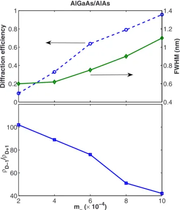
re-gime of the device. For the transmission grating, index modulation and thickness are the most important param-eters. Figure 6 shows the influence of the permittivity modulation mx for a given thickness L = 14.3m in the
case of the AlGaAs/ AlAs structure. Diffraction efficiency increases with mxas expected from Kogelnick’s theory for
a transmission grating. At the same time, the FWHM also
Fig. 5. (Color online) Reflectivity and diffraction efficiency (−1 and +1 diffraction order) of the crossed grating structure with a 100% reflection mirror at the back of the sample. There are 18 layer pairs, the total thickness is 7.6m, the reflection grating period is 274.5 nm, and the band center wavelength is 1.17m; the transmission grating period is 8.6m; the permittivity modulation along x is 3.10−3. 0 0.2 0.4 0.6 0.8 1 AlGaAs/AlAs Diffraction efficiency 0.4 0.6 0.8 1 1.2 1.4 FWHM (nm ) 2 4 6 8 10 40 60 80 100 mx(× 10−4) ρ D−1 /ρ D+1
Fig. 6. (Color online) Influence of the permittivity modulation of the transmission grating with a AlGaAs/ AlAs reflection grating of 60 layer pairs. 0 0.2 0.4 0.6 0.8 1 AlGaAs/AlAs Diffraction efficiency 0 0.5 1 1.5 2 2.5 FWHM (nm ) 30 40 50 60 70 80 90 0 100 200 ρ D−1 /ρ D+1 N
Fig. 7. (Color online) Influence of the number of layer pairs of the AlGaAs/ AlAs reflection grating when the permittivity modu-lation is mx= 4.10−4. 0 0.5 1 AlGaAs/AlAs Diffraction efficiency 0 2 4 FWHM (nm ) 0 0.2 0.4 0.6 0.8 1 0 20 40 ρ D−1 /ρ D+1 n"i/ni(× 10−3)
Fig. 8. (Color online) Influence of loss when the permittivity modulation is mx= 8.10−4with a AlGaAs/ AlAs reflection grating
increases while the diffraction efficiency ratio of −1 to +1 order decreases when mxincreases, which is not
satisfac-tory for an effective device. This shows that the 2D grat-ing is advantageous only in the case of low index contrast transmission gratings. As predicted by previous works [12], another way to increase diffraction efficiency of a transmission grating is to increase its thickness, and Fig.
7confirms these results for the crossed gratings structure as the diffraction efficiency, the FWHM, and the diffrac-tion efficiency ratio of orders −1 and +1 are improved when the number of layer pairs N is increased. In this case, all diffractive properties are improved. The 100% diffraction efficiency can be obtained with the thickest sample made of 90 layer pairs if the index modulation along x is 4⫻10−4. The linewidth is stable beyond 60 layer pairs and does not decrease significantly under 0.5 nm. The same value N = 60 is also the threshold thickness to-ward the Bragg diffraction regime as the diffraction effi-ciency ratio of −1 to +1 order goes over 100. In an actual device, losses must be taken into account even though they may be very low. Figure8shows the drastic effect of these losses as they are also enhanced by the band-edge resonance [17]. The diffraction efficiency decreases very steeply and the quasi-Bragg diffraction regime is rapidly lost while the linewidth increases moderately. A very high quality is therefore needed for this device.
C. Influence of the Material
Semiconductor Bragg mirrors can be made of various re-fractive index contrasts, depending on the chosen materi-als. For the 2D grating the index modulation along the z axis determines the intensity and the sharpness of the band-edge resonance. Table1 shows the influence of the permittivity modulation along z. For every value of mz,
the remaining parameters have been chosen in order to obtain a diffraction efficiency close to 100% with a realis-tic number of layer pairs. When mzincreases this
maxi-mum value of the diffraction efficiency can be achieved with less efficient or thinner transmission gratings. In most cases, the diffraction efficiency ratio of −1 to +1 dif-fraction order is well above the traditional value of 100 considered as the lower limit for a Bragg diffraction re-gime, which is all the more remarkable as the approxima-tion of the undepleted read beam we have made to calcu-late the +1 order diffraction efficiency leads to a strong overestimation of this diffraction order when we are close to a 100% diffraction efficiency for the −1 order. These re-sults on higher order intensity validate the very simple four-wave model that has been used for this paper and
confirm that a high efficiency diffraction device can be made, even at a micrometric scale.
The optimization could also be made on wavelength se-lectivity rather than diffraction efficiency criteria with this model, which would of course give different param-eters. These calculations show that, using this very simple model, the crossed gratings structure could be eas-ily tailored to a given function as for instance wavelength filtering or beam steering and optimized according to the desired performance. Let us also emphasize that the pro-posed technology for the implementation of the crossed grating structure is already fully mastered for semiconductor/semiconductor Bragg mirrors. The devel-opment of AlGaAs-Alox or semiconductor-air structures deposition techniques is almost complete.
5. CONCLUSION
A simple analytical model has been presented that pre-dicts the diffraction properties of a crossed grating device forming a 2D photonic refractive index modulated struc-ture. Diffraction efficiencies very close to 100% can be ob-tained as well as high wavelength selectivities and a Bragg diffraction regime, despite the very small thickness of the samples and the low index modulation of the trans-mission grating, provided optical losses can be minimized. This model can be used for the design of very efficient new micrometric diffracting devices for optical signal process-ing applications.
REFERENCES
1. E. G. Loewen and E. Popov, Diffraction Gratings and
Applications (Dekker, 1997).
2. D. D. Nolte, D. H. Olson, G. E. Doran, W. H. Knox, and A. M. Glass “Resonant photodiffractive effect in semi-insulating multiple quantum wells,” J. Opt. Soc. Am. B 7, 2217–2225 (1990).
3. K. M. Kwolek, M. R. Melloch, D. D. Nolte, and G. A. Brost, “Photorefractive asymmetric Fabry–Perot quantum wells: transverse-field geometry,” Appl. Phys. Lett. 67, 736–738 (1995).
4. D. D. Nolte, K. M. Kwolek, C. Lenox, and B. Streetman, “Dynamic holography in a broad-area optically pumped vertical GaAs microcavity,” J. Opt. Soc. Am. B 18, 257–263 (2001).
5. L. Menez, I. Zaquine, A. Maruani, and R. Frey, “Intracavity Bragg gratings,” J. Opt. Soc. Am. B 16, 1849–1855 (1999). 6. L. Menez, I. Zaquine, A. Maruani, and R. Frey,
“Experimental investigation of intracavity Bragg gratings,” Opt. Lett. 27, 479–481 (2002).
7. D. Bitauld, I. Zaquine, A. Maruani, and R. Frey,
Table 1. Influence of mzOptimization of the Other Parameters to Obtain Maximum Diffraction Efficiency
Materials mz NN L 共m兲 0 共m兲 mx 共⫻10−3兲 (%)DR−1 FWHM (nm) DR−1/DR+1 AlGaAs/ AlAs 0.114 60 14.3 1.45 1 95.6 1.1 42 AlGaAs/ Alox 0.822 15 4.1 1.166 4.5 95.4 1.4 14 AlGaAs/ Alox 0.822 20 5.5 1.171 2 94.2 1.1 66 AlGaAs/ Alox 0.822 25 6.9 1.173 1.1 95.3 0.6 215 AlGaAs/air 1.247 10 3.2 0.96 8 95.1 4.3 8 AlGaAs/air 1.247 15 4.8 0.969 2.7 96.8 1.4 65 AlGaAs/air 1.247 20 6.4 0.972 1.1 93.6 0.6 365
“Diffraction of Gaussian beams on intracavity Bragg gratings,” J. Opt. Soc. Am. B 22, 1153–1160 (2005). 8. A. Moreau, I. Zaquine, A. Maruani, and R. Frey, “Efficient
Bragg-like operation of intracavity low efficiency plane gratings,” J. Opt. Soc. Am. B 22, 2289–2294 (2005). 9. A. Moreau, Q. He, I. Zaquine, A. Maruani, and R. Frey,
“Intracavity gain gratings,” Opt. Lett. 32, 208–210 (2007). 10. Q. He, I. Zaquine, A. Maruani, S. Massenot, R. Chevallier,
and R. Frey, “Band-edge-induced Bragg diffraction in two-dimensional photonic crystals,” Opt. Lett. 31, 1184–1186 (2006).
11. Q. He, I. Zaquine, A. Maruani, and R. Frey, “Efficient Bragg diffraction in thin semiconductor 2D gratings,” Opt. Lett. 33, 2868–2870 (2008).
12. H. Kogelnik “Coupled wave theory for thick holographic gratings,” Bell Syst. Tech. J. 48, 2909–2947 (1969). 13. R. Frey, Ph. Delaye, and G. Roosen, “Nonlinear optics in
nano and microstructures,” in Nanophotonics, H. Rigneault, J. M. Lourtioz, C. Delalande, and A. Levenson, eds. (ISTE, 2006), p. 187.
14. Ph. Delaye, M. Astic, R. Frey, and G. Roosen, “Transfer-matrix modelling of four-wave mixing at the band-edge of a one-dimensional photonic crystal,” J. Opt. Soc. Am. B 22, 2494–2504 (2005).
15. G. D’Aguanno, M. Centini, C. Sibilia, M. Bertolotti, M. Scalora, M. J. Bloemer, and C. M. Bowden, “Enhancement of 共2兲 cascading processes in one-dimensional photonic bandgap structures,” Opt. Lett. 24, 1663–1665 (1999). 16. Y. Dumeige, P. Vidakovic, S. Sauvage, I. Sagnes, J. A.
Levenson, C. Sibilia, M. Centini, G. D’Aquanno, and M. Scalora, “Enhancement of second-harmonic generation in a one-dimensional semiconductor photonic band gap,” Appl. Phys. Lett. 78, 3021–3023 (2001).
17. L. Razzari, D. Trager, M. Astic, Ph. Delaye, R. Frey, G. Roosen, and R. Andre “Kerr and four-wave mixing spectroscopy at the band-edge of one-dimensional photonic crystals,” Appl. Phys. Lett. 86, 231106 (2005).
18. M. G. Moharam and T. K. Gaylord, “Rigorous coupled-wave analysis of planar grating diffraction,” J. Opt. Soc. Am. A
71, 811–818 (1981).
19. M. G. Moharam and T. K. Gaylord, “Three-dimensional vector coupled-wave analysis of planar grating diffraction,” J. Opt. Soc. Am. A 73, 1105–1112 (1983).
20. M. G. Moharam and T. K. Gaylord, “Formulation for stable and efficient implementation of the rigorous coupled-wave analysis of binary gratings,” J. Opt. Soc. Am. A 12, 1068–1076 (1995).
21. M. G. Moharam and T. K. Gaylord, “Rigorous coupled-wave analysis of planar grating diffraction,” J. Opt. Soc. Am. A
12, 1077–1086 (1995).
22. G. Chartier, Manuel d’Optique (Hermes, 1997).
23. S. Adachi “GaAs, AlAs and AlGaAs material parameters for use in research and device applications,” J. Appl. Phys. 58, R1–R29 (1985).
24. P.-C. Ku, J. Hernandez, and C. Chang-Hasnain, “Buried selectively oxidized AlGaAs structures on non planar substrates,” Opt. Express 10, 1003–1008 (2002).