This is an author-deposited version published in:
http://oatao.univ-toulouse.fr/
Eprints ID: 9195
To link to this article: DOI: 10.1109/TNS.2013.2260355
URL: http://dx.doi.org/10.1109/TNS.2013.2260355
To cite this version:
Lalucaa, Valerian and Goiffon, Vincent and Magnan,
Pierre and Rolland, Guy and Petit, Sophie Single Event Effects in CMOS
Image Sensors. (2013) IEEE Transactions on Nuclear Science. ISSN
0018-9499
O
pen
A
rchive
T
oulouse
A
rchive
O
uverte (
OATAO
)
OATAO is an open access repository that collects the work of Toulouse researchers and
makes it freely available over the web where possible.
Any correspondence concerning this service should be sent to the repository
administrator: [email protected]
Single Event Effects in CMOS Image Sensors
Valérian Lalucaa, Student Member, IEEE, Vincent Goiffon, Member, IEEE, Pierre
Magnan, Member, IEEE, Guy Rolland, Sophie Petit
Abstract—In this work, 3T Active Pixel Sensors (APS) are exposed to heavy ions (N, Ar, Kr, Xe), and Single Event Effects (SEE) are studied. Devices were fully functional during exposure, no Single Event Latch-up (SEL) or Single Event Functional Interrupt (SEFI) happened. However Single Event Transient (SET) effects happened on frames: line disturbances, and half or full circular clusters of white pixels. The collection of charges in cluster was investigated with arrays of two pixel width (7 and 10 µm), with bulk and epitaxial substrates. This paper shows technological and design parameters involved in the transient events. It also shows that STARDUST simulation software can predict cluster obtained for bulk substrate devices. However, the discrepancies in epitaxial layer devices are large - which shows the need for an improved model.
Index Terms—APS, CMOS, CIS, SEE, image sensor, radiation effects
I. INTRODUCTION
R
ADIATION environments have been known for yearsto produce effects on electronic devices [1]. These effects have been categorized into accumulated dose effects (Total Ionizing Dose and Displacement Damage Dose), and Single Event Effects (SEE) produced by a single particle. Today, these two topics are still actively studied on various kinds of devices and technologies because both digital and analog electronic circuits are exposed to radiation background - which are caused by natural and artificial sources. The community focus on nuclear and space applications. In these fields, the high energy particles can lead to critical errors, performance degradation and functionality loss. As in any other Integrated Circuit (IC), SEEs occur in Complementary Metal Oxide Semiconductor (CMOS) Image Sensors (CIS), also known as Active Pixel Sensors (APS) [2]. However, such sensors have particularities that require dedicated analysis. CIS are mixed mode circuit, based on an array of photo-sensitive pixels, usually manufactured thanks to imaging dedicated CMOS process. Moreover, CIS allow obtaining data on the physical mechanisms that are usually difficult to obtain for other ICs, such as FPGA or memories (number of collected charges, spatial distribution of the diffused charges. . . ) and the data collected in pixel arrays can help to understand and to model the effect in other ICs.
SEE in Charged Coupled Devices (CCD) have already been investigated [3], but few articles really investigate them in CIS. Some results can be found in the space and nuclear physics communities. Nuclear physicists have studied silicon detectors with different structures (see [4] for example), but mainly from
This work was supported in part by CNES and French region Midi-Pyrénées.
V. Lalucaa, V. Goiffon and P. Magnan are with Université de Toulouse, ISAE, 31055 Toulouse, France, e-mail: [email protected].
S. Petit and G. Rolland are with CNES, 31401 Toulouse, France.
the point of view of detection, not really as a perturbation. In space applications domain, CIS have been qualitatively tested [5], but as far as we know, only few studies really got into details on APS [6], [7], [8]. The main conclusions are the presence of latch-up in digital parts of some circuits, and a need of a detailed study of charge collection with technology and design variations.
Despite those existing studies, it is nowadays extremely difficult for an instrument or sensor designer to foresee the SEEs which are going to occur in a CIS. Therefore, not much can be done at the design level to mitigate or take into consideration the SEE effects which can disturb the sensor or degrade significantly the image quality. Several applications are already limited by such effects; here are some examples: star tracking application for satellite attitude control [9], space and earth observation applications, nuclear imaging for ap-plications like the International Thermonuclear Experimental Reactor (ITER), the US National Ignition Facility (NIF) or the French Laser Mega-Joule project (LMJ) [10]. The work described in this paper is divided into three parts : the first part presents the experimental setup, SEEs on each sub-circuits are discussed in the second part. Finally, charge collected by pixels is studied in the third part.
II. EXPERIMENTAL SETUP
A. Device and test bench
The electronic devices located outside the pixel array of a CMOS imager are similar to those which can be found in any CMOS IC, and SEE in this kind of circuits are actively studied. That is why, we decided to focus this study on the CIS electronic functions dedicated to photo-detection (the pixels) and to the elementary functions required to read the pixel value (address decoders and analog readout chain). It is the reason why all the tested devices are classical 3T-APS [2] with analog output and off-chip sequencer (as illustrated in Fig. 1). The investigated imagers have the minimum requirement to address and extract signals: two digital address decoders (X and Y), and analog readout circuits (one per column of pixels).
All the studied sensors have been manufactured using a commercially available 0.18µm CMOS process dedicated to imaging application with a substrate doping level of
1015cm−3. All sensors have a 128 × 128 pixels (∼ 16kpix)
array. The conversion gains of the APS 1 to 4 are respectively 16, 12, 8, 13 µV/electron. Several layout and technology parameters have been changed from one sensor to another including: pixel length, photodiode layout and substrate type (bulk or epitaxial). Frames have been acquired continuously during the irradiation with different particles (normal inci-dence) for each of the four chips. Dark frames have been
Vsig Vref Address decoder Readout circuits Pixels
Fig. 1. Schematic of the different sub-circuits embedded on the chip.
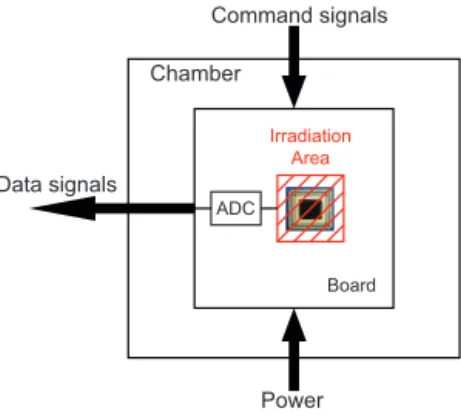
subtracted to cancel the offset. Power supply was designed by CNES to detect SEL and protect the sensor integrity if necessary. The threshold was set to twice the nominal current consumption of the board (during dark frames acquisition). The command and address signals were generated by a FPGA board away from the beam. The proximity board (carrying the chip) was placed in front of the beam, and signals were digitized on this board before being sent to the acquisition computer. The ADC and all other components from proximity board were not irradiated thanks to a keep-out area around the sensor. Thus only the chip itself was exposed as seen on Fig. 2. Power Command signals Chamber Irradiation Area Board Data signals ADC
Fig. 2. Schematic of experimental setup
B. Irradiation conditions
A part of measurements were performed at the Catholic University of Louvain-La-Neuve in Belgium. The facility can deliver a cocktail of different species of ions with different energies. The ranges of Linear Energy Transfer (LET) are shown in Fig. 3. All measurements were done inside a vacuum chamber.
Investigations on SEL were performed with maximum LET available in the facility which corresponds to 67.7 MeV.cm²/mg. Then one chip was tested under different ions
0 10 20 30 40 50 60 70 80 90 0 10 20 30 40 50 60 70 Depth (µm) L ET (Me V. cm²/ mg ) Kr Ganil Xe Kr Ar N
Fig. 3. LET in Silicon vs depth for each ion and facility.
to check its influence over charge collection in the pixel. A second set of data was performed at the “Grand accélérateur National d’Ions Lourds” (GANIL) in Caen, France. The
facil-ity delivers a86
36Kr ion with an energy of 8.87 MeV/A passing
through an HAVAR®window of 4.445 µm and air. Simulation
of end beam properties was made with SRIM software [11]. Final energy is 611 MeV, and LET is 35.5 MeV.cm²/mg. The angle between devices and ion flux was normal in all experiments and for all ions.
III. RESULTS AND DISCUSSIONS
The first part of this work covers the identification of the possible SEEs and their sub-circuit location. Different physical effects can be triggered by an incoming ion, and each part of the circuit can have different sensibilities for a given SEE. Therefore, the sensor can be treated at the system level divided into three parts: the X and Y decoders, the pixels and the analog readout circuits. Each part can be sensitive to particular SEEs, as summarized in Table I. The address decoder is not latched. Address signals have to be kept connected during each sequence. Consequently, the transient events cannot be latched and the address is only temporarily disturbed if struck by an ion. However, the use of PMOS and NMOS transistors in close proximity make this circuit vulnerable to Single Event Latch-Up (SEL); which can be potentially destructive if the circuit is not protected [12]. Pixels, which contain the photosensitive area, are the key elements. Although they are not susceptible to SEL (only NMOST are used in the studied pixels) the ‘integration’ mode makes them accumulate excess charges. It includes photo-generated signal and ion-matter interaction generated charges. Single Event Transient (SET) generates more charge than visible light in a pixel, and can degrade the image quality, leading to saturation and blooming.
Since ion flux control and image capture are not synchro-nized, an ion can strike the device at any time during the readout cycle. Yet all timing cases must be considered to obtain a full list of possible events. The sensor works in
TABLE I SEES IN THE SENSOR
Ion Single Event
Effects Short description Will happen experimentally Pixel Array Single Event Transient (SET) Diode integrates transient current Yes, with variable magnitude depending on the sensor Address Decoder Single Event Latch-up (SEL) Latch of parasitic thyristor, possibly destructive No, according to worst case TCAD simulation Single Event Disturb (SED) Transient disturb of pixel addressing
Yes, with low probability due to small decoder area Readout Circuits Capacitor and ALL transistors Single Event Gate Rupture (SEGR) Single Event Dielectric Rupture (SEDR) Thin oxides can be ruptured by a single ion.
No, ion used here are not heavy enough to produce significant dielectric variations (1 nm bump against 10 nm oxides) [13], [14]
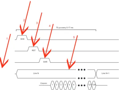
rolling shutter mode with a total readout time of 9.17ms; which means that each line is read and initialized successively. Command signals are first sent to all the pixels of the line: signal sampling, reset and reference sampling (Non-Correlated Double Sampling). Then, sampling capacitors of each row readout circuits are connected to the output, as seen in Fig. 1. Photodiodes of the line integrate charges between each reset and sampling signal, meaning the time during the readout of the other lines of the array. In our case, integration time is 9.17ms, no integration time is added to array readout time.
SHS RST SHR Line N Line N+1 Column 1 2 3 127 128 70 µs every 9.17 ms 4 5 6 1 2 3 4 5
Fig. 4. Chronogram of line readout. SHS and SHR represents signal and reference sampling.
If an ion strikes during the integration phase in a location far under the current read line (case 1 on Fig. 4), all the surrounding pixels will collect diffused charges and the entire
cluster will be present on the frame. If an ion strikes near a line being read (case 5), the current line will stay black (signal sampling occurs at the beginning of each line cycle), and next the line samples the collected charges. The resulting frames are shown in Fig. 5; only the bottom part of the pixel cluster appears on the current frame, and the next one shows only the upper part of the cluster.
10 20 30 40 5 10 15 20 25 30 35 40 0 5000 10000 15000 10 20 30 40 5 10 15 20 25 30 35 40 0 2000 4000 6000 8000 10000 12000 14000
Fig. 5. Case 5: successive frames of a cut cluster (Digital Units). Full cluster can be rebuilt with both frames.
Cases 2, 3 and 4 describe the effect of ion hitting on the line during command signals. These cases are the less probable (total time is less than 10% of the readout phase). The only impact of an ion strike in these cases is corruption on signal, reference, or reset on one line. Therefore, they are neglected. In order to study the charges collected by clusters of pixels, it is important to use full clusters. Rebuilt ones may have corrupted information on the line that was being read when the ion struck.
A. Addressing decoders
These sub-circuits are built with non-latched CMOS de-coders. Since they are not latched, they are exposed to Single Event Disturbs (SED) and no upset (SEU or MBU) can be observed. These parts are also built with PMOS and NMOS transistors within a small area, forming parasitic thyristors which are the key element for Single Event Latch-up (SEL) triggering [12].
Prior experiments, a test structure[15] was simulated with Sentaurus TCAD software. Fig.6 presents the current in this structure for several cases using higher LET than in experi-ment. Parasitic thyristor was triggered only for higher supply voltage than maximum operating allowed in our APS. No current latch was observed with measured doping profiles and minimum technology rules for the maximum LET particle. Nevertheless, a detection and protection supply have been used for the first experiment with the worst case scenario: bulk substrate chip and particle with maximum LET. No triggering
was detected at a fluence of 3.7 × 10⁶ particle/cm−2, unlike
what is presented in [8]. The mean number of hit for this fluency is 24, so probability of latch-up is below 4% for one decoder and SEL was not considered an issue. The supply was thus replaced by a standard one for the other ions and GANIL experiment.
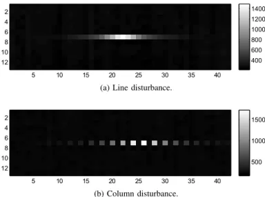
The collection of charges on transistor nodes induced tran-sient potential variations. In such a case the selection line can be affected, and a transient address jump can occur on either line or column. Both of these events have been observed as seen in Fig. 7.
3.3V 10V
Time (s)
0 5e−08 1e−07 1.5e−07 2e−07
C u rr e n t (A ) 0 0.01 0.02 0.03 0.04 0.05
Fig. 6. Simulated current through test structure electrodes during an ion strike. The LET of the incoming particle is higher in this simulation than in the experiment. Supply voltage is set similar to experiment for the line with square markers and is bigger for the line with round markers. Triggering is considered when current stays higher than equilibrium value during long times (all simulation time i.e 1ms). Line with square markers does not trig, so the required conditions are worse than in the experiment.
5 10 15 20 25 30 35 40 2 4 6 8 10 12 400 600 800 1000 1200 1400
(a) Line disturbance.
5 10 15 20 25 30 35 40 2 4 6 8 10 12 500 1000 1500 (b) Column disturbance.
Fig. 7. Transient events on addressing decoders. Frame represents digital unit of measured output voltage for each pixel. These transient events happen both in array and addressing decoder.
The event is only temporary because no latch is present in the decoder circuit. All signals commands are held by circuitry outside the chip, which is not exposed in our measurements.
B. Readout circuit
The readout circuitry, presented in Fig. 8, is immune to latch-up since NMOS and PMOS transistors are separated by a capacitor representing a large area (several microns on
the chip)1. The capacitor is made of poly-silicon separated
from the substrate. It is thus immune to transients and cannot collect charges from the substrate. Of course node connected to transistors can have transient currents, affecting temporarily the output node. The sampling capacitance is about 10pF and the current in transistor nodes can increase potential. However, the command signal are connected for a longer time (~1µs) than collection time, so the capacitance will discharge into a supply rail. Therefore, the probability that an event occurs and is sampled is very low, and it would only affect one pixel corresponding to the struck node.
Vsig x
Signal sampling SHS/SHR
Symmetrical circuit for reference signal Bias Bias Csig +V +V +VDDrst RST T1 T2 T3 Y Pixel
Fig. 8. Readout circuit schematic. First part is NMOST only and second PMOST only.
C. Pixels
The different pictures show charge collection with clusters of pixels. These clusters have different sizes and saturation levels depending on the type of incident particles (LET), and the structure of the photodiode in the pixel, as seen in Table II. The charge collected by these pixels are discussed in the next section.
IV. CHARGE COLLECTION
The deposited charges are collected by each floating pho-todiode, forming cluster of white pixels on final frames. The size and total collected charges are important parameters and must be known to make predictions and to help instrument and sensor designers to take into consideration the SEE constraint. They depend on incident LET of the particle and its range in the Silicon. In the next section, we will study total charge collected, followed by model assessment and discussion on blooming. The last section will analyze variations of substrate and photodiode design.
A. Data
The collected charge in a cluster were extracted by summing the signal value of each pixel. Comparison with charges 1The distance between PMOS and NMOS transistors is linked to the base
width of parasitic bipolar transistors. An increase of this distance reduces the triggering sensitivity of the structure.
TABLE II
CLUSTER PROPERTIES OF EACH CHIP
Experiment and ion APS Ion LET (MeV.cm²/mg) Diameters of circular clusters (disturbed pixels) Added counts (electrons)
UCL APS1 124Xe 67.7 12 1.772 × 10⁷ 84Kr 40.4 10 1.322 × 10⁷ 40Ar 15.9 9 7.960 × 10⁶ 15N 3.3 8 3.657 × 10⁶ GANIL APS1 86Kr 35.5 18 3.058 × 10⁷ APS2 86Kr 35.5 3 3.356 × 10⁶
deposited by a particle can give information on collection process. The number of pixels (i.e. the cluster size) used for the sum was increased to determine the total collected charge, as presented in Fig. 9. When the curves reach a plateau, all the charge is collected.
2 4 6 8 10 12 14 16 18 20 0 0.5 1 1.5 2 2.5 3 x 10⁷ Pixel Index N u mb e r o f co lle ct e d e le ct ro n s Xe Kr Ar N Kr GANIL Kr GANIL Epi
Fig. 9. Total charge in a cluster as a function of the cluster width for APS1. The Y-axis value gives the total collected charge when a curve reaches the plateau.
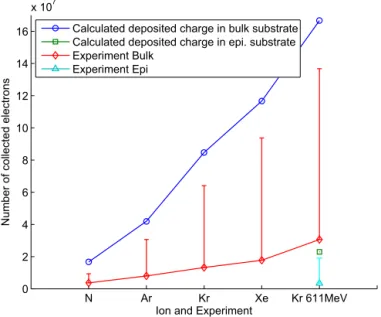
The size of a cluster is a consequence of electron diffusion in the silicon. Therefore, it should be linked to the charge deposited by the incident particle. The number of carriers created can be estimated by the total energy of the particle divided by the mean energy required to produce electron-hole pairs [16]. Considering this process linear, a direct relation can be made with each particle energy. Thus, if one assumes that all the deposited charge is collected by the nearest pixels, the number of collected charge can be forecasted. This estimation works only if the particle stops inside the sensitive layer. It means that this calculation should overestimate the number of collected electrons for epitaxial layer case since the particle ranges used in this study are longer than the epitaxial layer thickness. Fig. 10 presents the number of collected electrons estimated with this calculation, compared with the measured collected charges for both cases (bulk and epitaxial layer of 7µm). This first order calculation can be refined to take into account the reduced sensitive volume of the device built with an epitaxial layer. In this case, the sensitive depth is assumed to be equal to the thickness of the epitaxial layer. The
number of deposited charges into this layer can be evaluated by integrating the particle LET over its thickness. The results are shown in Fig. 10. For most of the cases, this refined calculation still overestimates all experiments. Two effects can explain this discrepancy. The first one is the impossibility to measure correctly the charge in saturated pixels. In such pixels, the readout chain gets saturated before the photodiode which continues to collect charges whereas the output voltage is fixed, causing an underestimation of the collected charge. This effect is illustrated in Fig. 12 which presents the input and output of the readout circuits versus injected charge in the diode. N Ar Kr Xe Kr 611MeV 0 2 4 6 8 10 12 14 16 x 107
Ion and Experiment
N u mb e r o f co lle ct e d e le ct ro n s
Calculated deposited charge in bulk substrate Calculated deposited charge in epi. substrate Experiment Bulk
Experiment Epi
Fig. 10. Total charge collected in clusters with 10µm pitch pixels. Experi-ments are represented by diamonds and triangles (APS1 and 3). The error bars show the estimation of the charges lost due to the readout circuit saturation.
The number of saturated pixels increases with deposited energy, as seen on profiles of Fig. 11, leading to the underes-timation of the total number of collected charges. The second cause for a discrepancy is the non ideal collection efficiency (i.e. <1). Because of recombination of excess carriers in silicon, the greater the distance from ion trace, the lower is the fraction of collected charge.
This section has shown the need to consider the readout chain saturation when the total collected charge need to be measured. This saturation is also important at the pixel level, when measured cluster profiles are compared to a model, as discussed in the next section.
−200 −15 −10 −5 0 5 10 15 20 2 4 6 8 10 12 x 104 Pixel Index N u mb e r o f co lle ct e d e le ct ro n s Xe Kr Ar N Kr GANIL Kr GANIL Epi
Fig. 11. Radial cluster profile for all ions on bulk substrate and pixels of 10 microns (APS1). A profile of GANIL experiment with a CIS using the same pitch and an epitaxial substrate (APS3) is shown with “+” markers.
0 0.5 1 1.5 2 2.5 x 10⁵ 0 0.5 1 1.5 2 2.5 3 3.5
Number of electrons injected
Po te n ti a l (V) Vref−Vdiode Vref−Vsig
Fig. 12. Output signal Vsig) is compared to readout input (Vref-Vdiode) when electrons are injected in the diode. Reference potential is 3.3V and the model use diode equation and experimentally determined readout transfer function.
B. Model assessment
To predict single event induced pixel collection when CIS are exposed to ionizing particle, we decided to use the STAR-DUST software [17], [18]. It predicts the collection of carriers by all pixels of an array. It is based on particle interactions in a sensitive volume surrounded by a diffusive substrate. Even though it does not account for diode saturation and blooming, the effects are not significant on the results (for 3T pixels and bulk substrates, see IV-C). Thus only the saturation effect has to be taken into account simply by the truncation of the simulated values when they reach the readout circuit saturation level. Fig. 13 presents the profiles of cluster of pixels for four different ions compared with truncated simulations. The
simulated data (without any fitting parameter) is showing a correct order of magnitude and shape but some overestimation can be seen on the cluster edges. The input parameters of the software are physical and technological. They are not well known since they require a good knowledge of material and fabrication process. Thus the discrepancy must be attributed to one or several these parameters.
−200 −10 0 10 20 5 10 x 104 Xe N u mb e r o f co lle ct e d e le ct ro n s −200 −10 0 10 20 5 10 x 104 Kr −200 −10 0 10 20 5 10 x 104 Ar Pixel Index N u mb e r o f co lle ct e d e le ct ro n s −200 −10 0 10 20 5 10 x 104 N Pixel Index 0 50 100 150 200 0 50 100 150 200 R e la ti ve Erro r (% ) 0 50 100 150 200 0 50 100 150 200 R e la ti ve Erro r (% )
Fig. 13. Data (APS1) and simulations for different species of ions with decreasing LET. Point marked lines are simulations, plus marked lines are experimental data, Y-scales are on the left. Cross marked lines are relative error, Y-scale is on the right.
As seen in Fig. 13, the error between STARDUST simula-tion and the measured data increases with distance from the ion trace. Among the possible cause for these discrepancies we can name: an error on the particle energy or passive layer thickness estimation. Error on the estimated depletion region thickness could also be involved but it would have only little effect on diffused charges. An inaccurate diffusion length is the only parameter that has a larger impact on the most distant pixels from the strike. Unfortunately, doing a fit with this parameter on one ion increases errors on the other ions. Thus one or several other parameter, or the model itself, must differ and work have to be done in the future to improve the model accuracy by finding the parameter (or parameters) involved.
C. Effect of blooming
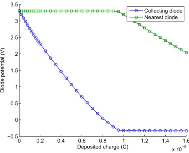
We talked about blooming in precedent section. Fig. 14 is extracted from a 2D Sentaurus TCAD simulation to illustrate this effect - which happens when pixels are overexposed. One diode is collecting charges and the other is left floating. When the first one reaches equilibrium, the additional charges diffuse into neighboring diodes (only one of them is shown for clarity purpose) and their potential start to reduce.
In our case, this phenomenon could appear at the edges of clusters where saturated diodes let charge diffuse in non saturated ones. But the saturation level of the readout circuit is at least partially masking this effect. Fig. 12 shows the readout circuit output when charges are injected in the diode. Clearly, the output signal saturates before the diode potential reach
0 0.2 0.4 0.6 0.8 1 1.2 1.4 1.6 x 10⁻⁶ −0.5 0 0.5 1 1.5 2 2.5 3 3.5 Deposited charge (C) D io d e p o te n ti a l (V) Collecting diode Nearest diode
Fig. 14. Graph of a TCAD simulation of two adjacent diodes. The potential fall with charge deposition. The generation occurs in the depletion region of the diode, until it reaches a negative potential (almost null space-charge region). This situation is only temporary, diode tends to a null potential in the next µs.
its maximum. The difference on the X-axis give us the total charge that the diode collected after readout circuit is saturated. Fig. 13 show the trend of a peak distribution with a saturated
level about 105 electrons, which is the saturation level of the
readout chain. The knowledge of the visibility of the blooming effect on the output is important for mitigation purposes. First, an estimation of the cluster of deposited charges is needed, i.e. its amplitude and its shape. The Gaussian assumption is used since the charge density resolution in low-level injection
is based on spatial Gaussian function: exp(−4Dtr2 − t
τ) [19].
There is a small error in cluster edge which can be neglected since the particle induced electrons are difficult to discriminate from total number of electrons (background electrons). This fit is used to analyze blooming.
Blooming effect is the diffusion of carriers which are not collected in saturated photodiode into the neighboring pho-todiodes. We assume charge conservation and homogeneous diffusion in the radial profile (1D). Thus the worst case (no recombination) is considered. Fig. 15 shows the differences between data, the Gaussian fit, and the estimation of charges collected by the photodiodes (green cross points), which account for blooming. This effect is limited to 1 or 2 pixel in radius. Hence, it is not significant and the use of an anti-bloooming circuit would be useless to mitigate SET in this case.
D. Design variations
1) Pixel width and length: Fig. 16a presents the measured
and simulated Kr (GANIL) induced cluster profile on two APS on bulk substrate with different pixel pitches (7 and 10 µm). First, as concluded in section IV-B, the STARDUST simulations agree well with both measurements. It shows once again that simulating ideal sensors (array of pixels with 100% fill factor and no MOSFET) is sufficient to predicts the cluster profile on bulk substrate, even when the pixel pitch is changed.
−200 −15 −10 −5 0 5 10 15 20 0.5 1 1.5 2 2.5x 10 5 Pixel index N u mb e r o f co lle ct e d e le ct ro n s Gaussian fit Data
Diode saturation level Blooming
Readout saturation level
Fig. 15. The data of APS1 under GANIL (Kr) experiment are fitted with a Gaussian function. Dotted line is the diode saturation level. Green crosses are calculated with blooming: charge not collected by saturated diode diffuse into non saturated ones.
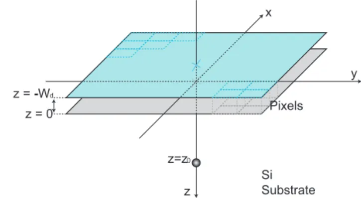
In the simulation software the total sensor space-charge region is considered as an ideal rectangle cuboid volume subdivided into rectangular pixels as shown in Fig. 17. Since this model does not take into account the drop in photodiode bias voltage with collected charges, the simulated density of collected charge per unit area should be exactly the same whatever the pixel pitch. In other words, whatever the number of pixels, from the diffusion process point of view, the electron cloud always sees the same uniform space charge region on the whole sensor (independently of the number of pixels). This conclusion has been verified in Fig. 16b by plotting the density of collected charges per unit area (by dividing by the pixel area). It shows that, as expected, the simulation yield exactly the same results when expressed in charge density per unit area. This normalization by pixel area also shows that there is no more difference in measured cluster profiles. Therefore, it can be concluded that, as far as blooming effects are hidden by the readout chain saturation, pixel pitch variations (and thus photodiode size) have no effect on the cluster profile in bulk substrate sensors (simulated and measured). The distribution of charge density per unit area is not influenced by the pixel dimensions. It should be emphasized that the pixel area must be used for the normalization, not the photodiode (i.e. space charge region) one.
2) Photodiode layout variations: In this section, the case
of hardened photodiode designs is discussed. The matrix used is described in [20]. It contains photodiodes of several types: standard, recessed oxides, surrounded with a P+ doping profile or a gate (grounded). The results are presented in Fig. 18. The difference between each device is only due to the modification of the capacitance. The more the capacitance increases, the more the sensitivity decreases and the saturation charge increases. The only difference between standard diodes and all the other designs is the saturation level. The shape and width of profiles is exactly the same. Moreover, the simulation
−150 −100 −50 0 50 100 150 0 2 4 6 8 10 12 14x 10 4 Length (µm) N u mb e r o f co lle ct e d e le ct ro n s Simu. pitch 7 µm Simu. pitch 10 µm APS1 bulk px 7 µm APS4 bulk px 10 µm
(a) Mean radial profile of clusters formed in each array. X-axis shows the common physical profile in micrometers for APS1 (7µm pitch pixels) and APS4 (10µm pitch pixels). The capacitances of the two pixels are different (9.2 fF for APS1 and 10 fF for APS4), which explains the difference between the two saturation levels. −2000 −150 −100 −50 0 50 100 150 200 500 1000 1500 2000 2500 3000
Distance from ion impact point (µm)
D e n si ty o f co lle ct e d e le ct ro n s (e -/ µ m²) simu. Pitch 7µm simu Pitch 10µm data APS1 data APS4
(b) Normalized number of collected electrons per pixel, for APS1, APS4 and simulations with a bulk substrate.
Fig. 16. Mean profiles and mean normalized profiles for the GANIL experiment (611 MeV Kr ion)
agrees fairly well with the data, except in saturated pixels; showing that device variations around the photodiode have no significant effect on SET, contrary to results presented in [7]. It is interesting to note that despite the different capacitances of the standard and hardened diodes, all the experiments have the same profile. It means a modification of the maximum capacity of the diode to collect electrons does not affect the charge collection, confirming the discussion of section IV-C on blooming and IV-D1 on photodiode dimensions.
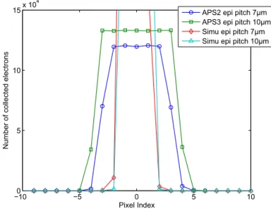
E. Substrate variations : effect of an epitaxial layer
Fig. 19 shows the mean profile of the clusters for different arrays. The use of an epitaxial layer with high resistivity, on top of a highly doped bulk silicon, allows to recombine these carriers (low diffusion length). Therefore, the cluster
z = -W z=z0 d z = 0 y z x Si Substrate Pixels
Fig. 17. The space between the two planes is the space charge region (of thickness Wd). Positive z-axis direction is the Silicon substrate, with a source
point generating charges.
−200 −15 −10 −5 0 5 10 15 20 0.5 1 1.5 2 2.5x 10 5 Pixel Index N u mb e r o f co lle ct e d e le ct ro n s Standard Recessed oxydes P+ surrounded Gated (ground) Simulation 10µm Bulk
Fig. 18. Diode collection profiles under GANIL experiment. Device uses bulk technology and 10 µm pitch pixels (APS4). Non-standard diodes are recessed oxides, transistor, gate, and P+ surrounded with the same conversion gain (i.e. same diode capacitance) of 10 µV/electron. Standard diode has a different CVF of 17 µV/electron. The line with triangular markers (not saturated) is the result of the STARDUST simulation software.
radial profile obtained have a sharpened edge with a similar saturation level. These levels are not exactly the same because of sensitivity differences of the two designs.
In this case, the simulation does not render correctly the profile shape, and the normalization of results does not produce similar curves. The model used only accounts for diffused electrons in the substrate. Discrepancy can come from several causes. Model uses diffusion of charges in the epitaxial substrate and does not account for deep highly doped substrate. A part of charges generated in this deep region
might be collected. A 1018cm−3P-type Silicon material has
a diffusion length of several micrometers. A fraction of the charges generated in the first micrometers of the region under the epitaxial layer could diffuse and reach the photodiodes. Another cause is the blooming effect (discussed in IV-C) which could be visible despite the readout circuit saturation level if the deposited charges follow a sharper Gaussian function. These effects have to be investigated to improve the
−100 −5 0 5 10 5 10 15x 10 4 Pixel Index N u mb e r o f co lle ct e d e le ct ro n s
APS2 epi pitch 7µm APS3 epi pitch 10µm Simu epi pitch 7µm Simu epi pitch 10µm
Fig. 19. Different profiles obtained at GANIL experiment (ion Kr) with APS1 and 3 - which use epitaxial layer substrate. The profile of these devices is much sharper than previous experiments. The trend of simulations (diamonds and triangles) poorly agree with the data.
model predictions when epitaxial substrates are used. V. CONCLUSION AND PERSPECTIVES
CMOS image sensors with 3T photodiode pixels have been exposed to a heavy ion flux. No loss of functionality (SEL, SEFI) has been observed due to the simple architecture used (no sequencer, no register, no ADC). Reducing the functions embedded on the device can thus be used as a first approach on hardening. However SET appeared on addressing subcircuits and pixels. SET happening on the addressing circuits are line corruption due to an address jump. Transient events affecting the array of pixels are parameter dependent, the modification of technological and design parameters influences the number of pixels affected and the number of charge collected. The pixel pitch does not reduce the real physical dimensions of the cluster, but we have shown that the use of an epitaxial layer reduces the cluster spread and charge collection. However photodiode design variations have no visible effects when technology uses a bulk substrate. The variations on epitaxial substrates need to be investigated since the cluster profile is much sharper and surface, substrate or blooming effects could be visible. We have also shown that STARDUST simulation software is useful to predict SET on the pixel array for several ions. The model does not account for saturation since blooming effects are hidden by the readout chain saturation, but a simple truncation at this level gives good results if the use is limited to bulk substrate technology. The investigation of model and experiment discrepancy on epitaxial technology have to be further studied to improve model predictions.
The results presented here can be transposed to any “more-integrated CIS”, such as “smart sensor”, or imager with on-chip analog-to-digital converters, provided that the pixels are 3T based on a conventional photodiode. In these cases, the additional effects induced by added circuits need to be taken into account (e.g. SEL, Single Event Upset in digital circuits, ...).
ACKNOWLEDGMENT
The author would like to thank the CIMI group for their great help, especially Paola Cervantes for software and hard-ware implementations, Barbara Avon for characterizations, Franck Corbière for discussions. The author would also like to thank Françoise Bezerra (CNES) and Marc Gaillardin, Mélanie Raine (CEA) who provided beam time and support. Final thanks go to Cédric Virmontois (CNES), Guy Berger (UCL), Emmanuel Balanzat (GANIL), Guillaume Hubert (ONERA) who provided support during measurements.
REFERENCES
[1] G. L. Keister and H. V. Stewart, “The effect of nuclear radiation on selected semiconductor devices,” Proceedings of the IRE, vol. 45, no. 7, p. 931–937, 1957.
[2] E. Fossum, “Digital camera system on a chip,” Micro, IEEE, vol. 18, no. 3, pp. 8 –15, Jun. 1998.
[3] T. S. Lomheim, R. M. Shima, J. R. Angione, W. F. Woodward, D. J. Asman, R. A. Keller, and L. W. Schumann, “Imaging charge-coupled device (CCD) transient response to 17 and 50 MeV proton and heavy-ion irradiatheavy-ion,” Nuclear Science, IEEE Transactheavy-ions on, vol. 37, no. 6, p. 1876–1885, 1990.
[4] G. Deptuch, J.-D. Berst, G. Claus, C. Colledani, W. Dulinski, Y. Gor-nushkin, D. Husson, J.-L. Riester, and M. Winter, “Design and testing of monolithic active pixel sensors for charged particle tracking,” Nuclear Science, IEEE Transactions on, vol. 49, no. 2, pp. 601–610, 2002. [5] G. Hopkinson, A. Mohammadzadeh, and R. Harboe-Sorensen,
“Radia-tion effects on a radia“Radia-tion-tolerant CMOS active pixel sensor,” Nuclear Science, IEEE Transactions on, vol. 51, no. 5, pp. 2753–2762, 2004. [6] X. Belredon, J. P. David, D. Lewis, T. Beauchene, V. Pouget, S. Barde,
and P. Magnan, “Heavy ion-induced charge collection mechanisms in CMOS active pixel sensor,” Nuclear Science, IEEE Transactions on, vol. 49, no. 6, p. 2836–2843, 2002.
[7] C. J. Marshall, K. A. LaBel, R. A. Reed, P. W. Marshall, W. B. Byers, C. Conger, J. Peden, E. S. Eid, M. R. Jones, S. Kniffin et al., “Heavy ion transient characterization of a hardened-by-design active pixel sensor array,” in Radiation Effects Data Workshop, 2002 IEEE, 2002, p. 187–193.
[8] P. Vu, B. Fowler, J. Balicki, C. Liu, S. Mims, H. Do, W. Li, J. Appel-baum, H. Venus, H. Schwarzer, X. Amigues, P. Becker, K.-H. Degen, and M. Neidhardt, “High-speed BSI CMOS image sensor for space applications with 1.1Me- full well capacity and 28e- rms read noise,” in Workshop “CMOS Image Sensors for High Performance Applications”. Toulouse: CNES, Dec. 2011.
[9] C. C. Liebe, S. Mobasser, Y. Bae, C. J. Wrigley, J. R. Schroeder, and A. M. Howard, “Micro sun sensor,” in Aerospace Conference Proceedings, 2002. IEEE, vol. 5, 2005, p. 5.
[10] V. Goiffon, S. Girard, A. Chabane, P. Paillet, P. Magnan, P. Cervantes, P. Martin-Gonthier, J. Baggio, M. Estribeau, J.-L. Bourgade, S. Darbon, A. Rousseau, V. Y. Glebov, G. Pien, and T. C. Sangster, “Vulnerability of CMOS image sensors in megajoule class laser harsh environment,” Optics Express, vol. 20, no. 18, pp. 20 028–20 042, Aug. 2012. [11] J. Ziegler, “SRIM & TRIM software.” [Online]. Available: http:
//www.srim.org
[12] R. R. Troutman, Latchup in CMOS technology: the problem and its cure. Springer, 1986.
[13] M. Toulemonde, C. Trautmann, E. Balanzat, K. Hjort, and A. Wei-dinger, “Track formation and fabrication of nanostructures with MeV-ion beams,” Nuclear Instruments and Methods in Physics Research Section B: Beam Interactions with Materials and Atoms, vol. 216, pp. 1–8, Feb. 2004.
[14] A. Touboul, J. Carlotti, M. Marinoni, M. Caussanel, M. Ramonda, C. Guasch, G. Bruguier, J. Bonnet, F. Saigné, and J. Gasiot, “Growth of heavy ion-induced nanodots at the SiO2–Si interface: Correlation with ultrathin gate oxide reliability,” Journal of Non-Crystalline Solids, vol. 351, no. 52-54, pp. 3834–3838, Dec. 2005.
[15] G. Bruguier and J. M. Palau, “Single particle-induced latchup,” Nuclear Science, IEEE Transactions on, vol. 43, no. 2, p. 522–532, 1996. [16] R. C. Alig, S. Bloom, and C. W. Struck, “Scattering by ionization and
phonon emission in semiconductors,” Physical Review B, vol. 22, no. 12, pp. 5565–5582, Dec. 1980.
[17] G. Rolland, L. Pinheiro da Silva, C. Inguimbert, J.-P. David, R. Ecoffet, and M. Auvergne, “STARDUST: a code for the simulation of particle tracks on arrays of sensitive volumes with substrate diffusion currents,” IEEE Transactions on Nuclear Science, vol. 55, no. 4, pp. 2070–2078, Aug. 2008.
[18] G. Rolland, “New analytical solutions of the diffusion equation available to radiation induced substrate currents modeling,” IEEE Transactions on Nuclear Science, vol. 55, no. 4, pp. 2028–2035, Aug. 2008.
[19] S. M. Sze and K. K. Ng, “Physics of semiconductor devices,” in Physics of semiconductor devices. John Wiley and Sons, 2007, pp. 66–67. [20] V. Goiffon, P. Cervantes, C. Virmontois, F. Corbiere, P. Magnan, and
M. Estribeau, “Generic radiation hardened photodiode layouts for deep submicron CMOS image sensor processes,” Nuclear Science, IEEE Transactions on, vol. 58, no. 6, p. 3076–3084, 2011.