O
pen
A
rchive
T
oulouse
A
rchive
O
uverte (
OATAO
)
OATAO is an open access repository that collects the work of Toulouse researchers
and makes it freely available over the web where possible.
This is a publisher-deposited version published in:
http://oatao.univ-toulouse.fr/
Eprints ID: 3240
To link to this article: DOI:
10.1109/TED.2009.2030623
URL:
http://dx.doi.org/10.1109/TED.2009.2030623
To cite this version: GOIFFON, Vincent. ESTRIBEAU, Magali. MAGNAN, Pierre.
Overview of ionizing radiation effects in image sensors fabricated in a
deep-submicrometer CMOS imaging technology. IEEE Transactions on Electron Devices, vol.
56, n° 11, pp. 2594 -2601. ISSN 0018-9383
Any correspondence concerning this service should be sent to the repository administrator:
Overview of Ionizing Radiation Effects in Image
Sensors Fabricated in a Deep-Submicrometer
CMOS Imaging Technology
Vincent Goiffon, Member, IEEE, Magali Estribeau, and Pierre Magnan, Member, IEEE
Abstract—An overview of ionizing radiation effects in imagers
manufactured in a 0.18-µm CMOS image sensor technology is presented. Fourteen types of image sensors are characterized and irradiated by a60Co source up to 5 kGy. The differences between these 14 designs allow us to separately estimate the effect of ioniz-ing radiation on microlenses, on low- and zero-threshold-voltage MOSFETs and on several pixel layouts using P+ guard-rings and edgeless transistors. After irradiation, wavelength dependent responsivity drops are observed. All the sensors exhibit a large dark current increase attributed to the shallow trench isolation that surrounds the photodiodes. Saturation voltage rises and read-out chain gain variations are also reported. Finally, the radiation hardening perspectives resulting from this paper are discussed.
Index Terms—Active pixel sensors (APSs), CMOS image
sensors (CISs), dark current, ionizing radiation, microlenses, quantum efficiency, radiation hardening by design, responsivity, total dose.
I. INTRODUCTION
I
MAGE sensors based on CMOS manufacturing process are now used in a wide variety of applications. Compared to charge-coupled devices (CCD), CMOS image sensors (CISs) have several intrinsic advantages such as low power consump-tion, random access of image data, the possibility to integrate on-chip and even in-pixel advanced functionalities, immunity to blooming and smearing, and high miniaturization potential. Recent advances in CMOS manufacturing processes dedicated to imaging, also called CIS technologies, have allowed CISs to reach CCD image quality. Thanks to all these features, CIS are now good candidates in demanding applications such as medical imaging, particle detection, and space remote sensing. In all these particular applications, image sensors are meant to be exposed to high doses of ionizing radiation.Important efforts have been made to understand and signif-icantly reduce the effect of ionizing radiation on CISs in the last decade [1]–[6]. However, the use of deep-submicrometer technologies dedicated to imaging have brought new behaviors [7], [8] that needs to be studied more in detail, particularly at total ionizing dose above 1 kGy.
Fig. 1. Illustration of the readout path of the studied CISs, from the photodi-ode to the analog output.
In this paper, we present a study of ionizing radiation effects, up to 5 kGy, in several CISs manufactured using a commer-cial 0.18-μm technology dedicated to imaging. Several pixel
layouts and readout chain designs have been used to reveal the degradation origins. This analysis also relies on previous work on dedicated test structures, such as isolated photodiodes and MOSFETs [8]. After describing the experimental details, such as the specificities of the image sensors used and the irradiation details, the effects of ionizing radiation on the sensor performances are presented and discussed. Finally, the last section presents some recommendations for radiation hardening by design.
II. EXPERIMENTALSETUP
A. Sensor Details
Fourteen pixel arrays have been designed and manufactured in several lots using a CIS 0.18-μm process dedicated to
imag-ing (from UMC). The pixel type used is a photodiode-based active pixel sensor (APS) architecture with three transistors per pixel (3T APS architecture). All the transistors used in the design are 3.3-V compliant. The readout path, from the photodiode to the sensor analog output, is shown in Fig. 1. Only one-half of the double sampling stage is represented for more clarity. This readout path first includes three in-pixel n-channel MOSFETs: N1, N2, and N3 for reset, amplification, and se-lection purpose, respectively. Each pixel output is connected through the column bus to an NMOST-based current source and a simple sample-and-hold stage. The remaining part of the circuit is composed by p-channel MOSFETs: P1, P2, and P3 for amplification, pixel selection, and biasing purpose, respectively.
TABLE I
SUMMARY OFSTUDIEDSENSORCONSTITUTIONS
Fig. 2. PIX sensor photodiode layouts. (a) Standard CIS photodiode. (b) RFD diode with RFD. (c) Photodiode with surrounding P+guard-ring. The distance d between the STI and the photodiode N implant is also indicated in (b).
Among these sensors, one is the reference device (REF imager), one is similar to the reference device but has one microlens array on top (μLENS imager), eight sensors integrate
several types of transistors in their readout chain (RD imagers), and finally, four sensors differ by their pixel layout (PIX imagers). The main differences between all these pixel arrays are summarized in Table I. The pixel pitch is 10μm in all the
sensors except theμLENS one, which has a 7-μm pixel pitch.
All the studied pixel arrays are made of 64× 64 pixels except REF andμLENS which have 128 × 128 pixels.
Four different MOSFET structures have been used to de-sign these devices: standard transistor (StdVt), low-threshold-voltage transistor (LowVt), MOSFETs with threshold low-threshold-voltage close to zero (0Vt), and enclosed layout transistor (ELT).
In addition to these MOS devices, four photodiode layouts have been designed (Fig. 2): the standard photodiode dedicated to CISs, the same CIS photodiode but with recessed field oxides (RFDs), the CIS diode with a surrounding P+guard-ring (CIS-Pgr), and finally, an RFD diode also with a P+ guard-ring (RFD-Pgr). The recessed distance d between the N implant
mask and the field oxide is about 0.3μm.
Table II summarizes the key electrical characteristics of the studied sensors.VD(Soft) is the maximum photodiode cathode
voltage before entering in soft reset (SR) mode (see next section for further details on reset mode). CVFpdstands for photodiode
charge to voltage conversion factor,Grd is the readout chain
electrical gain defined by ΔVout/ΔVD at VD= VD(Soft),
and Idark is the dark current before irradiation. The junction
perimeter is also presented in the last column.
B. Irradiations and Measurements
All the irradiations took place at room temperature at UCL, Belgium, thanks to a panoramic60Coγ-ray source. The dose
rate was about 20 Gy/h, and the maximum total ionizing dose was 5 kGy. The devices were biased and operated during irradiation.
During measurement, two kinds of reset conditions were used. In the regular reset mode, also called SR [9], the reset transistor gate and drain voltages are equal to the supply voltage
VDD= 3.3 V. At the end of an SR, the reset transistor is biased
in subthreshold regime and the photodiode cathode voltage reaches
VD= VDD− Vth+ ΔVsubth (1)
withVththe reset transistor threshold voltage andΔVsubththe
additional voltage depending on the subthreshold current and the time spent in the subthreshold regime. In this paper, we con-sider that the subthreshold current includes the weak inversion current and any other leakage current. The additional voltage
ΔVsubth is not precisely known and depends on photodiode
voltage before the reset operation. Such behavior leads to well-known image lag effects [10].
Image lag can be eliminated by keeping the reset MOSFET gate-to-source voltage above its threshold voltage in order to stay in the linear regime during the photodiode charge. This reset operation is called hard reset (HR) in opposition to the regular SR mode [9]. The measured photodiode cathode voltagesVD(Soft) corresponding to the boundary between HR
and SR modes are presented for each sensor in the second column of Table II. These values show that for a reset gate voltage equal to 3.3 V, a drain voltage VDD−RST= 2.4 V is
sufficient to ensure an HR operation for every imager. In HR mode, the photodiode cathode voltage is equal toVDD−RSTat
TABLE II
STUDIEDSENSORELECTRICALFEATURES
threshold voltage or subthreshold current. This feature is used in the following section to discriminate the contribution of the reset transistor from the other devices in the sensor responses to irradiation.
If not specified otherwise, all the measurements were per-formed in SR mode (VDD−RST= 3.3 V) at 23 ◦C after a 48-h unbiased room temperature storage with the use of a noncorrelated double sampling.
As regards responsivity measurements, bandpass filters (10-nm FWHM), associated with an automated integrating sphere, were used for spectral response measurements. The input photon quantity was determined thanks to a calibrated photodiode.
III. RESULTS
A. Degradation Overview
After the maximum total ionizing dose, the sensors were still fully functional, and no significant degradation appeared in the digital part of the sensor. We will then focus on the analog functions of the sensor in the rest of this paper.
The comparison of the optoelectrical transfer functions be-fore and after irradiation provides a good degradation overview, as shown in Fig. 3. Two obvious changes are induced by ionizing radiation: a large dark signal increase and a saturation voltage rise. As a first approximation, the sensor sensitivity in volts per photon does not seem to be much influenced by the exposure toγ-rays at 650-nm wavelength.
As discussed in the previous section, operating the sensors in HR mode by settingVDD−RSTto 2.4 V allows one to determine
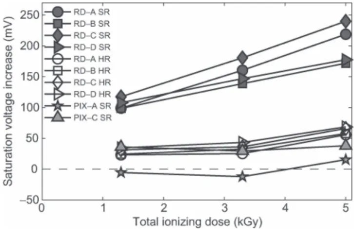
the role of the reset transistor in this saturation voltage rise. Fig. 4 shows this increase as a function of total ionizing dose in SR and HR modes. Only the representative responses are shown for improved clarity. The other devices exhibited similar behaviors.
In SR mode, one can see a steady rise of the saturation volt-age with irradiation on RD sensors. However, in HR mode, the
Fig. 3. Optoelectrical transfer function at 650 nm of the three tested RD-C image sensors, before and after irradiation. The integration time was set to 8 ms, and the devices were operated in SR mode.
Fig. 4. Saturation voltage increase with irradiation for several representative image sensors and for two reset modes: SR and HR.
degradation is significantly reduced (60 mV instead of 240 mV on sensor RD-C) and the saturation voltage does not increase much between 1 and 5 kGy. Hence, the reset transistor appears
to be responsible for the main part of the saturation voltage increase. This is confirmed by the behavior of PIX-C sensor in SR mode which is similar to the other sensor responses in HR. It shows that the use of a radiation hardened reset transistor elim-inates the main part of the degradation. According to (1), all these observations suggest either a radiation-induced decrease ofVth or an increase ofΔVsubthin the reset transistor N1 in
RD sensors (or both). It is interesting to notice that ionizing radiation is known to induce threshold voltage shift in deep-submicrometer MOSFET through charge trapping in shallow trench isolations (STI), on the sides of the transistor channel. This effect is called radiation-induced narrow channel effect (RINCE) [11] and corresponds well to the observed degradation since the use of ELT eliminates the degradation. γ-rays can
also changeΔVsubthby increasing the source-to-drain leakage current and so, by increasing the total subthreshold current. Edgeless transistors, such as ELT, also eliminate this parasitic lateral leakage path.
The remaining saturation voltage variation in HR mode can only be due to a readout chain voltage swing increase. The responsible transistor can be identified more precisely by look-ing at the PIX-A sensor response. The three in-pixel n-channel MOSFETs of this imager are ELTs. The saturation voltage of PIX-A device does not seem to be influenced by the exposure to ionizing radiation in Fig. 4. The use of ELT for N1, N2, and N3 seems to eliminate the saturation voltage variation. This suggests that the 30–60-mV variation observed in HR mode in sensors with standard pixel layout (such has RD sensors) is most likely due to n-channel FETs N2 and N3. It also shows that there is no significant charge trapping in MOSFET gate oxides, as expected in deep-submicrometer MOSFET with thin gate oxides [12].
It is interesting to notice that sensors with a StdVt reset MOSFET (RD-A and RD-C in Fig. 4) exhibit a larger increase than the one with a LowVt reset transistor (RD-B and RD-D) in SR mode. The same effect was observed on RD-E and RD-G in comparison to RD-F and RD-H. These observations suggest that the saturation voltage variation due to the reset MOSFET is slightly reduced by the use of a low-Vth reset
transistor (N1 in Table I) instead of a regular one. Radiation-induced voltage shift is known to be due to a change in flatband voltage [13]. This flatband voltage variation induced by γ-rays is proportional to the oxide (gate oxide or STI
oxide) trapped charge and the effective capacitance between this charge and the channel. Therefore, channel doping density is not supposed to influence radiation-induced threshold voltage shift. The reduced saturation voltage variation observed when using low-threshold-voltage reset transistors is attributed to a smaller change in subthreshold current in LowVt MOSFETs after exposure toγ-rays. This subthreshold current is due to
the parasitic lateral transistor [14], and it depends much on the reset transistor drain-to-source voltage. When the photodiode is reset through a LowVt MOSFET, the final drain-to-source voltage is significantly lower than when a standard MOSFET is used (see the second column of Table I for measured values). As a consequence, the parasitic current induced by the irradiation is smaller in LowVt reset MOSFETs and so is the induced
ΔVsubth.
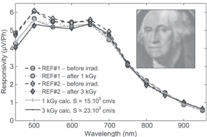
Fig. 5. Responsivity of REF devices prior to and after irradiation, and image captured with the 3 kGy irradiated device. The estimated surface recombination effect on responsivity after irradiation is also shown.
B. Responsivity
Fig. 5 shows the spectral responsivity of two REF devices prior to irradiation and after 1- and 3-kGy irradiations. In order to compute this responsivity, defined here by (2), each device output voltage variation(ΔVout) is divided by the cor-responding readout circuit gain(Grd). Therefore, responsivity variations are totally independent of gain variations and are only due to capacitance (C) or external quantum efficiency (EQE) variations R = 1 Grd ΔVout ΔNph = q C × EQE (2)
withq the elementary charge and ΔNph the incoming photon
number variation.
For wavelengths larger than 600 nm, responsivity is just slightly affected by radiation (no more than 3% or 4%). The reduction in responsivity is, as noticed by Hancock et al. [4], more important for shorter wavelengths, up to 14% less after 3-kGy irradiation for 450 nm. As mentioned by Bogaerts
et al. [5] in 2003, who have observed a similar phenomenon
in proton and γ-ray irradiated devices (as well as Hopkinson et al. [15]), this decrease in responsivity can be due to an
increase of surface recombination velocity which can be related to an interface state density increase. Change in the photodiode capacitance value can also be involved but it is not likely since the degradation is wavelength dependent. Another possibility is a modification of the superficial layers stack transmission (possibly due to radiation-induced color centers creation [16]).
Rao et al. [7] have studied in 2008 the effects ofγ-ray
irra-diation on 4T pinned-photodiode pixels using a CIS 0.18-μm
technology. They concluded that the spectral response was altered by both layer stack transmission and Si–SiO2interface
property changes.
In our case, for the ionizing dose and spectral range stud-ied, an increase of the surface recombination velocity in a range of 3000 [17]–23 000 cm/s seems sufficient to explain the responsivity decrease. Ionizing radiation can increase the surface recombination velocity by generating interface states at the surface. Fig. 6 shows the evolution of a computed internal quantum efficiency (IQE—layer stack transmission is not taken
Fig. 6. Calculated IQE evolution with the surface recombination velocity. TABLE III
PARAMETERSUSED FORIQE CALCULATION
into account) for different surface recombination velocitiesS;
these IQEs are calculated by resolving the continuity equation as detailed in [18]. Table III presents the parameters used in the calculation.
The following simple calculation has been used to confirm the probable role of surface recombination on the observed degradation. The responsivity after irradiationRirrad. is
esti-mated from the responsivity before irradiationRpre thanks to
the following equation:
Rirrad.(λ) = Rpre(λ) × IQEIQEirrad.(λ) pre(λ)
(3) with IQEpreand IQEirrad.the calculated IQE shown in Fig. 6 before and after irradiation, respectively. Considering an ini-tial recombination velocity S = 3000 cm/s, we searched for
the recombination velocities which had the best fit to the series of data points obtained after irradiation in Fig. 5. Good results have been obtained with S = 15 000 cm/s and S =
23 000 cm/s for 1- and 3-kGy dose, respectively, so a maximum ratio of eight between recombination velocity after and before irradiation. It suggests that the interface state density has been roughly multiplied by a factor of eight after 3 kGy. Such an increase seems realistic when compared to the large dark current rise presented in the following section.
The same measurements have been made on theμLENS
de-vice. Results are shown in Fig. 7. The higher mean responsivity is explained by the smaller pixel pitch (7μm) and so the smaller
photodiode capacitance. After irradiation, the same effects can be observed. There is no major difference between the REF device (without microlens) and the device with microlenses; the responsivity decrease is mainly limited to short wavelengths and its global shape is still conserved. It suggests, once again, an increase in surface recombination velocity. Furthermore, it
Fig. 7. Responsivity ofμLENS device prior to and after 1-kGy irradiation, and image captured with the irradiated device.
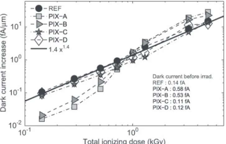
Fig. 8. Radiation-induced dark current linear density increase as a function of total ionizing dose for several pixel layouts.
seems that there is no degradation of the microlens optical properties due toγ-ray irradiation.
Further studies are planed in order to get more information, particularly for short wavelengths, and to get a better knowl-edge on responsivity changes due toγ-radiations.
C. Dark Current
Ionizing radiation is known to induce large dark current rises in CISs. This radiation-induced dark current is usually proportional to the perimeter of the photodiode (see, for ex-ample, [4], [8]). In order to compare the sensor responses, the dark current is expressed here as a dark current linear density per unit of perimeter. Fig. 8 shows the dark current increase as a function of total ionizing dose. The RD sensors have the same photodiode layout as the reference imager but they use different types of transistors in their readout chain. All these RD sensors exhibited the same dark current increase as the reference device, and their response is not shown in the figure for improved clarity. This result was expected since the readout chain MOSFETs are not supposed to play a role in the dark current generation. REF, PIX-C, and PIX-D have similar responses almost proportional to x1.4. Therefore, the use of an ELT in PIX-C and the implantation of a P+guard-ring
Fig. 9. Electrical transfer function degradation measured on sensors RD-C and RD-H. These measurements were performed without double sampling.
increase. It can then be inferred that the reset MOSFET source contribution and interdevice leakages between the collection node and other devices are negligible. As it was concluded at lower total ionizing doses [8], the radiation-induced dark current rise seems only due to an increase of carrier generation at the STI interface, around the photodiode. The extracted dark current activation energy after 5 kGy is 0.631 ± 0.002 eV on the whole pixel population between−20◦C and+23◦C. This value agrees perfectly with the classical value for pure radiation-induced generation current induced by displacement damage or ionization [1], [19], [20] and confirms the previous conclusion. It also shows that this generation current dominates the other contributions, such as MOSFET leakages, interdevice leakages, gate leakages, and tunnel currents.
As it was expected from previous work, RFD photodiodes have a larger dark current before irradiation (see Table II) but they are less sensitive to ionizing radiation than standard CIS diode at low dose. However, above 0.3 kGy, these pixel layouts have a worst dark current increase than the other structures. This behavior suggests that the recessed distanced used is too
short. At low ionizing dose, the depleted region is supposed not to reach the surrounding STI, and the radiation-induced dark current is reduced. At higher dose, the radiation-induced positive trapped charges seem able to extend the depleted region to the STI interface where the interface state and trapped charge densities are much higher. The resulting dark current is then even higher than in the standard photodiode.
D. Readout Chain
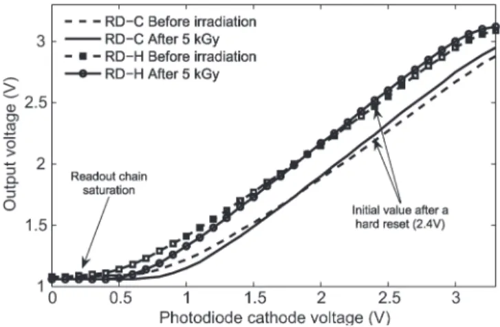
The evolution of the electrical transfer functions Vout(VD)
(see Fig. 1) of devices RD-C and RD-H with irradiation is shown in Fig. 9. After the reset operation, the photodiode cath-ode is biased to 2.4 V in HR mcath-ode.1 Under high illumination
conditions, the photodiode cathode voltageVDcan drop much
leading to the saturation of the readout chain. The resulting output saturation voltage after double sampling is then
Vsat= Vout|VD=2.4 V− Vout|VD=0 V. (4) 1In SR mode, the cathode reaches a voltage slightly higher than theV
D(Soft)
value indicated in Table II.
Fig. 10. Output voltage variation with irradiation for both input voltages: 0 and 2.4 V.
Fig. 10 shows the evolution of Vout|VD=2.4 V and
Vout|VD=0 V. The first voltage increases (between 30 and
65 mV) and the second decreases (between−5 and −30 mV). The corresponding saturation voltage increase after exposure is in fairly good agreement with the variations observed in HR mode in Fig. 4. This result confirms that the degradation of the readout chain is responsible for the saturation voltage increase observed in HR mode.
One can see in Fig. 9 that theVout|VD=2.4 Vrise corresponds
to the change of electrical transfer function slope. Such a change reveals a variation of transconductance and thresh-old voltage, most likely in source followers MOSFETs. The radiation-induced saturation voltage variation vanishes when the in-pixel source follower is edgeless (see PIX-A plot in Fig. 4). Therefore, this effect is supposed to come from the n-channel source follower N1 and the RINCE is once again the most probable cause. Moreover, it means that RINCE seems able to change the source follower N-MOSFET tance. The consequence of RINCE on MOSFET transconduc-tance should be studied in the future to validate this hypothesis. One can also note that a small degradation of the p-channel source follower P1 could possibly explain why a slight satura-tion voltage rise remains at 5 kGy on PIX-A plot in Fig. 4.
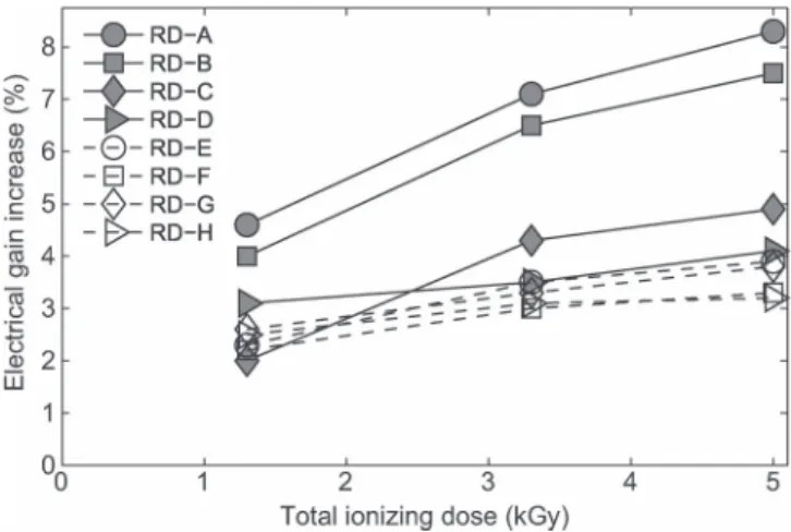
The electrical gain change is plotted as a function of total ionizing dose for all the RD sensors in Fig. 11. This gain is com-puted close to the reset voltage after an SR, forVD≈ VD(Soft).
One can see that this slope slowly rises with irradiation. All the readout chains have a similar behavior except RD-A and RD-B ones. These two devices use only StdVt transistors in their readout chain, resulting in a smaller output voltage swing and a reduced linear region. Therefore, a small threshold voltage shift in these two chains has a larger impact on the linear region and on the electrical gain than in the other devices.
IV. RADIATIONHARDENINGPERSPECTIVES
The image sensor digital part was still fully functional after the maximum ionizing dose, and this part of the circuit does not need any radiation hard design up to 5 kGy. The main ionizing radiation effects observed in the analog part of the tested sensors are the following: a large dark current increase
Fig. 11. Readout chain electrical gain increase with irradiation. The gain is determined from the local slope atVD= VD(Soft).
and a significant saturation voltage increase due to MOSFET threshold voltage shifts (reset transistor and readout chain), subthreshold current increase (reset transistor), and transcon-ductance change (readout chain). The MOSFETs degradations are attributed to the trapped charge in the lateral STI. This charge turns on the lateral parasitic MOSFET on the sides of the active channel, and it induces a threshold voltage shift through the RINCE effect. STIs also seem able to change the narrow MOSFETs transconductance because of its trapped charge or interface states. As regards the change in responsivity, it has to be studied in detail in order to confirm the dominant role of surface recombination.
General radiation hardening guidelines imply the systematic use of edgeless n-channel transistors, such as ELTs, and P+
guard-ring between every N-doped region [21]. The first rule is mainly used to prevent a leakage current to flow between the source and the drain of n-channel MOST while the second is meant to avoid interdevice leakages. It is also interesting to notice that the use of ELT prevents all the STI-related effects, such as RINCE. Interdevice leakage is not a concern in these sensors since the use of P+ guard-ring did not influence the parasitic current on the most sensitive node of the circuit: the photodiode dark current.
Drain-to-source leakage is only a problem in the reset tran-sistor since it contributes to the change in saturation voltage with total ionizing dose, only in SR mode. The use of edgeless MOSFET, such as ELT, eliminates this parasitic current and the RINCE effect. Therefore, the saturation voltage variation due to the exposure toγ-rays can be cancelled. If an ELT is used,
the gate must enclose the reset MOSFET source to prevent the apparition of noticeable radiation-induced dark current in the source junction.
In the readout chain, the RINCE effect on narrowest n-channel and p-channel MOSFETs is supposed to be the main contributor to the degradation. A radiation hardened readout chain can then be achieved by using ELTs or simply by using transistors with large channels. Applying this modification only to the in-pixel source follower MOSFET N2 seems sufficient to ensure good radiation hardness up to 5 kGy. Noticeable RINCE has also been seen on p-channel MOSFET in the same technology [8], and it can become a concern at higher doses or
under different irradiation conditions such as dose rate, biasing, and/or temperature.
Regarding the photodiode dark current, the modification of the surrounding environment of the junction is known to change the photodiode hardness [4], [8] but no universal solution available in this technology exists. The use of a P+implant or a polysilicon gate to isolate the junction from the surrounding STI can be efficient but these solutions are still the object of undergoing studies to find an optimum design. CMOS imaging process which allows the integration of pinned photodiode [22]–[24] can also significantly reduce the dark current increase [7], if the distance between the STI and the junction is well selected. However, radiation effects on the transfer efficiency and on the pinning implant doping density compensation still need further studies.
V. SUMMARY ANDCONCLUSION
An overview of ionizing radiation effects in imagers manu-factured in a 0.18-μm CIS technology was presented. Fourteen
different sensors, with different designs, were irradiated up to 5 kGy and characterized.
After exposure to γ-ray, a wavelength-dependent decrease
in responsivity was also observed on image sensors with and without microlenses. It was shown that an increase of surface recombination velocity due to an increase of interface state density can explain this responsivity drop, particularly at the shortest wavelengths. Moreover, we did not observe a signifi-cant change in microlens optical properties.
Total ionizing dose-induced large saturation voltage shifts and dark current increases. Both effects were attributed to the STIs. The MOSFET gate oxide did not seem degraded by the irradiation and no interdevice leakage was observed. In photodiodes, the defect induced by the irradiation in the surrounding STI enhanced the generation current. In narrow MOSFETs, the lateral STI led to threshold voltage shifts, drain-to-source leakage currents, and a change in transconductance which has to be confirmed by further measurements on iso-lated MOSFETs. The use of low- and zero-threshold-voltage MOSFETs improved slightly the imager radiation hardness. No change was seen in the digital circuit operation after irradiation. In the future, the radiation hardness of this sensor can be easily improved by using edgeless transistors at some key points in the circuit: the in-pixel reset MOSFET and the in-pixel source follower. No interdevice leakage was observed up to 5 kGy. Thus, the integration of P+guard-rings is not supposed
to improve the radiation hardness. Further work is needed to re-duce the radiation-inre-duced dark current by designing a radiation hardened photodiode in this technology. Such a radiation-hard photodiode could then be used in any other commercial CMOS technology.
Considering the relatively small degradations observed and the remaining effort necessary to improve importantly the radiation hardness of image sensor manufactured in deep-submicrometer CMOS imaging technology, these devices seem promising for future space applications and fully compliant with medical imaging requirements. Their compatibility with higher dose environment seems reachable as well.
All these conclusions can be transposed to 4T CISs which share the main part of their architecture with 3T CISs. The ra-diation effects on pinning implant and charge transfer efficiency still need to be further studied.
ACKNOWLEDGMENT
The authors would like to thank F. Corbière for designing the test arrays and P. Cervantes for her important involvement in this paper. The authors would also like to thank P. Malisse and Europractice-IMEC team for their great support and I. Djité for his assistance with measurements.
REFERENCES
[1] G. R. Hopkinson, “Radiation effects in a CMOS active pixel sensor,” IEEE Trans. Nucl. Sci., vol. 47, no. 6, pp. 2480–2484, Dec. 2000. [2] M. Cohen and J.-P. David, “Radiation-induced dark current in CMOS
active pixel sensors,” IEEE Trans. Nucl. Sci., vol. 47, no. 6, pp. 2485– 2491, Dec. 2000.
[3] E.-S. Eid, T. Y. Chan, E. R. Fossum, R. H. Tsai, R. Spagnuolo, J. Deily, W. B. Byers, and J. C. Peden, “Design and characterization of ionizing radiation-tolerant CMOS APS image sensors up to 30 Mrd (Si) total dose,” IEEE Trans. Nucl. Sci., vol. 48, no. 6, pp. 1796–1806, Dec. 2001. [4] B. R. Hancock, T. J. Cunningham, K. P. McCarty, G. Yang, C. J. Wrigley,
P. G. Ringold, R. C. Stirbl, and B. Pain, “Multi-megarad (Si) radiation-tolerant integrated CMOS imager,” Proc. SPIE, vol. 4306, pp. 147–155, 2001.
[5] J. Bogaerts, B. Dierickx, G. Meynants, and D. Uwaerts, “Total dose and displacement damage effects in a radiation-hardened CMOS APS,” IEEE Trans. Electron Devices, vol. 50, no. 1, pp. 84–90, Jan. 2003.
[6] B. Pain, B. R. Hancock, T. J. Cunningham, S. Seshadri, C. Sun, P. Pedadda, C. J. Wrigley, and R. C. Stirbl, “Hardening CMOS im-agers: Radhard-by-design or radhard-by-foundry,” Proc. SPIE, vol. 5167, pp. 101–110, 2004.
[7] P. R. Rao, X. Wang, and A. J. P. Theuwissen, “Degradation of CMOS image sensors in deep-submicron technology due toγ-irradiation,” Solid State Electron., vol. 52, no. 9, pp. 1407–1413, Sep. 2008.
[8] V. Goiffon, P. Magnan, O. Saint-Pé, F. Bernard, and G. Rolland, “Total dose evaluation of deep submicron CMOS imaging technology through elementary device and pixel array behavior analysis,” IEEE Trans. Nucl. Sci., vol. 55, no. 6, pp. 3494–3501, Dec. 2008.
[9] B. Pain, G. Yang, T. J. Cunningham, C. Wrigley, and B. Hancock, “An enhanced-performance CMOS imager with a flushed-reset photodiode pixel,” IEEE Trans. Electron Devices, vol. 50, no. 1, pp. 48–56, Jan. 2003. [10] H. Tian, B. Fowler, and A. El Gamal, “Analysis of temporal noise in CMOS photodiode active pixel sensor,” IEEE J. Solid-State Circuits, vol. 36, no. 1, pp. 92–101, Jan. 2001.
[11] F. Faccio and G. Cervelli, “Radiation-induced edge effects in deep submi-cron CMOS transistors,” IEEE Trans. Nucl. Sci., vol. 52, no. 6, pp. 2413– 2420, Dec. 2005.
[12] H. J. Barnaby, “Total-ionizing-dose effects in modern CMOS technolo-gies,” IEEE Trans. Nucl. Sci., vol. 53, no. 6, pp. 3103–3121, Dec. 2006. [13] T. P. Ma and P. V. Dressendorfer, Ionizing Radiation Effects in MOS
Devices and Circuits. New York: Wiley-Interscience, 1989.
[14] M. R. Shaneyfelt, P. E. Dodd, B. L. Draper, and R. S. Flores, “Challenges in hardening technologies using shallow-trench isolation,” IEEE Trans. Nucl. Sci., vol. 45, no. 6, pp. 2584–2592, Dec. 1998.
[15] G. R. Hopkinson, A. Mohammadzadeh, and R. Harboe-Sorensen, “Radiation effects on a radiation-tolerant CMOS active pixel sensor,” IEEE Trans. Nucl. Sci., vol. 51, no. 5, pp. 2753–2761, Oct. 2004. [16] M. Fernandez-Rodriguez, C. G. Alvarado, A. Nunez, and A.
Alvarez-Herrero, “Modeling of absorption induced by space radiation on glass: A two-variable function depending on radiation dose and post-irradiation time,” IEEE Trans. Nucl. Sci., vol. 53, no. 4, pp. 2367–2375, Aug. 2006. [17] C.-S. S. Lin, B. P. Mathur, and M.-C. F. Chang, “Analytical charge
collec-tion and MTF model for photodiode-based CMOS imagers,” IEEE Trans. Electron Devices, vol. 49, no. 5, pp. 754–761, May 2002.
[18] F. Van de Wiele, “Photodiode quantum efficiency,” in Solid State Imaging. Leyden, The Netherlands: Noordhoof Int. Publishing, 1976, pp. 47–90. [19] J. R. Srour, S. C. Chen, S. Othmer, and R. A. Hartmann, “Neutron
damage mechanisms in charge transfer devices,” IEEE Trans. Nucl. Sci., vol. NS-25, no. 6, pp. 1251–1260, Dec. 1978.
[20] J. R. Srour and D. H. Lo, “Universal damage factor for radiation induced dark current in silicon devices,” IEEE Trans. Nucl. Sci., vol. 47, no. 6, pp. 2451–2459, Dec. 2000.
[21] H. L. Hughes and J. M. Benedetto, “Radiation effects and hardening of MOS technology: Devices and circuits,” IEEE Trans. Nucl. Sci., vol. 50, no. 3, pp. 500–521, Jun. 2003.
[22] N. Teranishi, A. Kohno, Y. Ishihara, E. Oda, and K. Arai, “An inter-line CCD image sensor with reduced image lag,” IEEE Trans. Electron Devices, vol. ED-31, no. 12, pp. 1829–1833, Dec. 1984.
[23] B. C. Burkey, W. C. Chang, J. Littlehale, T. H. Lee, T. J. Tredwell, J. P. Lavine, and E. A. Trabka, “The pinned photodiode for an interline-transfer CCD image sensor,” in IEDM Tech. Dig., 1984, pp. 28–31. [24] T. Lule, S. Benthien, H. Keller, F. Mutze, P. Rieve, K. Seibel, M. Sommer,
and M. Bohm, “Sensitivity of CMOS based imagers and scaling perspec-tives,” IEEE Trans. Electron Devices, vol. 47, no. 11, pp. 2110–2122, Nov. 2000.
Vincent Goiffon (S’08–M’09) was born in Toulouse, France, in 1980. He received the M.S. degrees in electrical engineering and aeronautics and astronautics from Ecole Nationale Supérieure de l’Aéronautique et de l’Espace, Toulouse, in 2005 and the Ph.D. degree in electrical engineering from the Université de Toulouse, Toulouse, in 2008. His doctoral research, partly funded by CNES and EADS Astrium, focused on space radiation effects on deep-submicrometer CMOS sensors and hardening-by-design techniques.
Since 2008, he has been an Assistant Professor with the Image Sensor Laboratory, Institut Supérieur de l’Aéronautique et de l’Espace, Université de Toulouse. His research interests include solid-state image sensors, integrated circuit design, device TCAD modeling and simulation, semiconductor defect characterization, ionization and displacement damage effects, and random telegraph signal in pixel arrays.
Magali Estribeau was born in Toulouse, France,
in 1976. She received the M.S. and Ph.D. de-grees in electrical engineering from Ecole Na-tionale Supérieure de l’Aéronautique et de l’Espace, Toulouse, in 2000 and 2004, respectively. Her Ph.D. work, partly funded by EADS Astrium, focused on the study and the modeling of the CMOS imager Modulation Transfer Function.
She is currently a Research Scientist with the Image Sensor Laboratory, Institut Supérieur de l’Aéronautique et de l’Espace, Université de Toulouse, Toulouse. Her research interests include solid-state image sensors, electrooptical performances characterization methods, sensitivity analysis and enhancement, and image quality.
Pierre Magnan (M’99) was born in Nevers, France,
in 1958. He received the M.S. and D.E.A. degrees in integrated circuit design from the University of Paris XI, Orsay, France, in 1982 and the Agrégation degree in electrical engineering from Ecole Normale Supérieure de Cachan, Cachan, France.
From 1984 to 1993, he was involved in CMOS analog and semicustom design with LAAS-CNRS Laboratory, Toulouse, France. In 1995, he joined the CMOS Imagers Research Group, Ecole Na-tionale Supérieure de l’Aéronautique et de l’Espace (SUPAERO), Toulouse, where he was involved in active-pixel sensor research and development activities. In 2002, he got his Accreditation for Ph.D. Super-vision (H.D.R.) and became Full Professor with SUPAERO, currently called Institut Supérieur de l’Aéronautique et de l’Espace, Université de Toulouse, Toulouse, where he is currently Head of CMOS Imagers Research Group. He has been supervising eight Ph.D. candidates in the field of image sensors and has authored or coauthored 30 papers and a patent. His research interests include solid-state image sensors design, modeling, and technology, and inte-grated circuit design for imaging applications.
Prof. Magnan has been a member of the program committee of the Interna-tional Image Sensor Workshop in 2007 and 2009.