Si1-xGex growth using Si3H8 by low temperature chemical vapor deposition
Shotaro Takeuchi a·b·c·, Ngoc Duy Nguyen a, Jozefien Goosens a, Matty Caymax a, Roger Looa a IMEC, Kapeldreef 75, B-3001 Leuven, Belgium
b Department of Physics and Astronomy, Katholieke Universiteit Leuven, Celestijnenlaan 200D, B-3001 Leuven, Belgium
c Department of Crystalline Materials Science, Graduate School of Engineering, Nagoya University, Furo-cho,
Chikusa-ku, Nagoya 4β4-8β03, Japan
Keywords: Si1-xGex ; Si3H8;Low temperature; chemical vapor deposition; CMOS;BiCMOS
ABSTRACT: Low temperature epitaxial growth of group-IV alloys is a key process step to realize the advanced Si-based devices. In order to keep high growth rate below 600 °C, trisilane (Si3H8) was used for their growth as an alternative Si precursor gas. Then, we compared the use of Si3H8 versus SiH4 for Si1-xGex growth in H2 and N2 as carrier gas by low temperature chemical vapor deposition. By using Si3H8 and controlling GeH4 flow rate, Si1-xGex growth with high growth rate and wide range of Ge concentration has been achieved compared to SiH4-based process. The growth rate and Ge concentration in Si1-xGex with Si3H8 grown at 600 °C ranged from 11 to 74nm/min and from 0 to 40%, respectively. The obtained growth rates with Si3H8 are between 1.5 and 6 times higher than for SiH4 at a given growth condition. Si3H8-based in-situ B- and C-doped Si1-xGex growth with high growth rate was also demonstrated.
1. Introduction
Low-temperature epitaxial growth of group-IV alloys is a key process step for the achievement of advanced Si-based (bipolar) complementary metal-oxide-semiconductor (CMOS, BiCMOS) applications. This process is now used in embedded and raised source/ drains with strained Si1-xGex and strained Si1-yCy for CMOS and fully-strained base layer of Si1-xGex and Si1-x-yGexCy for BiCMOS [1-4], Because these Si-based group-IV layers are highly doped and fully-strained, low thermal budget is required to avoid any undesirable dopant diffusion and strain relaxation. For example, it is required to limit the doping diffusion in the existing CMOS devices for BiCMOS applications. Obviously, the thermal budget during epi processing is defined by both the pre-epi bake, used to remove traces of oxide and carbon after the last wet-chemical treatment, as well as the growth
temperature during epitaxial growth. Several groups (among which IMEC) studied the impact of the pre-epi treatments on substrate/epi interface contamination and its importance for device performance, see for example reference [5,6]. Effort is ongoing to reduce the pre-epi bake temperature to temperatures ≤ the growth
temperature. In the classical chemical vapor deposition (CVD) approach, Si-based epitaxial layers were grown by mainly using SiH4 or SiCl2H2 as Si precursor gas. A reduction of the growth temperature leads to a large reduction of the growth rate, which means that sustaining a high throughput becomes very difficult. There are two routes to enhance growth rates: one is the use of N2 as carrier gas instead of H2 [7]. Another one is the use of high order silane precursor gases such as trisilane (Si3H8) [8-10]. High growth rates at growth temperatures below 600 °C for both routes have been demonstrated. However, the growth behavior has not been fully clarified. In this work, we demonstrate Si1-xGex growth using Si3H8 (commercially developed by Voltaix as Silcore®) and SiH4 as Si precursor gases and using either H2 or N2 as carrier gas. We will describe the
differences of the growth kinetics and behavior for both Si precursor gases and both carrier gases. The success of the developed Si1-xGex process will be illustrated by full Si/SiGe:C base layers which also contain a B doping spike as used in BiCMOS technology. The same layer quality as a conventional process has been achieved but the higher growth rate enables a strong reduction of thermal budget.
2. Experimental
Epitaxial Si1-xGex layer growth was performed in an ASM Epsilon™ 2000 reactor which is a horizontal cold wall, load-locked reduced pressure CVD system. Si1-xGex layer growth between 500 °C and 600 °C was done on 200 mm wafers using GeH4, (1% diluted in H2) as Ge precursor gas and the above-mentioned Si precursor gases. B- and C-doped Si1-xGex layer was also grown at 600 °C using 50 ppm B2H6 and 1% CH3SiH3 diluted in H2 as B and C source gas, respectively. The focus of this work lies on a reduction of the thermal budget during epitaxial layer growth. Therefore, we used a conventional wet clean and a 2 min pre-epi bake at 1050 °C to remove the native oxide before growth. As mentioned above, the reduction of pre-epi bake temperature is also important and described in [6]. Scanning electron microscopy (SEM) and spectroscopic ellipsometry (SE) were used to measure the Si1-xGex thickness. SE also allows us to extract the Ge concentration. The Si1-xGex surface morphology was inspected by a Nomarski optical microscope and SEM. In order to estimate the crystalline quality of the Si1-xGex layers, photoluminescence (PL) and secondary ion mass spectrometry (SIMS) were used. We also used SIMS to measure the chemical B concentration in our Si1-xGex layers. The resistivity of B-doped Si1-xGex epilayer was calculated by using a classical four-point-probe method combined with the thickness measurement by SE. From this result, the carrier concentration in the epilayer could be estimated from well-known carrier mobility data of Si. As a consequence, our calculated carrier concentration could be overestimated
because the carrier mobility of Si1-xGex in low Ge content region is degraded due to the alloy scattering compared to the carrier mobility of Si [11].
3. Results and discussion
3.1. Crystalline quality ofSi1-xGex using Si3H8
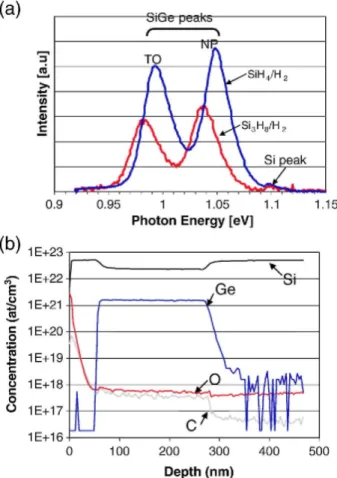
Since Si3H8 is a liquid source at room temperature, one of the concerns for the growth of Si1-x Gex using Si3H8 is the impurity level in the Si1-xGex layer. Therefore, we first examine the crystalline quality by PL and carbon (C) and oxygen (0) levels in the Si1-xGex layer by SIMS. Fig. 1(a) shows the PL spectra of layer stacks consisting Si-cap (50 nm)/ Si1-xGex (200 nm)/Si(00l) and using SiH4/H2 and Si3H8/H2 processes, respectively. Despite of the lower intensity of Si1-xGex with Si3H8 compared to the SiH4 case, high intensity, well-resolved no-phonon (NP) transition and transverse optical (TO) replica from Si1-xGex layer using Si3H8 were observed. This illustrates a low defect level and the absence of non-radiative recombination center in the sample. The slightly higher Ge content as confirmed by SE explains the shift of the PL peaks to lower energies for the sample grown with Si3H8/ H2 process. Fig. 1(b) shows the SIMS profile of the same layer stack with Si3H8 as shown in Fig. 1 (a). The C and O level in the Si1-xGex layer are below 1 E1 8 at/cm3. This impurity level is similar to that of SiH4-based process. These results indicate good crystalline and interface quality of Si1-xGex grown with Si3H8.
Fig. 1. (a) PL spectra measured at 77 K of Si-cap (50nm)/ Si1-xGex (200nm)/Si(001). The Si1-xGex was grown
using either SiH4 or Si3H8 while the Si-cap was, in both cases, grown with Si3H8. The Ge concentrations were
14% for the use of SiH4 and 16% for the use of Si3Hs, respectively, as obtained by SE. (b) SIMS profiles of the
same sample with Si3H8 as shown in Fig. 1 (a). After the well-known surface peaks caused, the C and 0 levels in
the Si1_xGex layer are at the SIMS background levels similar to the SIMS results as obtained for Si1_xGex layer
grown with SiH4/GeH4.
3.2. Comparison of Si1-xGex growth kinetics with different Si precursor gas and carrier gas
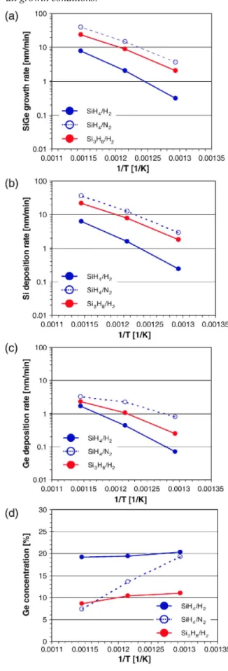
In the next step, we investigated on the differences between, on the one hand, Si3H8 and SiH4 as Si precursor gas, and, on the other hand, between H2 and N2 as carrier gas, regarding the growth behaviors for Si and Si1-xGex. In order to perform a fair comparison, the amount of Si atoms injected into the epi reactor is the same for all Si1-xGex growth conditions in this section. Fig. 2's subpanels (a),(b), (c), and (d) show, respectively, the total Si1-xGex growth rates, the Si component deposition rates, the Ge component deposition rates, and the Ge concentrations using SiH4/H2, SiH4/N2, and Si3H8/H2 processes as a function of the reciprocal temperature. The use of N2 as a carrier gas or Si3H8/H2 results in a higher growth rate compared to the standard SiH4/H2 process (Fig. 2(a)). Generally, at low growth temperature, i.e. below 600 °C, the growth rate is controlled by the presence
of H on the growing surface. This H passivation comes from the precursor gases and from the H2 carrier gas. The low H partial pressure in the SiH4/N2 case results then in a higher Si component deposition rate than SiH4/H2 case [7]. On the other hand, in the Si3H8/H2 case, although H2 is used as carrier gas, the Si component deposition rate is much higher than for the SiH4/H2 case even at 500 °C (Fig. 2(b)). This means that the adsorption
mechanism of Si3H8 is different from that of SiH4 as discussed in the next paragraph. As shown in Fig. 2(c), the Ge incorporation seems to be in the transition region from kinetic to transport regime, especially for the SiH4/N2 process. This explains the strong temperature dependence of the Ge content as obtained for the SiH4/N2 process (Fig. 2(d)).
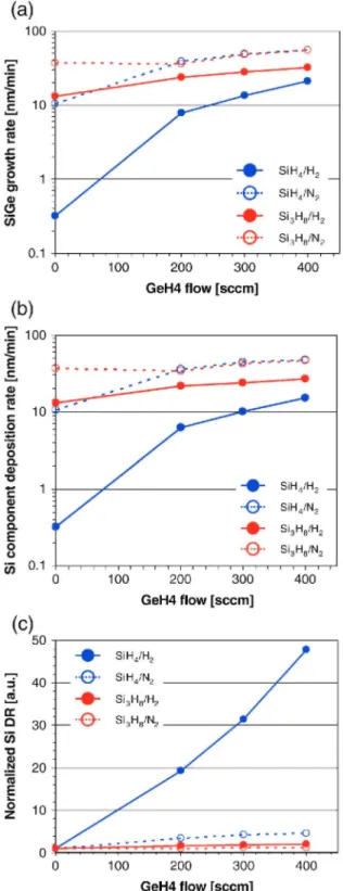
Fig. 3(a) and (b) shows Si1-xGex growth rates and Si component deposition rates in the Si1-xGex layer as a function of GeH4 flow rate, respectively. The growth temperature is fixed at 600 °C Again, the amount of Si atoms injected into the reactor is the same for all Si1-xGex growth conditions. For pure Si growth in H2 (GeH4-flow = 0sccm), we obtained higher Si growth rate for Si3H8 than for SiH4. On the other hand, if we use N2 as carrier gas and GeH4 flows above 200 sccm, similar Si1-xGex growth rates and Si component deposition rates in the layer are obtained for both Si precursors. Fig. 3(c) shows the normalized Si component deposition rate as function of GeH4 flow. This rate is defined as [Si component deposition rate in the Si1-xGex layer]/[pure Si growth rate without GeH4 flow].
The enhancement of the Si component deposition rate by adding GeH4 called "Ge catalytic effect" [12] is clearly seen in Si1-xGex growth using SiH4 in H2. However, for the other three cases, the effect is relatively weak, especially in the case of Si1-xGex growth using Si3H8. This is explained by the fact that the Si deposition in the Si1-xGex layer using Si3H8 is not limited by hydrogen desorption from the growing surface [14-16]. This can also explain why the Si deposition rate is much higher than for the SiH4/H2 case, even at 500 °C A possible
explanation for this behavior is that Si3H8 can react with a Si-H bound or Si- on the surface forming a four-center bound transition state, due to the nuclephilic character of the Si2H5 group, resulting in an "exchange of ligands" with the Si surface (Fig. 4)[14-16]. These Si hydrides with high reactivity decompose to form Si via a facile hydrogen desorption and result in an enhanced Si1-xGex growth rate [13-16]. Similar growth rates are obtained for SiH4/N2 and Si3H8/N2 processes (Fig. 3(a)). However, these processes results in defective epilayers, which is not the cases for SiH4/H2 and Si3H8/H2 processes.
This growth process needs to be optimized to avoid the generation of defects, which is beyond the scope of this paper.
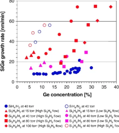
Fig. 5 shows Si1-xGex growth rates using Si3H8 and SiH4 in H2 and N2 as a function of Ge concentration under various growth conditions. The growth rate and the Ge concentration with the SiH4/H2 process at 40 Torr range from 0.3 to 21 nm/min and from 0 to 30%, respectively. The incorporation efficiency limits the Ge concentration in the Si1-xGex layer for the Si3H8 process. However, it can be solved by an optimization of the process
conditions. As shown in Fig. 5, the Si3H8/H2 process provides a high growth rate and a wide variation of Ge concentration in the layer ranging from 11 to 74 nm/min and from 0 to 40% Ge, respectively. For a given Ge concentration in Si1-xGex layer, the use of Si3H8/H2 yields between 1.5 and 6 times higher growth rate than that of SiH4/H2.
Fig. 2. (a) Si1-xGex growth rates, (b) Si component deposition rates in the Si1-xGex layer, (c) Ge component
deposition rates in the Si1-xGex layer, and (d) Ge concentration using SiH4/H2 (blue solid line), SiH4/N2 (blue
dotted line), and Si3Hs/H2 (redsolid line) processes as functions of the reciprocal temperature. Si1-xGex growth
temperatures are 500 °C, 550 °C, and 600 °C. The amount of Si atoms injected into the reactor is the same for all growth conditions.
Fig. 3. (a) Si1-xGex growth rates, (b) Si component deposition rate in Si1-xGex layers, and (c) normalized Si
component deposition rates using SiH4/H2 (blue solid line), SH4/N2 (blue dotted line), Si3Hs/H2 (red solid line),
and Si3Hs/N2 (red dotted line) processes as functions of the GeH4 flow. Si1-xGex growth temperature is fixed at
600 °C The amount of Si atoms injected into the reactor is the same for all growth conditions.
Fig. 4. Schematic diagrams of a Si3H8 dissociation step on a Si site (a) without H passivation, and (b) with H
passivation. In both cases, high reactive Si hydrides are generated, leading to an enhancement of the growth rates.
Fig. 5. Si1-xGex growth rates as a function of Ge concentration in the layers. Filled blue circles: SiH4/H2 process,
open blue circles: SiH4/N2 process, open red circles: Si3H8/N2 process, Si1-xGex layers are grown at 600 °C and
40 Torr. For Si3Hs/H2 process, filled red and pink symbols indicate high and low Si3Hs flow rate. Triangles: 15
Torr, circles: 40Torr, squares: 80Torr, and diamond: 100Torr.
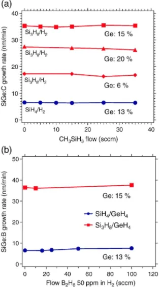
Fig. 6. Si1_xGex growth rates using Si3Hs/H2 process with (a) C and (b) B doping, respectively. For comparison,
the data of SiH4/H2 process was also shown. All Si1-xGex layers were grown at 600 °C and 40Torr. For (a), blue
symbols show SiH4/H2 process (Ge: 13%). Others show Si3H8/H2 processes with high Si3H8 and GeH4 flows
(square) (Ge: 15%), low Si3H8 and high GeH4 flows (triangle) (Ge: 20%), and high Si3H8 and low GeH4 flows
(diamond) (Ge: 6%). For (b), blue symbols show SiH4/H2 process (Ge: 13%), and red ones show high Si3H8 and
GeH4 flows (Ge: 15%).
3.3. Boron- and carbon-doped Si1-xGex growth using Si3H8/H2 process
We have also demonstrated in-situ C- and B-doped Si1-xGex growth using Si3H8/H2 process for SiGe-based BiCMOS applications. Fig. 6(a) and (b) shows Si1-xGex growth rates using Si3H8/H2 process with B and C doping, respectively. For comparison, the data of SiH4/H2 process was also shown in Fig. 6. No significant impact of doping on growth rate in both doping cases was observed. For a similar Ge concentration, the use of Si3H8/H2 gives 5 times higher growth rate than that of SiH4/H2. As shown in Fig. 7(a), total and active B
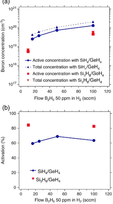
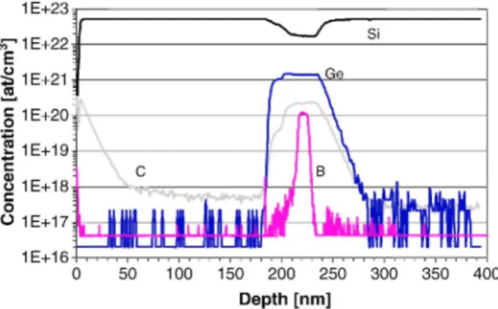
concentration in both Si precursor gas cases increase with increasing effective B2H6 flow ranging from 10 to 100 seem. It should noted that the B dopant activation in the Sio.85Ge0.15 layer using the Si3H8/H2 process is 34% higher than that with the SiH4/H2 process as shown in Fig. 7(b). This result indicates that the formation of electrically inactive B clusters can be avoided because the Si3H8/H2 process is low thermal budget. Fig. 8 shows a SIMS profile of preliminary fabricated HBT base stacks using Si3H8/H2 process, which includes a B dopant spike and a two-step Ge profile with C doping to reduce B diffusion. The B dopant spike layer with high B concentration of 1E20 at/cm3 is well confined between C-doped Si0.8Ge0.2 layers.
4. Conclusions
We have demonstrated Si1-xGex growth using Si3H8 as Si precursor gas and described the growth behavior. The Si1-xGex growth using Si3H8/H2 is a very efficient process with high crystalline layer quality and a high growth rate up to 74 nm/min. The obtained growth rates with Si3H8/H2 are between 1.5 and 6 times higher than for SiH4/
H2 at a given growth condition. Our Si3H8-based Si1-xGex process scheme leads to an improvement of the throughput and a reduction of the thermal budget, which is important especially for advanced BiCMOS
applications. For advanced SiGe-based CMOS applications, high Ge concentrations are needed. At the moment, we can reach Ge concentration up to 40% with our Si3H8-based Si1-xGex process. However, we expect that higher Ge concentrations are achievable by further optimization of the epitaxial growth conditions. This future
investigation is a natural extension of the present work.
Fig. 7. (a) Total and active B concentrations in Sio.s5Geo.15 layer using Si3H8/H2 process and (b) ratio of the
active B concentration over the total B concentration as a function of the effective B2H6 flow. For comparison,
the data obtained for the SiH4/H2 process are also shown. Red and blue symbols indicate Si3H8/H2 and SiH4/H2
processes, respectively.
Fig. 8. Preliminary SIMS profiles of a preliminary fabricated HBT base stack using the Si3H8/H2 process, which
includes a B dopant spike and a two-step Ge profile with C doping to reduce B diffusion. B depth profile was measured by O+ beam with a beam energy of 500 eV. Si, Ge, and C depth profiles were measured by Cs+ beam
with a beam energy of 5 keV. The C background level can be observed from about 50 nm, after the surface peak.
Acknowledgement
The supply of Silcore® by Voltaix, Inc. is gratefully acknowledged. The authors wish to thank Matthew Stephens and Michael Pikulin from Voltaix for helpful discussions. Fruitful discussion with Rick Wise (Texas Instruments) is gratefully acknowledged.
References
[1] Y.C. Yeo, Semicond. Sci. Technol. 22 (2007) SI 117.
[2] P. Verheyen, G. Eneman, R Rooyackers, R Loo, L. Eeckout, D. Rondas, F. Leys, J. Snow, D. Shamiryan, M. Demand, T.H.Y. Hoffmann, M. Goodwin, H. Fujimoto, C. Ravit, B.-C Lee, M. Caymax, K. De Meyer, P. Absil, M. Jurczalk, S. Biesemans, IEDM, technical digest, 2005, p. 907.
[3] P. Verheyen, V. Machkaoutsan, M. Bauer, D. Weeks, C. Kerner, F. Clemente, H. Bender, D. Shamiryan, R Loo, T. Hoffmann, P. Absil, S. Biesemans, S.G. Thomas, IEEE Electron Device Lett. 29 (2008) 1206.
[4] LJ. Choi, A. Sibaja-Hernandez, R Venegas, S. Van Huylenbroeclk, S. Decoutere, IEEE Trans. Electron Devices 55 (2008) 358. [5] Y. Shimamune, M. Fukuda, M. Koiizuka, A Katakami, A Hatada, K. Ikeda, Y Kim, K. Kawamura, N. Tamura, T. Mori, A Moriya, Y Hashiba, Y. Inokuchi, Y Kunii, M. Kase, VLSI Tech. Dig. 116(2007).
[6] R Loo, A Hikavyy, F. Leys, M. Wada, K. Sano, B. De Vos, A. Pacco, M. Bargallo Gonzalez, E. Simoen, P. Verheyen, W. Vangerle, M. Caymax, Solid State Phenomena 145-146 (2009) 177.
[7] P. Meunier-Beillard, M. Caymax, K.V. Nieuwenhuysen, G. Doumen, B. Brijs, M. Hopstaken, L Geenen, W. Vandervorst, Appl. Surf. Sci. 224 (2004) 31.
[8] M.A Todd, K.D. Weeks, Appl. Surf. Sci. 224 (2004) 41.
[9] A Gouyé, O. Kermarrec, Y Campidelli, P. Bajolet, P. Tomasini, S.G. Thomas, T. Billon, D. Bensahel, Abstracts of Int. Conf. Silicon
Epitaxy and Heterostructures, 2007, p. 204.
[10] N.D. Nguyen, R Loo, M. Caymax, Appl. Surf. Sci. 254 (2008) 6072. [11] M.V. Fischetti, S.E. Laux, J. Appl. Phys. 80 (1996) 2234.
[12] P.M. Garone, J.C. Sturm, P.V. Schwartz, S.A Schwarz, B.J. Wilkens, Appl. Phys. Lett. 56 (1990) 1275. [13] S.M. Gates, Surf. Sci. 195 (1988) 307.
[14] M. Stephens, Voltaix, U.S.A, private commun, Apr. 22, 2008. [15] J.J. Watlkins, M.D. Sefcik, M.A. Rind, Inorg. Chem. 11 (1972) 3147.
[16] M. Caymax, F. Leys, J. Mitard, K. Martens, L Yang, G. Pourtois, W. Vandervorst, M. Meuris, and R Loo, submitted to I. Electrochem.
Soc.