Publisher’s version / Version de l'éditeur:
Lab on a chip, 6, 7, pp. 936-941, 2006-04-21
READ THESE TERMS AND CONDITIONS CAREFULLY BEFORE USING THIS WEBSITE. https://nrc-publications.canada.ca/eng/copyright
Vous avez des questions? Nous pouvons vous aider. Pour communiquer directement avec un auteur, consultez la première page de la revue dans laquelle son article a été publié afin de trouver ses coordonnées. Si vous n’arrivez pas à les repérer, communiquez avec nous à PublicationsArchive-ArchivesPublications@nrc-cnrc.gc.ca.
Questions? Contact the NRC Publications Archive team at
PublicationsArchive-ArchivesPublications@nrc-cnrc.gc.ca. If you wish to email the authors directly, please see the first page of the publication for their contact information.
NRC Publications Archive
Archives des publications du CNRC
This publication could be one of several versions: author’s original, accepted manuscript or the publisher’s version. / La version de cette publication peut être l’une des suivantes : la version prépublication de l’auteur, la version acceptée du manuscrit ou la version de l’éditeur.
For the publisher’s version, please access the DOI link below./ Pour consulter la version de l’éditeur, utilisez le lien DOI ci-dessous.
https://doi.org/10.1039/b600584e
Access and use of this website and the material on it are subject to the Terms and Conditions set forth at
High fidelity, high yield production of microfluidic devices by hot
embossing lithography : Rheology and stiction
Cameron, Neil S.; Roberge, Helene; Veres, Teodor; Jakeway, Stephen C.;
Crabtree, H. John
https://publications-cnrc.canada.ca/fra/droits
L’accès à ce site Web et l’utilisation de son contenu sont assujettis aux conditions présentées dans le site LISEZ CES CONDITIONS ATTENTIVEMENT AVANT D’UTILISER CE SITE WEB.
NRC Publications Record / Notice d'Archives des publications de CNRC:
https://nrc-publications.canada.ca/eng/view/object/?id=00b6b34d-77c7-4908-9e3c-d6462590050e
https://publications-cnrc.canada.ca/fra/voir/objet/?id=00b6b34d-77c7-4908-9e3c-d6462590050e
High fidelity, high yield production of microfluidic devices by hot embossing
lithography: rheology and stiction
Neil S. Cameron,*
aHelene Roberge,
aTeodor Veres,
aStephen C. Jakeway
band H. John Crabtree
bReceived 17th January 2006, Accepted 21st April 2006
First published as an Advance Article on the web 16th May 2006 DOI: 10.1039/b600584e
We discuss thermoforming of thermoplastic polymers for the hot-embossing lithographic (HEL) fabrication of microfluidic chips near equilibrium conditions that minimize elastic recoil for optimal motif replication. While HEL is often simplistically described as the transfer of micro- and nano-motifs into heat-softened thermoplastic materials, we describe our rational approach to selecting appropriate processing parameters.
Introduction
The increasing demand for polymer-based devices as well as for low-cost micro- and nano-fabrication technologies requires the development of reproducible protocols for manufacturing using inexpensive materials. Replication of micro- and nanostructures with polymers is an active area of research, often employing injection moulding and hot embossing.1 A good example of the utility of hot embossing is in the fabrication of chips for micro total analysis systems (mTAS), where flow channels, reservoirs and mixing chambers can be designed and fabricated directly in a single-layer polymer chip. The micro electromechanical systems (MEMS) research community has recently adopted these technologies for the replication of precision plastic/metallic microstructures, and to develop low cost mass-production-compatible microfabrica-tion techniques for the commercializamicrofabrica-tion of MEMS devices.2 Many thermoplastic polymers have been investigated as candidate materials for such applications, including poly-(methyl methacrylate) (PMMA), poly(cyclic olefin) (PCO or COC), polycarbonate (PC), poly(tetrafluoroethylene) (PTFE), polystyrene (PS) and others (Table 1).3–5
Polymer hot embossing is an attractive alternative for the replication of micro and sub-micro features in thermoplastic materials with dimensions from a few nanometres to several centimetres.6,7 Motifs include vias, cruciform electrophoretic channels, mixing chambers, serpentine races and retention posts. Standard micro- and nano-fabrication techniques are employed to generate stamps. The resulting devices are characterized by SEM as well as contact and/or optical profilometry.
HEL and the glass transition
It is convenient, though deceptively simple, to describe the embossing process as the transfer of motifs into a polymer film heated above its glass transition temperature (Tg).
Nevertheless, once transfer has been accomplished, the stamp and the film are separated and post-embossing processing releases functional devices. Careful stamp design6 and
judicious application of release agents8 are necessary for successful motif replication, but the embossing process itself is rich in rheological and interfacial phenomena. Choosing appropriate processing parameters is therefore critical for high fidelity and high yield production of bioMEMS by HEL.
Displacing polymers in thin films is often treated purely in terms of Tg, viscocity and the characteristic relaxation time, t.
9
In fact, these parameters are somewhat complicated and among the first operational parameters to be determined is an optimal embossing temperature. Visco-elastic systems do not behave as classical Newtonian fluids at or near the glass transition. A purely elastic response obeys Hooke’s law where the reversible displacement is a function of force and the spring constant. A purely viscous response, on the other hand, is described by Newton’s law where the stress equals the shear rate corrected by the viscocity of the material. Canonical bulk
a
Industrial Materials Institute: National Research Council Canada, 75 Blvd. De Mortagne, Boucherville, Que´bec, J4B 6Y4, Canada. E-mail: neil.cameron@cnrc.gc.ca; Fax: +1 (450) 641-5105; Tel: +1 (450) 641-5168
bMicralyne Inc., 1911-94 Street, Edmonton, Alberta, T6N 1E6, Canada.
E-mail: sjakeway@micralyne.com; Fax: +1 (780) 431-4422; Tel: +1 (780) 431-4419
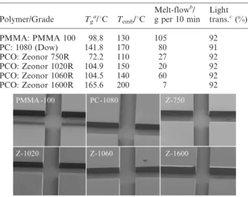
Table 1 Selected polymer properties and embossed structures (50 mm channel width)
Polymer/Grade Tga/uC Temb/uC
Melt-flowb/ g per 10 min Light trans.c(%) PMMA: PMMA 100 98.8 130 105 92 PC: 1080 (Dow) 141.8 170 80 91 PCO: Zeonor 750R 72.2 110 27 92 PCO: Zeonor 1020R 104.9 150 20 92 PCO: Zeonor 1060R 104.5 140 60 92 PCO: Zeonor 1600R 165.6 200 7 92 aTA-Q1000 DSC at 20
uC min21. bVarious standards. c
Commercial values.
and thin-film thermoplastic polymers are neither perfectly elastic nor perfectly viscous due to their chain-like structure. For any given polymer, each response is attenuated by the other to varying degrees, depending largely on the temperature of the system.10 Above the glass transition temperature, significant segmental motion of the polymer chains renders possible a viscous response to an applied stress. Thermoplastic polymers undergo three regime transitions as they are heated from the glassy state below the Tg, through the leathery phase
during the Tgtransition, to a visco-elastic rubbery plateau until
sufficient energy is supplied and the elastic response is completely dominated by viscous flow. The temperature range of the rubbery plateau is polymer and chain-length dependent. Clearly, the optimal embossing temperature is above Tgat the
cusp of the viscous regime, where the relaxation time of the polymer, t, is exceedingly fast and where residual stresses caused by the thermoforming of the polymer will be minimized in the absence of a rapid ‘quenched’ cooling step.11,12 Arbitrary embossing values such as Temb= (Tg+ n) uC (where
n is a universal integer) are most unlikely to provide optimal
embossing conditions.
Careful optimization of the process parameters, especially the embossing temperature (Temb), is required to avoid
damaging the embossing stack, as well as to avoid trapping residual stress and subsequent rebound,13 and also to avoid unduly long cycle times caused by excessive heating and cooling. Choosing by how much the embossing temperature should exceed the Tgis a compromise between the reduction in
the polymer moduli that facilitate faithful motif replication and the potential damage to stamp and substrate caused by longer cycle times and greater thermal distortion.
Hot embossing process
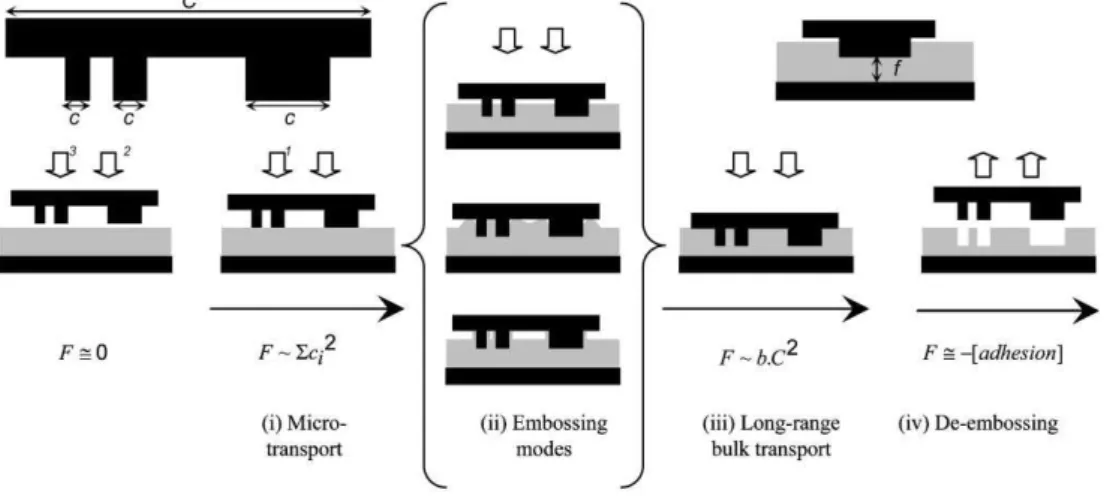
The embossing process is shown schematically in Fig. 1. Initially, a textured stamp is pressed into a heat softened polymer, and the force required for the micro-transport of
displaced polymer scales with the contact area of the stamp features with the polymer (Fig. 1-i). As the stamp progresses into the substrate, the material displacement may, in principle, be purely viscous or elastic. In practice, however, the response is usually both (Fig. 1-ii, middle). Various idealized represen-tations of the filling mechanism have been presented,9,14
however most agree that once the stamp cavities are filled, then the embossing force scales with the entire contact area with a correction factor for the long-range transport of polymer to the edge of the stamp (Fig. 1-iii). Elucidating the details of the embossing process is not trivial, especially in the nano-regime, and instrumented approaches such as one-dimensional surface probe microscopy8 and indentation are useful techniques to
explore the development of micro- and nano-motifs.15 The most complicated regime occurs when the residual film thickness between the stamp motifs and the support under-layer approaches the polymer coil dimension. Polymers physisorb to silicon and silicon oxide surfaces as a function of the interfacial interaction. In the case of PMMA on a SiO2
surface, dipole–dipole and H-bonding interactions effectively tether the polymer to the surface. The polymer conformation in this state may be described as the sum of trains (chains ‘lying’ on the surface), loops (segments between trains) and tails (loose ends).16We and others have observed an important increase in Tg at this interface for this system. Where the
interaction is not favourable, for example when a non-polar polymer is coated on native SiO2 on a silicon wafer, the
polymer conformation tends to favour loops, with the concomitant increase in free-volume and subsequent decrease in apparent Tg.17–24 This phenomenon has been explored for
thermomechanical data storage in polymer thin-films.25 The final, and often most challenging, phase of the embossing cycle is the separation of stamp and substrate, since the two have been pressed together at elevated tempera-tures and forces in evacuated chambers to assure conformality. Anti-stiction agents such as the hydroperfluorosilanes are
Fig. 1 The total force required to emboss a thermoplastic polymer (F) depends on the polymer’s viscosity, volume to be displaced, film thickness and temperature. When positive motifs are brought into contact with the polymer above Tg, F scales with the contact area (i). The transitional
mechanism (ii) sits in the spectrum of visco-elastic behaviour (observed mechanism, ii-middle; idealized schematics, ii-upper and ii-lower) and the annealing period for successful HEL must account for the polymer relaxation time, t. When the stamp is fully embossed (i.e. no further short-range transport is possible), the force required to effect long-range displacement of the polymer scales with the surface area of the entire stamp (C2) with a
correction for the long-range bulk transport of polymer chains (iii). For supported thin films, F becomes very high as the residual thickness, f, approaches values below the radius of gyration of the polymer chains (iii). De-embossing occurs when the force of adhesion is overcome (iv).
routinely applied to the stamp (Fig. 2), as described in detail elsewhere.8,26
The smallest motifs we routinely replicate by HEL are less than 100 nm in critical dimension,7,27 and substrate film thicknesses vary from a few tens of nm to more than a few mm. In this preliminary study, we present our interpretation and optimization of the replication of micro-motifs for lab-on-plastic-chip applications.
Experimental
Stamp fabrication
Two different families of stamps were prepared, one based on 100 mm diameter silicon wafers, and the other on 150 mm diameter electroformed nickel shims. Since the resulting embossed devices were indistinguishable, we refer to them interchangeably here. Silicon wafer stamps (100 mm) were patterned with standard photolithographic techniques and 20 mm or 50 mm deep channels were prepared with cryo deep reactive ion etching (cryo-DRIE). The wafers were backed with 5 mm thick Pyrex wafers attached with Loctite 3011 adhesive. Electroformed stamps (150 mm) were prepared by fabricating a ‘negative’ master in silicon from the design shown in Fig. 3. A thin-film of nickel-chrome was evaporated onto the surface followed by electrodeposition to a final thickness of 2 mm (Galvanoform, Germany). Care was taken to avoid undercuts in the final stamp that would make de-embossing impossible. The silicon master was removed, releasing a ‘positive’ metallic stamp. The silicon stamps were treated with 1,1,2,2-tetrahydroperfluorotrichlorosilane in the vapour-phase to facilitate de-embossing.8
Hot embossing
All hot embossing was carried out on an EVG 520 HE tool resembling a wafer bonder, and designed to handle both substrates and stamps up to 200 mm in diameter. The maximum operating temperature and embossing force of the instrument were 300 uC and 40 kN respectively. Heating and cooling modules were active on both the upper and lower embossing plates.
Parameter matrix
Each polymer tested for embossing was subjected to a parameter matrix in which the embossing force (Femb),
embossing time at the embossing plateau (temb) and
de-embosssing temperature (Td) were held constant at reasonable
values and the embossing temperature (Temb) was optimized
empirically. With Tembfixed, the optimal Fembwas determined.
Finally, the minimum temb was determined for faithful
replication of motifs. SEM micrographs were obtained for the resulting devices, and motifs were evaluated with respect to edge filling, propagating rim and stiction artifacts as illustrated in Fig. 4. Although various quantitative techniques may be applied to this process, a simple classification system (poor/ fair/good) was sufficient to guide us to optimal parameters.
Thermal analysis
Bulk glass transition temperatures were determined with a Thermal Analysis Q1000 modulated differential scanning calorimeter (MDSC) in classical DSC mode (Table 1). Thermal history was normalized for all samples by raising the temperature well above Tg and then cooling to room
Fig. 2 Release layer characterization and idealized representation for 1,1,2,2-tetrahydroperfluorooctylsilane. Contact angles were measured with the submerged-point technique, surface roughness (RMS) was determined for the silane SAM on a silicon substrate, and pull-off force was determined for a silane-decorated SPM tip at a Zeonor 750R (PCO) interface.
Fig. 3 Stamp design containing three different microfluidic devices.
temperature at a rate of 20 uC min21. The samples were heated at a rate of 20 uC min21 and T
g was calculated from the
resulting data.
Storage (E9) and loss (E0) moduli as well as the loss tangent (tan d) for Zeonor 750R and Zeonor 1060R (commercial PCO) were determined at 1 Hz, strain = 0.2%, heating rate = 2 uC min21with a Rheometric Scientific Dynamic Mechanical Thermal Analyzer (DMTA) V.
Results and discussion
Embossing parameters
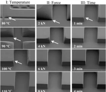
The empirical determination of optimal embossing parameters can be an extraordinarily expensive proposition unless reason-able initial boundary conditions are applied. As indicated in the sample Zeonor 750R (Tg = 72.2 uC) parameter matrix
(Fig. 5), at Temb = Tg + 8 uC, we observed partial motif
transfer and only at 110 uC, 38 uC above Tg, did we achieve
complete edge filling without a propagating rim and without stiction artefacts.
Similarly, having identified an optimal Temb we confirmed
an appropriate Fembfor a 100 mm stamp holding one device.
As one might expect due to the superposibility principle, lower forces (2 kN, 4 kN) were insufficient to achieve complete edge filling. At 6 and 8 kN, we observed faithful motif replication. Moderately higher embossing forces improved the replication uniformity without incurring rebound or elastic response defects.
Since our embossing cycle routinely involves a heating ramp of 10 uC per minute and a much slower cooling ramp of
1–2 uC per minute, the actual residence time at the embossing plateau was unsurprisingly non-critical. Nevertheless, one minute plateaux were determined to be insufficient for Zeonor 750R as indicated by slightly rounded corners.
Prioritizing Temb, Femb, and tembis often determined by the
device to be fabricated and the required yield. Cycle times can be reduced by increasing the embossing force, but in the absence of an appropriate annealling step, residual stresses can be trapped in the material. Higher embossing temperatures reduce the viscosity of the polymer melt and allow for lower forces and shorter embossing plateaux, however the con-sequences include heat damage, thermal expansion and longer cycles due to increased temperature ramp time. We favoured gentle embossing parameters, maintaining the substrate as close to thermodynamic equilibrium as possible at all times.
Correlation with DMTA
Thermoplastic lab-on-chip devices require high-modulus materials at ambient conditions and low-modulus materials under embossing conditions. The storage (E9) and loss (E0) moduli, as shown in Fig. 6, provide data for the rational choice
Fig. 5 Effect of embossing temperature (I), embossing force (II) and embossing time (III) on Zeonor 750 R, a poly(cyclic olefin). For the temperature series (I), the static embossing parameters were force (Femb) = 7 kN, embossing time (temb) = 5 min and the de-embossing
temperature (Td) = 60 uC. For the embossing force series, the static
parameters were: embossing temperature (Temb) = 110 uC, temb= 5 min
and Td= 60 uC. For the embossing time series, the static parameters
were: Temb= 110 uC, Femb= 8 kN, and Td= 60 uC (channel width
50 mm).
Fig. 6 Storage (E9) and loss (E0) moduli as well as the loss tangent (tan d) for the commercial poly(cyclic olefins) Zeonor 750 R and Zeonor 1060 R. Data measured at 1 Hz, strain = 0.2%, heating rate = 2 uC min21on a Rheometric Scientific DMTA V.
of Temb. E9 is a measure of the stored energy and E0 refers to
the energy dissipated by the polymer when a dynamic strain is applied. The loss tangent (tan d) is the ratio E0(v)/E9(v) and describes the damping of the system. Maxima in this value indicate a change in molecular, polymer or segmental motion such as the glass or melting transitions. The single peak indicates a single relaxation process in these temperature ranges. We typically emboss Zeonor 750R and Zeonor 1060R at 110 uC and 140 uC respectively. As indicated in Fig. 6, these temperatures correspond to the cusp of the viscous regime where the viscous component of the polymer behaviour is dominant and the forces measured correspond to masses below the detection limit of the instrument. Therefore DMTA provides a means to target optimal embossing temperatures in polymer films that behave as bulk materials.
Fidelity of replication
Replication fidelity can be extraordinarily good with optimal embossing parameters. As indicated by the contact profilo-metry data in Table 2, stamp features on the order of 20 mm high are transferred almost perfectly into the thermoplastic polymer. The resulting slightly deeper trench dimensions are due to the compression and rebound of the polymer during the embossing cycle. Optical profilometry, as shown in Fig. 7, is also a useful method for the rapid and non-destructive characterization of microfluidic motifs including cruciform structures, splitters and serpentine races.
Conclusions
Hot embossing of microfluidic devices provides enormous parameter space for optimization. The micro- and nano-displacement of thermoplastic polymers above their Tgoffers a
rich mechanism for the study of micro- and nano-rheology and underscores the need for further examination of related interfacial phenomena. While brute-force optimization matrices and rule-of-thumb equations may yield acceptable embossing parameters, DMTA data provide clear indications for optimal Temb. Correlation among the embossing
para-meters remains to be fully determined, though with our EVG520HE, the overall cycle-time (y30 minutes) is somewhat limiting in this regard. However, with a rationally selected
embossing temperature and minimal variation in temb, the
optimal embossing force is the only remaining significant process parameter to be determined with our tool. Our primary criterion was the high fidelity replication of micro-fluidic motifs while minimizing the embossing temperature and force. High throughput is assured by the massive paralleliza-tion that is possible with this lithographic method. Process optimization and interfacial science notwithstanding, HEL is a powerful technique for the high fidelity replication of micro-and nano-motifs from micro- micro-and nano-fabricated stamps.
Acknowledgements
The authors are grateful for financial support for the IMI-Micralyne partnership from IRAP-PARI and for technical support from Arnaud Ott, Yves Simard and Pierre Sammut. SCJ thanks the NRC for an IRF award. NSC is grateful for fruitful discussions with Dr G. Cross (Trinity College Dublin).
References
1 B. D. Gates, Q. Xu, M. Stewart, D. Ryan, C. G. Willson and G. M. Whitesides, Chem. Rev., 2005, 105, 1171–1196.
2 www.micralyne.com, www.nilfab.com, www.nilcom.org.
3 M. L. Hupert, M. A. Witek, Y. Wang, M. W. Mitchell, Y. Liu, Y. Bejat, D. E. Nikitopoulos, J. Goettert, M. C. Murphy and S. A. Soper, Proc. SPIE–Int. Soc. Opt. Eng., 2003, 4982, 52–64. 4 P. Bley, ‘Micromachined Devices and Components V’, Proc. SPIE
– Int. Soc. Opt. Eng., Santa Clara, CA, USA, 1999.
5 M. W. Mitchell, X. Liu, Y. Bejat, D. E. Nikitopoulos, S. A. Soper and M. C. Murphy, ‘Microfluidics, BioMEMS, and Medical Microsystems’, Proc. SPIE – Int. Soc. Opt. Eng., San Jose, CA, USA, 2003.
6 M. Esch, S. Kapur, G. Irizarry and V. Genova, Lab Chip, 2003, 3, 121–127.
7 S. Y. Chou, P. R. Krauss and P. J. Renstrom, Appl. Phys. Lett., 1995, 67, 3114.
8 N. S. Cameron, A. Ott, H. Roberge and T. Veres, Soft Matter, 2006, DOI: 10.1039/b600936k.
9 H.-C. Scheer and H. Schultz, Microelectron. Eng., 2001, 56, 311–332.
10 J. M. G. Cowie, Polymers: Chemistry and Physics of Modern
Materials, Chapman & Hall, New York, 1994.
11 A. Eisenberg, in Physical Properties of Polymers, 1984, pp. 54–95. 12 D. J. Plazek and K. L. Ngai, in Physical Properties of Polymers
Handbook, ed. J. E. Mark, AIP Press, New York, 1996, vol. 1,
pp. 139–159.
13 G. L. W. Cross, B. S. O’Connell and J. B. Pethica, Appl. Phys.
Lett., 2005, 86, 081902.
14 G. L. W. Cross, R. M. Langford, B. S. O’Connell and J. B. Pethica,
Mater. Res. Soc. Symp. Proc., 2005, 841, R1.6.1–12.
15 G. L. W. Cross, B. S. O’Connell, J. B. Pethica, H. Schultz and H. C. Scheer, Microelectron. Eng., 2005, 78–79, 618–624. 16 L. A. Utracki, Clay-containing polymeric nanocomposites, Rapra
Technology Limited, Shrewsbury, 2004.
17 N. S. Cameron, H. Roberge, T. Veres, S. C. Jakeway and H. J. Crabtree, Polymer Processing Society Americas Regional
Meeting, Quebec, Canada, 2005.
18 J. A. Forrest and K. Dalnoki-Veress, Adv. Colloid Interface Sci., 2001, 94, 167–196.
19 O. Prucker, S. Christian, H. Bock, J. Ru¨he, C. W. Frank and W. Knoll, Macromol. Chem. Phys., 1998, 199, 1435–1444. Table 2 Contact profilometry of silicon stamp and resulting device (RMS roughness = 30 A˚ )
Channel position Beginning Middle End
Silicon stamp (feature height/mm) 22.030 ¡ 0.002 21.040 ¡ 0.0004 22.560 ¡ 0.001 Polymer chip (feature depth/mm) 22.090 ¡ 0.014 21.090 ¡ 0.038 22.680 ¡ 0.007
Fig. 7 Optical profilometry of embossed devices (Zeonor 1060R): cruciform structure (left), splitter (middle) and serpentine race (right), structure depth = 20 mm , channel width 50 mm.
20 R. A. L. Jones, Curr. Opin. Colloid Interface Sci., 1999, 4, 153–158.
21 R. S. Tate, D. S. Fryer, S. Pasqualini, M. F. Montague, J. J. de Pablo and P. F. Nealey, J. Chem. Phys., 2001, 115, 9982–9990. 22 D. S. Fryer, R. D. Peters, E. J. Kim, J. E. Tomaszewski, J. J. de
Pablo, P. F. Nealey, C. C. White and W.-l. Wu, Macromolecules, 2001, 34, 5627–5634.
23 J. H. van Zanten, W. E. Wallace and W.-l. Wu, Phys. Rev. E, 1996, 53, R2053–R2055.
24 S. Sills, R. M. Overney, W. Chau, V. Y. Lee, R. Miller and J. Fromer, J. Chem. Phys., 2004, 120, 5334–5338.
25 G. L. W. Cross, M. Despont, U. T. Du¨rig, K. E. Goodson, W. P. King, H. Rothuizen, G. K. Binnig and P. Vettiger, personal communication.
26 H. Schift, S. Saxer, S.-G. Park, C. Padeste, U. Pieles and J. Gobrecht, Nanotechnology, 2005, 16, S171–S175.
27 W. Wu, B. Cui, X.-y. Sun, W. Zhang, L. Zhuang, L. Kong and S. Y. Chou, J. Vac. Sci. Technol., B, 1998, 16, 3825–3829.