HAL Id: hal-03118547
https://hal.archives-ouvertes.fr/hal-03118547
Submitted on 26 Apr 2021
HAL is a multi-disciplinary open access archive for the deposit and dissemination of sci-entific research documents, whether they are pub-lished or not. The documents may come from teaching and research institutions in France or abroad, or from public or private research centers.
L’archive ouverte pluridisciplinaire HAL, est destinée au dépôt et à la diffusion de documents scientifiques de niveau recherche, publiés ou non, émanant des établissements d’enseignement et de recherche français ou étrangers, des laboratoires publics ou privés.
Integration platform for optical switching of magnetic
elements
Elzbieta Sobolewska, Johan Pelloux-Prayer, Hanna Becker, Guanqiao Li, Carl
Davies, Clemens Krückel, Luis Avilés Félix, Aurélien Olivier, Ricardo C.
Sousa, Ioan-Lucian Prejbeanu, et al.
To cite this version:
Elzbieta Sobolewska, Johan Pelloux-Prayer, Hanna Becker, Guanqiao Li, Carl Davies, et al.. Inte-gration platform for optical switching of magnetic elements. SPIE Nanoscience + Engineering, Aug 2020, Online Only, United States. pp.78, �10.1117/12.2567662�. �hal-03118547�
Integration platform for optical switching of magnetic elements
E. K. Sobolewskaa, J. Pelloux-Prayera, H. Beckera, G. Lib, C. S. Daviesb,C. J. Krückelc, L. Avilés-Félixd, A. Olivierd, R. C. Sousad, I. L. Prejbeanud, A. I. Kirilyukb,
D. Van Thourhoutc, T. Rasing b, F. Moradia and M. J. R. Hecka*
a Department of Engineering, Aarhus University, Finlandsgade 22, Aarhus, Denmark, 8200; b Institute for Molecules and Materials, Radboud University, AJ Nijmegen, The Netherlands,
6525
c Photonics Research Group, Department of Information Technology, Ghent University—
IMEC Ghent, Belgium, 9052
d Spintec, Université Grenoble Alpes, CNRS, CEA, Grenoble INP, IRIG-SPINTEC,
Grenoble, France, 38000 ABSTRACT
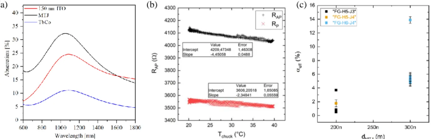
We present a detailed investigation of a novel platform for integration of spintronic memory elements and a photonic network, for future ultrafast and energy-efficient memory. We designed and fabricated magnetic tunnel junction (MTJ) structures based on (Tb/Co)x5 multilayer stack which magnetization is optically switchable. Single-pulse measurements allowed us to estimate the value of the stray field present in the parallel configuration, which prevents the structure from switching. Based on the obtained ellipsometry results of (Tb/Co)x5, we performed numerical calculations based on the Finite Difference Time Domain (FDTD) method to obtain absorption by MTJ structure. We implemented experimental results into the thermal model to estimate effective absorption in the pillar, which shows up to 14% absorption in 300-nm-wide MTJ. Moreover, we designed and realized an optical network with focusing structures to efficiently couple the light into the MTJs. Obtained results show the path to combine photonic and spintronic elements into an efficient, fast and scalable integrated system.
Keywords: integrated photonics, photonic, spintronic, terbium, cobalt, all-optical switching,
plasmonic, magnetic memory
1. INTRODUCTION
Development of more efficient data storage elements with higher bandwidth in integrated circuits has become an interdisciplinary effort for the past decade. The all-optical magnetisation reversal of magnetic layers in the magnetic tunnel junction (MTJ) elements with picosecond optical pulses [1] is of particular interest as it shows the potential for energy-efficient and fast magnetoresistive random access memory (MRAM) [2].This approach requires memory elements that are optically and electronically accessible, for optical writing and electronic read-out. In addition, it needs a photonic switching network that couples to the MTJ elements, and can route and deliver the pulses at a low optical loss with low energy consumption.
2. MATERIALS AND METHODS
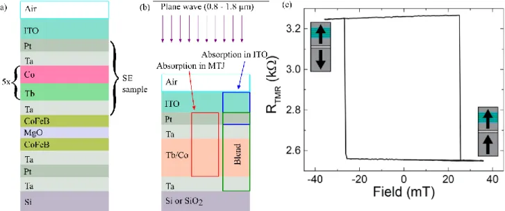
After the optical observation of all optical single pulse switching of the Tb/Co half electrode [1][4] we fabricated the MTJ electrode [5]. The device consists of the MTJ stack shown in Figure 1 - (a) and is topped with a 150 nm ITO layer. The Tb/Co bilayer was repeated 5 times in the MTJ stack and is magnetically coupled to the top CoFeB layer. Deposition process of all layers was optimized to achieve the best performance of the magnetic tunnel junction elements [1] [6]. Performance of the device was established by measuring the resistance dispersion between the low and high resistance states of MTJs. Typical high resistance state (RAP) corresponded to the storage layer’s magnetization in anti-parallel state to the top “sensing layer” where the low resistance state (RP) was obtained for the parallel state (Figure 1c) [1] [7].
2.1 Structure of the multilayers stack
Knowledge about the optical properties of the materials in the multi-layers stack is crucial for estimation of the switching power and absorbed energy. Most of the materials used in the MTJ pillar is well known. However, there were not many references for the most essential for AOS mechanism materials (Tb, Co). For that purpose, we characterized the samples with the spectroscopic ellipsometry in as-deposited state and after each of the annealing steps. Fullsheet film samples were annealed in the vacuum for 10mins at 250C and subsequently again for 10min at 300C.
Figure 1 Schematic representation of (a) The multilayer structure of the full device;(b) Simplify structure of the stack for ellipsometry measurements and FDTD calculations of reflection, transmission and absorption. (c) The magnetic field hysteresis of MTJ device. The resistance of the TMR in a function of the applied magnetic field.
Ellipsometry measurement was done with a Sentech SE 850 PV spectroscopic ellipsometer (SE) in a range from 0.7µm to 1.8µm and at incidence angles of 60, 65 and 70. From SE measurements, we obtained a set of the Δ and ψ that are related to the ratio of amplitudes for both polarization of the reflected light and their phase shift, respectively and described by the standard equation [8]:
=𝑅𝑝
𝑅𝑠 = tan(𝜓)𝑒
𝑖Δ (1)
The Kramers-Kronig regression model for the ellipsometry parameters Δ and ψ determined the optical constants of measured thin films [9]. To analyse obtained data we constructed 2 optical models consisting of Si substrate and other layers present in the sample.
First model assumed all repeated layers of Tb and Co as a one layer with sum of their thicknesses. Second approach used effective medium approximation to calculate complex refractive index of all the thin films in the stack as one layer. For the estimation of the dielectric function, the analysis was based on a parametric model consisting of Drude-Lorentz oscillator model for Tb and Tb/Co thin films and a series of layers with known optical parameters (Pt, Ta [11], Cu [12], Si [13]). Thicknesses of all layers were investigated during the optimization process, and for SE were used as input parameters and kept fixed through the fitting process. The top layer (Pt) was assumed as a perfect thin film due to neglectable roughness of the surface (RMS<0.5 nm). We used those models for samples consisting different Tb:Co ratio (1.1:1.5; 1.4:1.5 and 1.3:1.5), and further adjust them to the structure changes due to annealing process.
For estimation of the absorbed power by the MTJ multilayers stack, we used commercially available Finite Difference Time Domain (FDTD) simulation tool from Lumerical Solution Inc. [14]. We established 2D numerical model with a maximum mesh (“Yee-cell”) size of 1 nm in both lateral and vertical sides. To mimic structure of the sample, the simulation cell contained a multilayers stack of Air/ITO(150 nm)/Pt(2 nm)/Ta(2 nm)/[Tb/Co](13 nm)/CoFeB(2 nm)/MgO(3 nm)/Si(5000 nm). Due to computation requirements and simulation’s time, the second layer of Ta (0.2 nm) and all metallic layers below MgO were not included in the model (Figure 1 (a)). The small size of the pillar (max 300 nm) comparing to the spot size of the light (2400 nm) allowed implementing the plane wave as a source of the light in the 600 – 1600 nm wavelengths range with polarization parallel to x-axes. The size of the simulation region was set to the size of the largest MTJ (300 nm). To suppress unwanted reflections, a perfect matching layer (PML) and Bloch boundary conditions were set in x and y direction, respectively. To accurately reproduce the experimental conditions, we applied a complex refractive index for ITO and Tb/Co based on our spectroscopic ellipsometry measurements. We interpolated the optical parameters of Pt, Ta, CoFeB [19], MgO [20] and Si to fit into our FDTD model.
We compared our reflection and transmission results with analytical calculations based on the analytical transfer matrix method [9][15]. This comparison allowed us to confirm the correctness of the model and calculate absorption profile of Tb/Co, ITO and MTJ layers using the relation [16][26]:
𝑃𝑎𝑏𝑠= −0.5𝜔|𝐸|2𝐼𝑚(𝜀) (2)
2.2 Thermal model
All-optical switching effects are mainly characterised in term of optical fluence required to trigger it in the fullsheet film sample. These values cannot simply be applied to patterned structure below diffraction limit [17][18], due to the modification of the absorption of the laser pulse by the size and shape of the pillar. To obtain an AOS threshold values for a patterned structure, the effective absorption of the laser pulse must be evaluated [18].
For that purpose, we applied a lumped elements model as a thermal equivalent model for the MTJ, where we considered that our MTJ is a reservoir with a mean thermal resistance and a mean heat capacitance. We computed these values for the full MTJ structure with literature values of thermal conductivity for each of the layers [Table 1 ref.]. The thermal model was built on the basic principle of heat conduction in a material slab [25][26]:
Q t = κA
( Thot− Tcold)
𝑑 (3) Where Q is the heat transferred in the time t, κ is the thermal conductivity of the slab, A is the surface area normal to the heat flux, Thot and Tcold are the temperature on the two sides of the slab, and d is the thickness of the slab. The thermal resistance (Rth) of each layer was taken as: d/κ, thus the equation was:
Q At=
( Thot− Tcold)
𝑅𝑡ℎ (4) This approach assumed measuring the increase of the temperature in the MTJ due to laser heating at equilibrium, meaning that the heat flux is constant: heatin = heatout. This allowed us to ignore the thermal capacitance of the materials and to consider each part of the junction as thermal resistors connected in series [25]. In such a circuit under the laser irradiation (qlaser), the ITO is a thermal insulator (RthITO), whereas the bottom contact is thermally conductive (Rthbot).
Here, we considered that most of the measured temperature difference during the drop of the MTJ’s resistance is due to the increase of the temperature inside the MTJ’s structure and not in the ITO top contact. For simplicity, the contact and substrate are taken as cylinders of the same diameter as the MTJ. The heat capacitance was computed from the heat capacity at constant pressure and the density of the materials. Thus, we could sum the values of Rth of the different layers to get the total Rth of the MTJ excluding the ITO layer. Separating the resistances of top and bottom contact allowed us to exclude the Seeback effect during the measurements.
Figure 2 Equivalent circuit of thermal model of heat flow in an MTJ during laser irradiation (qlaser).
In this model, we considered that the thermal resistance of the top contact act as a resistor in parallel with the MTJ resistor, and the equivalent thermal resistance from the circuit can be expressed by:
𝑅𝑡ℎ𝑒𝑞= (𝑅𝑡ℎ𝑀𝑇𝐽+𝑅𝑡ℎ𝑏𝑜𝑡)𝑅𝑡ℎ𝑡𝑜𝑝
(𝑅𝑡ℎ𝑀𝑇𝐽+𝑅𝑡ℎ𝑏𝑜𝑡)+𝑅𝑡ℎ𝑡𝑜𝑝 (5)
Which leads to the equation for the heat flow (q_heat) through the MTJ in the equilibrium: 𝑞ℎ𝑒𝑎𝑡 = Q AMTJ∙t= ( TMTJ−T0) 𝑅𝑡ℎ𝑒𝑞 = Tmeas 𝑅𝑡ℎ𝑒𝑞 (6) Where both T0 (a room temperature), and Tmeas (TMTJ-T0 ) came from performed experiment.
It was possible to estimate the coupling efficiency αeff of the MTJs, by comparing the qheat value to the measured out-coupled laser power:
αeff =𝑞ℎ𝑒𝑎𝑡∙𝐴𝑀𝑇𝐽
𝑃𝑙𝑎𝑠𝑒𝑟 (7)
Table 1 Thermal resistances and heat capacitances for layers used in the equivalent model.
2.3 Single pulse switching measurement
The coercive field of the Tb/Co bilayer lies typically above 100 mT which is outside of our experimental capacities. However, the bottom CoFeB layer has a typical coercive field below 30 mT (see figure 1(b)). This allows us to measure the tunneling magneto resistance as a function of the applied magnetic field where the magnetization of the bottom CoFeB layer is changed with respect to the magnetization of the top CoFeB layer which is coupled to Tb/Co. In the case where the magnetic top and bottom layers are parallel with respect to each other we observe a relative low resistance while in the case of a antiparallel configuration we observe a relative high resistance.
We performed two experiments were we excited the MTJ device with a laser pulse with a pulse duration of 2 ps and a central wavelength of 800 nm at a fluence of 20 mJ cm-2. After each pulse we measured the voltage of the device as a function of the applied magnetic field using a Keithley 2700 multimeter under a DC current of 5 μA was provided by a Keithley 2400 sourcemeter.
Rth (10-9 m2 K/W) Cth (10-15 J/K m2)
MTJ 1.50 2.55
Pt bottom contact 1.43 0.53
ITO top contact 14.7 28.2
2.4 Grating couplers
Successful photonic-spintronic integration requires layer couplers, which are able to vertically couple optical signals up/down to the spintronic elements, depending on the integration strategy. The silicon photonics platform offers a high-refractive index contrast and thus enables compact device design and high photonic integration densities. Diffractive grating couplers are the standard method for coupling optical signals into the silicon photonic chip [21] and have the potential for highly-efficient coupling [22].
The compact out-of-plane FGC were designed with footprints of around 5x5μm2 for the 1D components and around 10x10μm2 for the 2D FGCs. Device areas in this range allow for both: optical-bandwidths exceeding the 100nm simulation window and diffraction limited focusing to micron-/submicron sized focal spot sizes [23]. The design relies on the phase matching condition to ensure constructive interference in the focal spot. The resulting curved and chirped 1/2D gratings were optimized based on a coupled simulation routine using MATLAB and a full 3D finite-difference time-domain (FDTD) simulator, using a commercial-grade FDTD electromagnetic simulation software [14].
3. RESULTS AND DISCUSSION 3.1 Optical properties
For spectroscopic ellipsometry, we used multilayer structure marked in Figure 1 (a) and deposited on a silicon substrate. Due to a strong dependence of transparent conductive oxide’s (TCO) optical properties on deposition conditions, we used samples without the ITO electrode, which was measured separately. Additionally, the first capping layer of Ta was substituted for Cu layer as presented on a first version of AOS-MTJ [1]. The complete investigated multilayers stack was built with Si/Ta(30Å)/[Co(15)/Tb(tTb)]x5/Cu(20Å)/Pt(30Å), where the thickness of the Tb (tTb) varied from 1.1 to 1.5. The samples were annealed in the vacuum for 10mins at 250C and subsequently again for 10min at 300C. We characterized the samples with the spectroscopic ellipsometry in as-deposited state and after each of the annealing steps.
To estimate the complex refractive index (ñ) of materials based on the ellipsometry measurement required buildingan analytical model that consists of the stack of materials with particular thicknesses. For that matter, we compared results from 3 different analytical models: “multilayers”, “single-layer” and “blend”. The thicknesses of all layers were fixed during the entire analysis. For platinum, copper and tantalum, we used known optical constants and left only the Tb/Co as a fitting parameter. We additionally used the optical constant of cobalt [27] in the “multilayer model” that replicated the original structure of the stack with 10 alternately repeated layers of Tb and Co. This model was not further investigated since it could not fit the data with the quality of the fit (the mean square error – MSE[9]) below 8. Such a high value of the MSE might suggest insufficient data for Co in the NIR region.
Introducing the Tb/Co as a “single-layer” with a thickness of their sum showed a significantly higher quality of the fitting procedure (MSE < 1). Results for the best fit are presented in Figure 3. Samples with all investigated Tb’s thicknesses showed very high values of the Tb/Co’s complex refractive
index (Fig.1a), which agreed with a primary assumption based on results presented by Palik et al. of Tb [28] and Co [29] separately. Annealing of the samples at 250°C changed the results insignificantly. This behaviour is characteristic of the multi-layers pile with “crystalline-like structure” [30]. The repeatable layers with the nanometre scale thicknesses create an arrangement similar to the lattice of the crystal. Such a structure is more resistant to the temperature as well as show higher RI than in case of the amorphous form with same materials composition [31]. Substantial improvement of the quality of the fitting could also suggest that instead of the clear interface between Tb and Co, we might have a structure closer to the TbCo alloy.
Additional annealing at 300°C followed by the ellipsometry measurement with the same analytical model as before showed significant changes of Tb/Co layer’s RI. Observed real part’s Re[ñ] modifications happened in two wavelengths region. For wavelengths below ~1µm, the refractive index increased by ~40% compared to the as-deposited sample, where for the region above 1.3µm decreased ~30%. These changes in the structure’s morphology were results of the annealing in the high temperature. On the other hand, the extinction coefficient showed a significant decrease in both regions around 1.2µm. Reduction of ~89% of Im[ñ] at 1.55 relates directly to decrease of the absorbed optical power, which could explain observed lack of AOS in MTJs after annealing at 300°C [1]. Even though the quality of the fit was at the acceptable level, it was much higher than before annealing for the same model and sample (MSE ~10 [32]).
Third analytical model (based on effective medium approximation) assumed consisting only 3 materials; air, “blend layer” (all the layers between ITO and Si) and Silicon substrate (Figure 3 - c). Here, the MSE decreased to below one for the sample annealed at 250°C, and below two for the further annealing at 300°C, which suggested the high quality of the fitting process. Annealing procedure is usually performed to improve the crystallinity of the structure and their optical properties [33][34][35]. However, in most cases, the investigated materials where oxides and semiconductors, due to their crystalline properties. Here, the decrease of the refractive index due to heating supported the hypothesis of MTJ’s crystalline-like structure. During the annealing, the morphology and interfaces between layers underwent changes leading to more amorphous characteristic. Performing the annealing at high temperature with the access of air can introduce a generation of oxides with some of the metallic layers. Presence of the oxides in not-crystalline form would decrease the optical parameters of the stack [36][37]. The much lower complex refractive index of “the blend” in comparison to the previous method is understandable, due to the presence of other metals in the stack. Especially Cu, Ta and Pt show Re[ñ] with their values in the range of 1-2 for NIR range. The strong decrease of the extinction coefficient in the region above 1.4µm suggested a significant influence of Tb/Co multilayers to entire MTJ.
Figure 3 Near infrared refractive index Re[ñ], and extinction coefficient Im[ñ] of Tb1.1/Co1.5 structure based on the spectroscopic
ellipsometry results with single layer model: (a) before and after annealing at 250°C, (b) the sample followed by annealing at 300°C. (c) Complex refractive index of the layers’ “blend” (Pt/Cu/(Tb/Co)/Ta) annealed at 250°C and subsequently at 300°C.
Unneglectable optical losses in each of the layers in the stack, requires taking into account all the materials present in the pillar for estimating the absorption of the MTJ. Based on obtained results from the ellipsometry measurements, we build numerical model of the multilayers stack to estimate the optical energy that is absorbed by the elements responsible for AOS. In our model, the absorption of the MTJ included all the metallic layers between ITO and CoFeB (Figure 1 - b). Preliminary simulation’s results of ITO showed that the type of the underlying material and substrate had a crucial influence for the reflection (R), transmission (T) and absorption (A) of the material. Numerical results were compared with experimental one [6] and a showed similar trend of R, T, A curves. We observed a discrepancy of a dozen of percentage in favour of calculations, which is expected occurrence, due to perfect conditions in the simulation model as well as possible differences of optical parameters of the substrate and Pt thin film. Changing the substrate from SiO2 to Si resulted in an increase of the reflection at 1550 nm wavelength from ~11% to 31%, and decrease of the transmission from ~67% to 52%. Those changes are natural consequences of a higher difference in refractive index between substrate and ITO.
After implementing additional materials presented in the stack, we performed a series of FDTD calculations to obtain absorptions of each layer (Figure 4 (a)). In our model, the ITO layer contained ITO and Pt, and MTJ layer covered Pt, Ta and (Tb/Co) thin films. Due to additional metals in the stack, the reflection increased from 31% (ITO + Pt) to 48% at 1550 nm wavelength. Based on this model, we calculated that the MTJ layer absorbs around 17.5% of the optical power at 1550 nm, with a maximum peak of ~32% at 1050 nm. We noticed that a similar percentage of the energy is lost due to absorption in ITO (~16.9% at 1550 nm, with a peak of ~24.5% at 1088 nm). Absorption in the junction can be increased by implementing antireflection coating or fabricate an additional structure that can enhance the electromagnetic field around the pillar.
3.2 Coupling efficiency
We aim at characterizing AOS events in nanometer-scaled MTJ pillars, for which optical absorption values are key parameters in estimating the optical power required to switch the AOS-layer. Here, we describe the estimation of the optical absorption in MTJ pillars of 200nm and 300nm diameter using laser light at a wavelength of 1550nm. By measuring the thermal dependence of the MTJ’s
resistive high state and low state, we can calculate the effective absorption of the laser light by the pillar.
We calibrated the electrical characteristic of measured MTJs with an externally controlled temperature and used this calibration to estimate an increase of the heat generated by the incident laser light (ΔTlaser). We used a thermal equivalent model [38][39] of an MTJ structure to calculate the power required to generate a particular temperature’s increase (qheat). Comparing this power to the incident laser power, we retrieved an effective absorption coefficient.
At first, we calibrated the MTJ thermal response with an external thermo-electric controller (TEC) by measuring the resistance of MTJ (RMTJ) at various temperatures (Figure 4- (b)). Using linear regressions, we extracted a temperature coefficient of resistance (αAP/P) [40] with temperature’s variation for both MTJ states. The temperature difference during the experiment without controlled TEC can be calculated from the change in the resistance, described by:
𝑇1𝑀𝑇𝐽𝐴𝑃/𝑃−𝑇2𝑀𝑇𝐽𝐴𝑃/𝑃 =𝑅𝑀𝑇𝐽 𝐴𝑃/𝑃(𝑇 1)−𝑅𝑀𝑇𝐽 𝐴𝑃/𝑃(𝑇 2) 𝛼𝐴𝑃/𝑃 (8)
The laser incident on the MTJ was expected to have two thermal effects. Firstly, the absorption of the laser by the MTJ raises the temperature of the pillar. Secondly, a vertical alignment of the laser and progressively occurred absorption through the MTJ (Beer-lambert’s law) lead to the thermal gradient across the device. The thermal gradient generates a thermal voltage (Vth) in an MTJ structure, known as the Seebeck effect [41][42]. The thermally influenced resistivity of the tunnel junction and the Seebeck effect had to be considered during the measurements. To estimate and remove the latter effect, we measured the voltage across the MTJ against two symmetrical current source value (i.e. +Idc,-Idc). Since the thermal gradient from the laser generates the thermal voltage, it is independent of the current source direction. This gives us two IV relations:
𝑉𝑀𝑇𝐽(+𝐼𝑑𝑐) = +𝐼𝑑𝑐𝑅𝑀𝑇𝐽+ 𝑉𝑡ℎ
𝑉𝑀𝑇𝐽(−𝐼𝑑𝑐) = −𝐼𝑑𝑐𝑅𝑀𝑇𝐽+ 𝑉𝑡ℎ (9) Combining these two equations (9) gives the MTJ’s resistance:
𝑅𝑀𝑇𝐽=𝑉𝑀𝑇𝐽(+𝐼𝑑𝑐)−𝑉𝑀𝑇𝐽(−𝐼𝑑𝑐)
(+𝐼𝑑𝑐)−(−𝐼𝑑𝑐) (10) The MTJ’s resistance depended on the measuring current and showed a small asymmetry between polarities (Figure 5 b). The average of the two-measured voltage had a nonzero value, even without the presence of the laser, which suggested that the MTJ’s resistance asymmetry is an athermal component of Vth.
Figure 4 (a) Simulated absorption of ITO (150 nm), MTJ layer (Pt/Ta/(Tb/Co)), and in multilayers stack of (Tb/Co)x5, (b) thermal
dependence calibration of an MTJ in both high (AP) and low (P) resistive state, (c) Absorption efficiency of several MTJ, the error bars were computed from uncertainty calculation and standards deviation of the measurements.
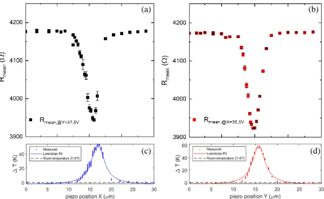
To characterize the effects of the laser light onto the MTJ, we aligned a single-mode tapered fiber (SMF) with a spot size of 2.5±0.5µm on top of the MTJ. The alignment was tracked by measuring the resistance feedback continuously from the MTJ. Proper alignment of the continuous wavelength laser (CW at 1550 nm) onto the junction leading to the drop of the resistance due to the increase of the temperature by the laser light absorption.
We performed a scan of the fiber across the MTJ using piezo controllers with 30µm travel in the XY plane to find a resistance minimum (Figure 5). Using the coefficient of resistance variation with temperature αAP/P based on Figure 4 - (b), we can calculate the temperature change of the MTJ due to the illumination of the laser (Figure 5). After alignment, we measured the resistance behaviour against the input optical power from our continuous wave (CW) laser. Which enabled us to estimate the coupling efficiency of incident optical power to absorbed optical power in the MTJ.
Figure 5 (a) and (b) The MTJ’s resistance and related to it ΔT vs fiber position in X- and Y-axis; (c) and (d) X and Y axis thermal feedback with piezocontroller alignment; full range of piezocontroller was 30 µm for each axis.
Based on the presented thermal model, we calculated the absorption efficiency for varies MTJs ( Figure 4 – (c)). We achieved the best absorption value of about 14% for a 300nm diameter MTJ and ~3.7% for a 200nm diameter MTJ. Obtained results are consistent with preliminary numerical calculation. Higher convergence for both sets of data should not be required. The numerical model presents the ideal situation excluding the influence of roughness of the layers, incidence angle and structure’s shape. Those parameters might bring additional changes in the heat distribution and change the absorption of the junction significantly.
3.3 Switching mechanism
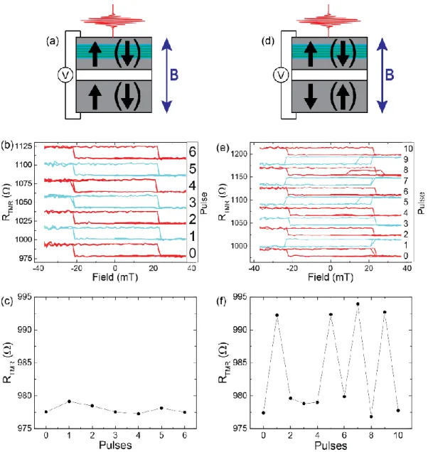
An investigation of all optical single pulse switching of the MTJ electrode was performed with the sample presented in Figure 1-(a). For the first experiment, we configured the magnetic top layer parallel with respect to the magnetic bottom layer before the arrival of each laser pulse - Figure 6-(a). After each laser pulse we measured the magnetic hysteresis as is shown in Figure 6-(b) and then extracted the resistance value of the device at 30 mT (Figure 6-(c)).
In the second experiment we applied similar procedures, however, now we configured the magnetic top and bottom layer so that it is antiparallel with respect to each other before the arrival of each laser pulse Figure 6-(d). The magnetic hystersis and resistance values after each laser pulse is shown in Figure 6-(e) and Figure 6-(f), respectively. The magnetic hysteresis at pulse 3 and 4 (Figure 6 – (c), (d)) did not show a reversal, this is due to mechanical vibrations and drifting of the sample holder resulting in occasional misses of the laser pulse onto the MTJ device target.
(a) (b)
Since the applied magnetic field is only strong enough to reverse the magnetization of the bottom layer, we can understand the switching of the top Tb/Co magnetization as observing a reversal of the magnetic hysteresis behavior. Figure 6-(b) shows that the hysteresis does not change after the laser pulse excited the MTJ device in the parallel configuration. However, Figure 6-(e) shows that the hysteresis does change after the laser pulse excites the MTJ device in the antiparallel configuration. The fact that the optical pulse has no effect on the magnetic hysteresis of the MTJ device in the parallel configuration (while in the case of the antiparallel configuration we observed a clear reversal of the magnetic hysteresis) means that the top magnetic layer must experience a stray field originating from the bottom magnetic layer. It is well known that the magnetization under an ultrashort laser pulse is suppressed at a sub-picosecond timescale [8]. During the recovery period of the magnetization, it becomes susceptible to small magnetic fields. This high sensitive during the later time can prevent the top layer from switching the magnetization from a parallel to antiparallel configuration with the bottom layer while without the bottom layer the magnetization of the top layer can switch deterministically under a single laser pulse [1], [5]. To estimate this stray field, we applied a magnetic field at various field strengths during the arrival of the laser pulse. We estimated that an average of 6.3 mT was needed to switch the MTJ device from a parallel configuration to an antiparallel configuration.
Figure 6 . (a) The magnetic layers were configures parallel pre-optical-pulse. (b) A magnetic field hysteresis was performed after each pulse and (c) the resistance at 30 mT is compared after each pulse. (d) The same experiment was performed for the anti-parallel configuration with (e) the respective magnetic field hysteresis and (f) resistance at 30 mT.
3.4 Focusing grating couplers
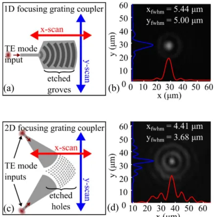
We have presented out-of-plane focusing grating couplers (FGCs) as a solution for vertical co-integration in [23]. To enable dense co-integration, the FGCs were designed for a small footprint, high-bandwidths (permitting short optical pulse handling), effective and diffraction limited focusing and were investigated both in a 1D configuration, as shown schematically in Figure 7a), and in a 2D configuration, as shown in Figure 7c). Since the binary resistivity state of the MTJs changes if the absorbed optical energy surpasses a material specific threshold value, it becomes particularly important to achieve high peak intensities within a small focal area. The 2D FGCs have the additional advantage for full-control of the emitted polarization, given the relative phase control of the two input ports [23]. Design restrictions arise from the fact that fabrication was done on the standard
220-nm-silicon-on-insulator platform available by imec [24], defining the layer stack, layer thickness and minimum design feature sizes.
We experimentally determined the focusing characteristics with a cross-scan procedure using a tapered-and-lensed fiber, evaluating the spatial coupling efficiency to the fiber. The measurements revealed the expected focusing behaviour, indicating a minimum x-/y-FWHM of 2.3μm and 2.1μm for a well-performing single-silicon-layer1 1D FGC and 1.4μm and 2.8μm x-/y-FWHM values for a well-performing 2D FGC. Given that the experimental analysis relies on the assumption of a Gaussian-like, elliptical, focused beam profile, the FGC emission was recently imaged with a custom-built high-NA microscope and an infrared camera. A recorded image of a double-layer FGC is shown in Figure 7 – (b), indicating low side-lobes and a focal spot with a low degree of ellipticity. Figure 7d) shows much more pronounced side-lobes in the case of the 2D FGC and a higher degree of ellipticity. While image magnification and resolution, as well as, poor height control of the microscope very likely increase the measured FWHM values, the images do reveal the diffraction of a considerable amount of light into the side-lobes, which is an intensity lost in the maximum peak.
The experimentally determined focusing characteristics of the designed out-of-plane FGCs reveal the unambiguous focusing behavior of the emitted beam. Measurement results for the 1D FGC show rather uniformly shaped Gaussian beam profiles and FWHM values of the focal spot of a few micrometers. Characterization of the focusing, achieved by 2D FGCs also reveal the desired focusing, but measurements imply a more distorted focal spot and intensity diffraction into focal side-lobes. With emission efficiencies not exceeding -13dB for our single-silicon-layer gratings, further optimization of these devices is needed, which should yield higher efficiencies. The double-silicon-layer gratings show the potential for improvement with simulated 74% (-1.3 dB) directionality.
Figure 7 (a) Schematic of 1D FGC, (b) Focal spot imaging with IR-camera and microscope of double-layer 1D FGC, (c) Schematic of 2D FGC, (d) Focal spot imaging of 2D FGC.
3.5 Network and output power
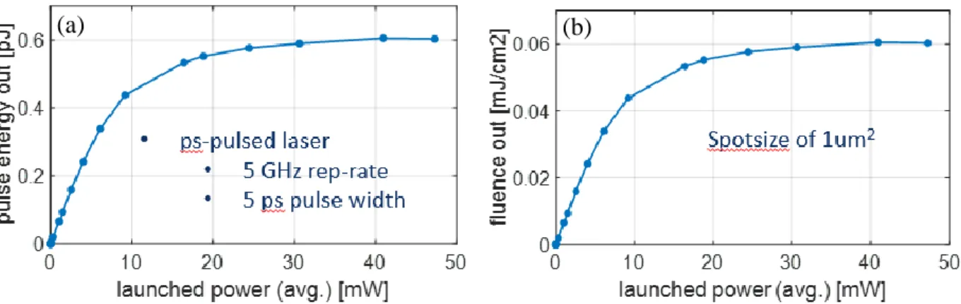
For the all-optical switching event of MTJ cells, sufficient optical pulse energy is required after the photonic distribution network. When composing the photonic network with silicon waveguides, the optical throughput may be limited due to nonlinear loss. At telecom wavelengths, the propagation loss increases with higher optical intensities originating from two-photon absorption (TPA) and consequently resulting in free-carrier absorption (FCA). The saturation of outcoupled power has been shown for CW light and silicon strip waveguides (220nmx450nm) in [43]. Here, we show the power saturation for pulsed light (5ps, 10GHz repetition rate). The experimental results are illustrated in Figure 8 (a), indicating the limitation of outcoupled optical pulse energy.
From the pulse energy, we calculated the expected optical fluence using focusing grating couplers as designed in [23]. The results are presented in Figure 8- (b). It becomes clear that the fluence is below the requirements for all-optical magnetic reversal. In order to increase this value, higher pulse energies can be achieved by reducing nonlinear absorption with active structures based on reverse biased pin-diodes [44][45] or in passive structures based on rib waveguides [43].
Figure 8 Experimental characterization of nonlinear loss is silicon strip waveguides. (a) Pulse energy after photonic chip vs. average power of optical pulse train. (b) Optical fluence after photonic chip vs. average power of optical pulse train.
4. CONCLUSION AND OUTLOOK
In this work, we showed crucial steps towards spintronic-photonic integration. The optical properties of the MTJ consisting Pt(2 nm)/Ta(2 nm)/[Tbx/Co1.5](13 nm)/ Si(5000 nm) were investigated by the ellipsometry before and after annealing. The complex refractive index of (multilayer stack of (Tb/Co)x5 was determined from a multi-sample analysis of layers with a variety of Tb’s thicknesses. Presented results showed higher than previously reported values of the refractive index and an extinction coefficient for Tb, Co or their alloys. This unique behaviour indicates the crystalline-like structure formed by alternating layers of Tb and Co in the MTJ. Those properties are steady and stable for samples annealed at a temperature below 300°C. Those parameters were implemented into theoretical FDTD model to calculate absorption in fullsheet films and into the thermal model to estimate effective absorption by the pillar (Pt(2 nm)/Ta(2 nm)/[Tbx/Co1.5](13 nm)) in the working device. Results showed high convergence of the results with max 17.5% and 14% absorption at 1550 nm for 300nm from simulations and experiments, respectively.
Single-pulse switching measurements on the MTJ electrode showed that the reversal of the magnetic hysteresis is possible only in the case of antiparallel configuration. These results suggest that the top magnetic layer becomes susceptible to small magnetic fields from the bottom layer, which in consequence prevents them from switching the magnetization from a parallel to antiparallel configuration. We estimated that the strength of a stray field that is needed to switch the MTJ device from a parallel to an antiparallel configuration is in an average of 6.3 mT. This finding shows that all-optical switching is possible regardless of the starting configuration with proper adjustment against the intrinsic stray field. Next crucial step towards proper integration is to provide an adequate amount of the laser light to the MTJs. We proposed and investigated silicon network with focusing grating couplers in terms of sufficient out-coupled energy and the spot size. We can conclude from the presented experimental data, that the silicon platform is in fact suitable for photonic integration with electronics in general for both monolithic and hybrid integration schemes. The FGCs offer a small footprint and show the potential for highly efficient coupling.
However, the footprint mismatch between the photonics to electronic technology remains large. Scaling micrometer sized and diffraction-limited photonic components to nanometer-sized electrical components remains a technological challenge. In addition, a knowledge of all the mechanisms in the AOS structure is crucial to overcome the energy losses that are limiting the performance of the integrated device. Energy improvement can be done in many ways from applying active
elements in the network, fabricating the antireflection coating on top of the MTJ up to implementing plasmonic structures for enhancing the electromagnetic field in the junction’s structures. These developments represent the first step towards the integration of spintronic-photonic system on a single chip. Feasible further optimisation of the elements opens a new path for faster memory devices with lower energy consumption.
REFERENCES
Chen, J., et al., “All-Optical Switching of Magnetic Tunnel Junctions with Single Subpicosecond Laser Pulses,” Physical Review Appllied 7, 021001, 2–7 (2017), doi: https://doi.org/10.1103/PhysRevApplied.7.021001 Kimel, A. V., Li, M., “Writing magnetic memory with ultrashort light pulses,” Nature Reviews Materials 4, 189–
200 (2019), doi: https://doi.org/10.1038/s41578-019-0086-3
Avilés-Félix, L., et al.”Single-shot all-optical switching of magnetization in Tb/Co multilayer-based electrodes”, Scientific Reports 10, 5211 (2020). https://doi.org/10.1038/s41598-020-62104-w
Ciuciulkaite, A., et al.” Design of Amorphous TbxCo100-x Alloys for All-Optical Magnetization Switching”, Applied Physics (2020)
Avilés-Félix, L. et. al., ”Integration of Tb/Co multilayers within optically switchable perpendicular magnetic tunnel junctions”, AIP Advances 9, 125328 (2019);
Olivier, A., et. al., “Indium Tin Oxide optical access for magnetic tunnel junctions in hybrid spintronic–photonic circuits”, Nanotechnology 31 (2020)
Davies, C.S., et. al., “ Pathways for Single-Shot All-Optical Switching of Magnetization in Ferrimagnets”, American Physical Society 13,024064 (2020)
Beaurepaire, E., et. al., “Ultrafast spin dynamics in ferromagnetic nickel,” Physical Review Letters 76, (22), 4250–4253 (1996)
Hilfiker, J.M. et. al.,” Survey of methods to characterize thin absorbing films with Spectroscopic Ellipsometry”, Thin Solid Films 516, 7979–7989 (2008)
Losurdo, M., Hingerl K., “”Ellipsometry at the nanoscale”, Springer Heidelberg New York Dordrecht London, 1-30 (2013)
Palik, E.D., Lynch, D.W., Hunter, W.R:,”Handbook of Optical Constants of Solids I; - An Introduction to the Data for Several Metals”, Academic Press, 341-419 (1997)
Palik, E.D., Lynch, D.W., Hunter, W.R:,”Handbook of Optical Constants of Solids I; Comments on the Optical Constants of Metals and an Introduction to the Data for Several Metals ”, Academic Press, 275-367 (1997) Palik, E.D., Edwards D. F., : ”Handbook of Optical Constants of Solids I; - - Silicon (Si)*”, Academic Press,
547-569 (1997)
Nanophotonic FDTD Simulation Software - Lumerical FDTD Solutions, (2018).
https://www.lumerical.com/products/fdtd-solutions/.
Nanophotonic FDTD Simulation Software - Lumerical FDTD Solutions, “Stack optical solver overview”, (2018), Nanophotonic FDTD Simulation Software - Lumerical FDTD Solutions, “Calculating absorbed optical power -
Higher accuracy”, available online; (2018)
Le Guyader, L., et al., “Nanoscale sub-100 picosecond all-optical magnetization switching in GdFeCo microstructures,” Nature Communications 6 (2015); doi: 10.1038/ncomms6839
Savoini, M., et al., “Highly efficient all-optical switching of magnetization in GdFeCo microstructures by interference-enhanced absorption of light,” Physical Review B 86 (2012); doi: 10.1103/PhysRevB.86.140404. Surabhi, S., et al., “Precise Determination of the Temperature Gradients in Laser-irradiated Ultrathin Magnetic
Layers for the Analysis of Thermal Spin Current”, Scientific Reports 8, 11337 (2018);
https://doi.org/10.1038/s41598-018-29702-1
Stephens, R. E., Malitson, I. H., “Index of refraction of magnesium oxide”, Journal of Research of the National Bureau of Standards 49, 249-252 (1952)
Taillaert, D. F., et al., “Grating couplers for coupling between optical fibers and nanophotonic waveguides”, Japanese Journal of Applied Physics, Part 1: Regular Papers and Short Notes and Review Papers 45 (8), 6071– 6077 (2006)
Michaels, A., Yablonovitch, E., “Inverse design of near unity efficiency perfectly vertical grating couplers”, Optics Express 26 (4), 4766–4779 (2018)
H. Becker, et al., “Out-of-plane focusing grating couplers for silicon photonics integration with optical MRAM technology,” Ieee Journal Of Selected Topics In Quantum Electronics 26, (2019).
Silicon photonic ICs for prototyping, Available Online (10 June 2020) https://www.imec-int.com/en/silicon-photonic-ICs-prototyping
Pakanen, J.,” Conduction of heat through slabs and walls”, VTT Publications 169 (2009),) available online (8 August 2020), www.vttresearch.com/sites/default/files/pdf/publications/2009/P162.pdf
Nave, R., Department of Physics and Astronomy, Georgia State Univeristy, Online tutorials from physics (2016), available online (30 July 2020), hyperphysics.phy-astr.gsu.edu/hbase/thermo/heatra.html#c1
Johnson, P. B., Christy, R. W., “Optical constants of transition metals: Ti, V, Cr, Mn, Fe, Co, Ni, and Pd”, Physical Review B 9, 5056-5070 (1974)
Palik, E. D., Ward, L., „Handbook of Optical Constants of Solids III - Optical Constants of Eight Rare Earth Elements: (Ce), (Sm), (Gd), (Tb), (Dy), (Er), (Tm), and (Yb)”, Academic Press, 287 – 340 (1997)
Palik, E. D., Ward, L., „Handbook of Optical Constants of Solids II – Cobalt (Co)”, Academic Press, 435 – 448 (1997)
Pavlov, V. et al., “Ellipsometric and magneto-optical study of nanosized ferromagnetic metal-dielectric structures [Co/TiO2]n/Si”, Thin Solid Films 619 (2016)
Farmakidis et al., “Plasmonic nanogap enhanced phase-change devices with dual electrical-optical functionality”, Science Advances 29 (2019)
Hoffmann, M. A., et. al., ”Spectroscopic ellipsometry and magneto-optical Kerr effect spectroscopy study of thermally treated Co60Fe20B20 thin films”, Journal of Physics: Condensed Matter 32 (2020),
Liu, Y., et. al., “Effects of annealing temperature, thickness and substrates on optical properties of m-plane ZnO films studied by photoluminescence and temperature dependent ellipsometry”, Journal of Alloys and Compounds [In Press] (2020)
Alfonso, J.E., el. al., “Annealing Effect on the Structural and Optical Properties of Sputter-Grown Bismuth Titanium Oxide Thin Films”, Materials 7, 3427-3434 (2014)
Mahbubur Rahman, M., el. al., ” Investigation of the post-annealing electromagnetic response of Cu–Co oxide coatings via optical measurement and computational modelling”, RSC Advances 27 (2017)
Hojabri, A., Hajakbari, F., Soltanpoor, N. et al., “Annealing temperature effect on the properties of untreated and treated copper films with oxygen plasma”, Journal of Theoretical and Applied Physics 8, 132 (2014). https://doi.org/10.1007/s40094-014-0132-x
Manouchehri, I., et al., “Investigation of annealing effects on optical properties of Ti thin films deposited by RF magnetron sputtering”, Optik 127 (13), 5383-5389 (2016)
Lecture notes for Aerospace Engineering at Sapienza Università di Roma, “Chapter 3: Thermal-electrical analogy: thermal network”, available online (4 August 2020):
http://www.ingaero.uniroma1.it/attachments/2176_Cap_3%20Thermal-electrical%20analogy.pdf; Cheever, E. Department of Engineering, Swarthmore Collage, Complementary notes for course - Linear
Physical Systems Analysis; “Mathematical Models of Thermal Systems”, available online (4 August 2020): https://lpsa.swarthmore.edu/Systems/Thermal/SysThermalModel.html;
H. F. Yang et al., “Electrical measurement of absolute temperature and temperature transients in a buried nanostructure under ultrafast optical heating,” Applied Physics Letters, vol. 110, no. 23, p. 232403, Jun. 2017, doi: 10.1063/1.4985434.
M. Walter et al., “Seebeck effect in magnetic tunnel junctions,” Nature Materials, vol. 10, no. 10, pp. 742–746, Oct. 2011, doi: 10.1038/nmat3076
N. Liebing et al., “Tunneling Magnetothermopower in Magnetic Tunnel Junction Nanopillars,” Physical Review Letters, vol. 107, no. 17, Oct. 2011, doi: 10.1103/PhysRevLett.107.177201.
Krueckel, C., et al., “Impact of optical free-carrier generation on the performance of SOI phase shifters”, [in preparation].
Gajda, A., et al.” Highly efficient CW parametric conversion at 1550 nm in SOI waveguides by reverse biased p-i-n junction," Optic Express 20, 13100-13107 (2012)
Turner-Foster, A., et al.” Ultrashort free-carrier lifetime in low-loss silicon nanowaveguides," Opt. Express 18, 3582-3591 (2010)

![Figure 3 Near infrared refractive index Re[ñ], and extinction coefficient Im[ñ] of Tb 1.1 /Co 1.5 structure based on the spectroscopic ellipsometry results with single layer model: (a) before and after annealing at 250°C, (b) the sampl](https://thumb-eu.123doks.com/thumbv2/123doknet/13071126.384224/9.893.92.802.113.329/infrared-refractive-extinction-coefficient-structure-spectroscopic-ellipsometry-annealing.webp)