DEVELOPMENT OF A SELECTIVE SUBSTRATE METALLIZATION
PROCESS VIA ELECTROLESS GEL PLATING
By
Kenneth C. Arndt
B.S., Materials Science and Engineering, 1994
University of Illinois (Urbana-Champaign)
Submitted to the Department of Materials Science and Engineering
in Partial Fulfillment of the Requirements for the Degree of
MASTER OF SCIENCE
in Materials Science and Engineering
at the
Massachusetts Institute of Technology
June 1996
C 1996 Massachusetts Institute of Technology
All rights reserved
Signature of Author
Certified by
Accepted by
Department of Materials Science and Engineering
May 10, 1996
I(
Michael J. Cima
Norton Professor of Ceramics
Michael F. Rubner
TDK Professor of Materials Science and Engineering
Chair, Departmental Committee on Graduate Students
MASSACHUSETTS INSTITUTE
OF TECHNOLOGY MWAS$ACHUSMTS OF TECHNOLOGY$1UT
JAN 2
5
2007
DEVELOPMENT OF A SELECTIVE SUBSTRATE
METALLIZATION PROCESS VIA ELECTROLESS GEL PLATING
By
Kenneth C. Arndt
Submitted to the Department of Materials Science and Engineering on May 10, 1996
in partial fulfillment of the requirements for the Degree of Master of Science in Materials Science and Engineering
ABSTRACT
Advanced hybrid microelectronics require high performance packaging materials and components. Alumina, the most widely used ceramic material in microelectronics, is being replaced by new high performance materials such as aluminum nitride (AlN) and beryllia (BeO). AlN's thermal conductivity is an order of magnitude greater than alumina and it has a thermal expansion coefficient very close to silicon. Metallization is used to generate areas for wire and die bonding and to form corrosion barriers for underlying metals. Plating is one metallization process which immerses the component to be coated into a chemical medium. The plating baths usually operate at temperature greater than 70'C and a pH greater than 12. Alumina is stable in this environment but AlN corrodes.
An electroless gold gel plating process was developed which selectively plates specific areas of a surface without exposing the component to a corrosive environment. The developed process exhibits several advantages: selective area metallization, variable metal thickness on the same component, rework of defectively plated parts, reduction of waste produced during operation, optimal usage of gold, higher plating rates, and elimination of variation in the chemical composition during operation. An electroless plating gel was formulated using a modified commercial bath and a polymeric thickening agent. The relationship between gel processing and the resulting chemical and physical properties are discussed. The gel was transferred to the substrate in a defined pattern by a screen printer and then deposited in a chemical reactor. Several chemical reactors were fabricated to reduce the time required to obtain the operating temperature and decrease the drying rate during plating. The final reactor prototype increased the heating rate over five fold and decreased the drying rate by a factor of 4.
Metallic impurity contamination was discovered in residual gel samples after plating. This caused non-uniform coatings and decreased the plating rate. A chelating agent was added to the electroless gel which complexed with the metal ions preventing them from interfering in the plating reactions. Scanning electron microscopy (SEM) showed the resulting gold plate was dense and uniform.. Gold conversion efficiencies, the amount of gold plated from the gel onto the substrate surface, were determined by DCP. Conversion efficiencies were typically greater than 90% with reproducible values greater than 95%.
Thesis Supervisor: Michael Cima
TABLE OF CONTENTS
Section
Pa2e #
TITLE PAGE 1 ABSTRACT 2 TABLE OF CONTENTS 4 LIST OF FIGURES 8 LIST OF TABLES 12 ACKNOWLEDGMENTS 14 Chapter 1 INTRODUCTION 16Chapter 2 BACKGROUND LITERATURE REVIEW 20
2.1 REVIEW OF HYBRID MICROELECTRONICS 20
2.1.1 Substrate Technology 20
2.1.2 Thick Film Technology 21
2.1.3 Thin Film Technology 21
2.1.4 Co-fired Ceramic Technology 22
2.1.5 Assembly 22
2.1.6 Packaging 22
2.1.7 Advantages of Hybrid Microelectronics and Their 22 Applications
2.2 PLATING AND METALLIZATION IN MICROELECTRONICS 23
2.3 ELECTROLESS GOLD PLATING 25
2.4 SUBSTRATE MATERIALS 28
2.4.1 Substrate Cleaning 31
2.5 SELECTIVE PLATING 31
2.5.1 Selective immersion 33
2.5.3 Jet Plating 33
2.5.4 Photoselective Deposition 33
2.5.5 Electroless Gel Plating 33
2.6 SCREEN PRINTING 34
2.6.1 Effects of Rheology on Paste and Print Properties 34
2.6.2 Effects of Screen Printing Parameters on the Final Print 34 Quality
2.7 REVIEW OF DRYING 38
2.8 DRYING OF MATERIALS 38
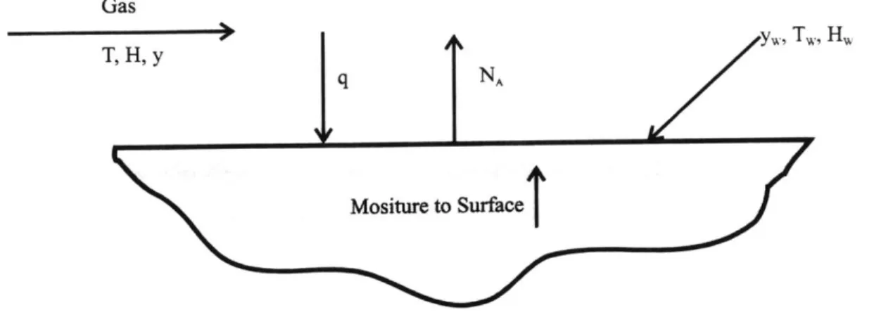
2.8.1 Unsteady-State Heat Transfer between Materials 39
2.8.2 Mass Transfer and Diffusion 41
2.8.2.1 Unsteady-State Mass Transfer and Diffusion 41 2.8.2.2 Important Mass Transfer Coefficients for Various 42
Geometries
Chapter 3 BASIC PROCESS FOR ELECTROLESS GEL PLATING 46
3.1 EXPERIMENTAL PROCEDURE 46 3.2 RESULTS 48 3.2.1 Gel Formation 48 3.2.2 Screen Printing 49 3.2.3 Deposition 50 3.3 DISCUSSION 51 3.3.1 Gel Formulation 51
3.3.2 Transfer of Gel to Substrate Surface 52
3.3.3 Deposition 53
3.4 SUMMARY 55
Chapter 4 DESIGN, FABRICATION, AND CHARACTERIZATION OF A 58
CHEMICAL REACTOR USED FOR ELECTROLESS GEL PLATING
4.1 INTRODUCTION 58
4.2 GENERAL DESIGN APPROACH 59
4.3 EXPERIMENTAL PROCEDURE 62
4.4 HEAT TRANSFER IN THE FINAL PROTOTYPE 63
4.4.1 Theoretical Results 63
4.4.2 Experimental Results 69
4.5 DRYING AND MASS TRANSFER IN FINAL REACTOR 72
PROTOTYPE
4.6 DISCUSSION OF PROPERTIES FOR REACTOR PROTOTYPES 73
4.6.1 Heat Transfer 73
4.6.2 Mass Transfer 78
5.1 INTRODUCTION 82
5.2 RESULTS AND DISCUSSION OF ELECTROLESS GEL PLATING 83
5.2.1 Formulation of Electroless Gold Gel 83 5.2.2 Screen Printing of the Electroless Gold Gel 87
5.2.3 Deposition of Gold Plate 91
5.2.4 Characterization of Electroless Gel Plated Substrates 93
5.2.5 Nickel Poisoning 94
5.2.5.1 Introduction 94
5.2.5.2 Experimental Procedure 96
5.2.5.3 Results and Discussion 97
5.2.5.4 Solutions to Nickel Poisoning 102
5.2.6 Gold Conversion Efficiency 106
5.2.7 Advanced Techniques 108
5.3 SUMMARY 111
Chapter 6 CONCLUSION AND FUTURE WORK 114
6.1 CONCLUSIONS 114
6.2 FUTURE WORK 115
ELECTROLESS GEL PLATING 82
LIST OF FIGURES
Fiture
Pa2e #
CHAPTER 2
Figure 2.1 Corrosion rate as a function of pH. " 30
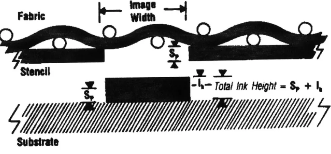
Figure 2.2 Diagram of screen printing process.' 35
136
Figure 2.3 Schematic of paste columns deposited during screen printing. 36
Figure 2.4 Heat and mass transfer in constant-rate drying.28
39
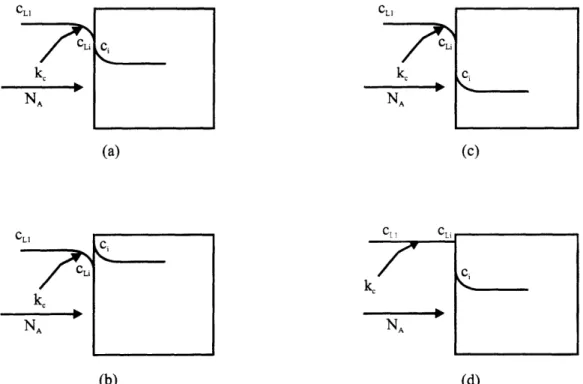
Figure 2.5 Interface conditions for mass transfer and various K. (a) K=1, (b) 42
K>1, (c) K,1, (d) K>1 and ke = oo .28
CHAPTER 3
Figure 3.1 Schematic for prototype #1. 48
Figure 3.2 Photograph of AIN substrate with a nickel/tungsten metallization 49
pattern. The 12 square pads and bus lines are nickel and the other metallized areas are tungsten.
Figure 3.3 Photograph of screen printed electroless gold gel pattern on a blank 49 alumina substrate.
Figure 3.4 Photographs of gel prints which: (a) have experienced drying, and 50
(b) have not experienced drying.
Figure 3.5 Photograph of deposited AIN substrate rinsed with deionized water 50
after
1
hour in reactor.Figure 3.6 Schematic of a gel print which fully released from an emulsion 53
screen.
Figure 3.7 Schematic of a gel print which has not fully released from the 53
screen.2
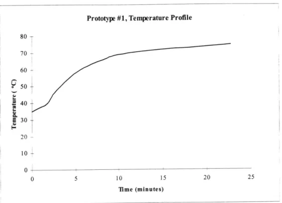
Figure 3.8 Temperature versus time heating profile for first generation 54
prototype.
CHAPTER 4
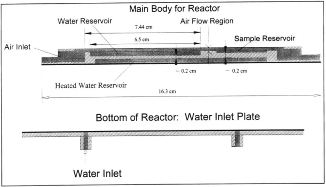
Figure 4.1 Schematic of the bottom brass cartridge for prototype #2. 61
Figure 4.2 Cross section schematics for the brass base cartridge for the final 61
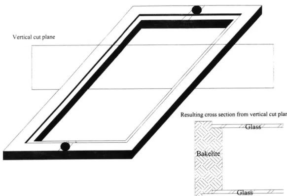
Figure 4.3 Schematic of the third generation reactor top. Fabricated from 62
Bakelite composite and Pyrex glass plates.
Figure 4.4 Figure 5.3-6 in Geankoplis used to calculate value of .5 64
Figure 4.5 Calculated temperature versus time curve for reactor prototype #3 65
from Pdease.
Figure 4.6 Blow up of Figure 4.5 temperature versus time curve. 66
Figure 4.7 Cross section of base brass cartridge for the second generation 66
prototype, providing the locations described in the legends for Figure 4.5 and Figure 4.6.
Figure 4.8 Pdease temperature contours for (a) whole reactor base, (b) blow up 67
of sample reservoir; after
1
second of operation.Figure 4.9 Pdease temperature contours for (a) whole reactor base, (b) blow up 68
of sample reservoir; after 60 seconds of operation.
Figure 4.10 Experimental temperature versus time curve for reactor prototype 69
#3. The locations b and c are described in Figure 4.7.
Figure 4.11 Blow up of Figure 4.10 showing the experimental temperature 70
versus time curve for reactor prototype #3.
Figure 4.12 Theoretical versus experimental temperature curves for prototype 71
#3.
Figure 4.13 Drying flux versus surface area for water droplets of known volume 72
in prototype #3.
Figure 4.14 Drying rate for large and small gel print pads using the drying flux 73
calculated in Figure 4.13.
Figure 4.15 Comparison of experimental temperature versus time curves. 75
Figure 4.16 Theoretical comparison of temperature versus time curves. 76
Figure 4.17 Comparison of drying flux versus surface area for prototypes #2 and 79 #3.
Figure 4.18 Time to dry printed gel pads versus various flow rates. 79
CHAPTER 5
Figure 5.1 Experimental ranking of the performance of thickening agents used 86
in this study.
Figure 5.2 Relationship between resulting gold deposit thickness, gel print 86
thickness, and gold concentration.
Figure 5.3 optical photo of the carrageenan gel after printing. (b) optical photo 87
Figure 5.4 (a) photograph of screen printed Methocel J5MS polymeric system. 88 (b) photograph of screen printed Methocel K4M polymeric system.
Figure 5.5 (a) photograph of gel print using a 200 mesh screen size. (b) 90
photograph of gel print using 80 mesh screen size. (c) optical micrograph blow-up of (a). (d) optical micrograph blow-up of (b).
Figure 5.6 Optical micrograph of an acceptable gel print utilizing the Methocel 91
K4M polymer system and a polymeric/metal mesh screen.
Figure 5.7 (a) Acceptable gel print behavior during plating. (b) Unacceptable 92
gel print behavior during plating caused by the polymer segregating out of solution.
Figure 5.8 Gelation temperature range of the hydroxypropylmethylcellulose 92
polymer in electroless gel.3
Figure 5.9 SEM micrograph of an electroless gel gold plated sample, using 93
20g/l complexing agent. (15000x's).
Figure 5.10 An optical micrograph showing the final gold plate resolution 94
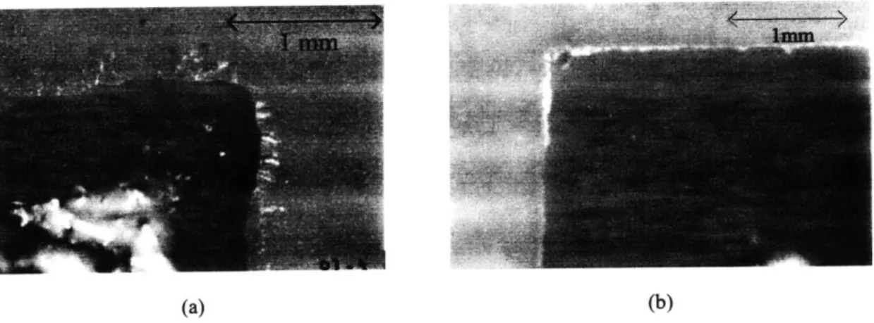
obtainable from the electroless gel process over a length of 2mm.
Figure 5.11 Optical micrograph of an electroless gel plated nickel pad. 97
Figure 5.12 (a) SEM micrograph of nickel pad plated with electroless gold gel, 98
(100x's). (b) Magnified corner of nickel pad plated with electroless gold gel, (800x's).
Figure 5.13 The structure of EDTA (a) before and (b) after metal ion capture. 102
Figure 5.14 Effects of EDTA on gold microstructure.(a) Og/L EDTA, (b) 5g/L 104
EDTA, (c) 10g/L EDTA, (d) 15g/L EDTA, (e) 20g/L EDTA. SEM
at (2000x's).
Figure 5.15 Effects of EDTA on gold microstructure.(a) Og/L EDTA, (b) 5g/L 105
EDTA, (c) 10g/L EDTA, (d) 15g/L EDTA, (e) 20g/L EDTA. SEM
at 8000x's.
Figure 5.16 SEM micrographs. (a) typical gold plate obtained from gel solutions 109
at 8g/l gold concentration and without a complexing agent, 800x's.
(b) gold plate obtained from 40g/l gold concentration without
complexing agent, 800x's. (c) micrograph in (a) at 8000x's. (d) micrograph in (b) at 8000x's.
Figure 5.17 Diagram illustrating one method to achieve selective thickness using 110
electroless gel plating.
Figure 5.18 SEM micrograph (8000x's) showing the difference in density of two 111 samples printed with a standard electroless gold gel.* (a) One print
with 8g/L electroless gold gel. (b) Three prints with 8g/L electroless gold gel. *(both samples contain 20g/l EDTA).
LIST OF TABLES
Table
Paie #
CHAPTER 2
Table 2.1 Corrosion rate of AIN substrates." 30
Table 2.2 Comparison of properties between emulsion and metal stencil 37
screens.
Table 2.3 Common problems and solutions in screen printing. 38
CHAPTER 4
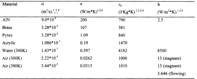
Table 4.1 Thermal properties for materials used in fabrication of the chemical 59
reactors.
Table 4.2 Values of time constants for various materials. 77
Table 4.3 Experimentally observed times for reactor prototypes to reach a 77
designated temperature.
Table 4.4 Time, drying flux, and drying rate for large gel printed pads from 78
experimental data.
CHAPTER 5
Table 5.1 Examples of the advantages and impact of electroless gel plating for 83
new packaging material.
Table 5.2 Data sheet describing the observed performance of various 84
thickening agents.
Table 5.3 Characteristics of metal mesh screens. 90
Table 5.4 DCP analysis of nickel in depleted gel residue. 101
ACKNOWLEDGEMENTS
I would like to dedicate this thesis to my family who has instilled in me the motivation and desire
to follow my dreams. I would like to thank my parents for providing all the love and support I needed throughout my education, and for taking such a strong interest in my accomplishments. I would like to thank my sisters Jenny and Sarah and my brother David who have given me their support and their compassion in the pursuit of my goals. Many times I have turned to them and they have listened, I hope that I can follow their examples and return their favors many fold.
I would like to thank my advisor, Michael Cima, for guiding me through the maze of materials science known as processing. It has been adventurous and surprising not knowing what the next experiment will bring, I hope that this excitement is continued in the ceramic processing research laboratory. I would like to give my gratitude to the people in the ceramics processing research laboratory who have assisted me in my endeavors, especially John Centorino, Lenny Rigione, and Barbara Layne. I could not have completed my research without your help.
I would especially like to thank Lynne Svedberg who has been my partner on this project. In the
beginning of the project so much was unknown and at the end I feel that I have created one of the strongest friendships I will ever know. Thank you for your support, your understanding, and many wonderful conversations; good luck in your future pursuits.
To all my fellow students in the ceramics processing research laboratory who have made my life here more precious. I would especially like to thank my friends in 12-005 who have listened to many venting sessions and have given me many hours of free therapy. I hope that the rest of your stay in CPRL goes smoothly and quickly. I would like to thank Cesare Monti who went through the process of writing the thesis with me. To those late nights and many revisions it has all built a strong friendship. I hope you have a great time in Chicago.
Finally I would like to thank my many friends I have made over the last two years here. To my roommates Chris Ackerman, Manuel Sosa, Scott Borland, and Tony Nichtawitz. I don't know what I would have done without some of those crazy nights and many chill sessions. I still think Chicago is the best. To Jason Grau I wish you luck in the future, I know you will succeed in whatever you choose. To Satbir Khanuja, my continual voice of reason, I thank you for making me see past those constraints of everyday life and realize that there is so much more out there that I have not experienced. To Ben Wu, I take with me many conversations of life's upcoming experiences; thank you. To Neville Sonnenberg, thank you for all the time you have spent with me; from the numerous conversations on many topics, to helping me drudge through computer issues, I wish you and your family the best of luck.
CHAPTER 1
1. INTRODUCTION
Many applications in hybrid microelectronics require some degree of metallization in the processing of a component. One of the final steps in most microelectronic processes is gold metallization. The application of gold provides corrosion resistance, an increase in the electrical properties of a circuit design, and areas for wire or die bonding. Metallization is classified into two categories: thick or thin film. Screen printing is typically used for thick film applications. Thin film processes include evaporative techniques, chemical vapor deposition (CVD) and plating. Plating is subdivided into two areas: electrolytic and electroless. Electroplating is very common in the electronics industry and is used to apply a uniform coating to the surface material. Electrolytic plating requires an external current source to sustain the chemical reactions The areas to be plated are connected by bus lines to a current source and become the cathode. The metal salts in the plating bath are reduced by an anode in the solution and then deposited on the cathodic surface. This process can not plate isolated features. Electroless plating uses the catalytic activity of a particular material (typically a metal) on a surface to initiate the chemical reaction. True electroless plating processes contain two reaction mechanisms, 1) galvanic displacement which substitutes a surface atom with a plating atom and 2) chemical reduction which uses a reducing agent to sustain the plating reactions, allowing the plating metal to deposit on itself. These baths can plate isolated features because the process is chemically catalyzed.
Electrolytic and electroless plating processes have many problems. They create coatings of uniform thickness, require constant monitoring to maintain the correct chemical environment, and immerse the part in a chemical medium which can etch the. Metallization is one of the final steps in the manufacturing of electronic packages. Therefore, if unacceptable coatings are applied the parts must be scraped. The vale added from previous processes makes this a costly alternative.
Gold is an expensive raw material which comprises a great deal of a component's cost. Most parts do not need the same gold thickness on all areas of a part. For example, coatings for corrosion resistance are only required to be approximately 2000 angstroms, where areas that will be used for wire or die bonding require coatings that are 2-3im in thickness. Thus, if a selective metallization process can be developed to accomplish this task, a large reduction in component cost may be realized.
Recent literature discusses several methods of selective area plating for electronics, but there are no manufacturing processes which utilize this technology. The susceptibility of a component to subsequent manufacturing processes is also increasing with the advent of increasing microcircuit density and decreasing feature size. Therefore it has become necessary to develop processes which minimize the exposure of a part to potentially degrading environments. In this study, electroless gel plating, a novel process for selective area metallization is discussed.
Scope of Thesis
The objective of this thesis is to develop a novel process for selective area metallization. The development of a manufacturable electroless gel plating process will be discussed. The important process parameters are the formulation of a gel carrier mechanism, the transfer of the gel to the select areas on a substrate, the effect of metallic impurities, and the deposition of the gel to form an acceptable coating. The first set of experiments explored the formulation of an electroless gel. This was accomplished by adding compatible polymers to a commercial plating bath that had undergone chemical modifications. Several polymer systems were tested. An electroless gel was created which exhibited high yield stress, low shear stress, excellent resolution during screen printing, good performance during deposition, and an excellent final gold plate. Correlations were made that related chemical and physical properties to screen printing and resulting gold plate quality.
The second set of experiments focused on the transferring of the gel to the substrate surface. Screen printing was evaluated and deemed satisfactory for the process. Correlations were made regarding: the print thickness to amount of material that would be plated, the print thickness versus print resolution, and the effect of machine parameters on the resulting gel print.
The third set of experiments studied the deposition of the electroless gel on a substrate surface. Important parameters were identified to permit successful plating. These parameters provided an ambient which prevented the gel from drying during deposition and heated the substrate to the plating temperature to initiate and sustain the plating reactions. These experiments resulted in the design of several chemical reactors which met the criteria needed for deposition of the electroless gel. The chemical reactors were characterized in their effectiveness at preventing the gel from drying and promoting heat transfer to the substrate. Also included in these sets of experiments was the design of a video system to monitor plating in situ deposition. This allowed for visual interpretation of the plating reactions which occurred during deposition.
The fourth set of experiments characterized the effect of metallic impurities on the resulting gold plate. The relatively small volume of gel used in this process causes the plating medium to be extremely sensitive to impurity contamination. Nickel poisoning was discovered in the plating gels which resulted in nonuniform coatings and reduction in plating rates. Chemical modifications to the gel system solved this problem and resulted in dense, uniform coatings.
Thesis Organization
Chapter 2 of this thesis is devoted to background literature review. The first section reviews plating particularly electroless plating and previous attempts at selective area plating. The second section develops a background on screen printing processes and the relationship of paste properties on the resulting print. The final section discusses heat and mass transfer in relationship to the design of a chemical reactor.
Chapter 3 discusses the development of the electroless gel process and presents a zeroth order experiment demonstrating the processes used in fabricating gold plated substrates.
Chapter 4 discusses in detail the fabrication of several generations of reactor prototypes. The first section talks about the initial reactor created to heat the substrate to the plating temperature while preventing drying of the gel print. The second section details the fabrication of a second generation prototype and its performance during operation. Next, a third prototype is presented which resulted in good heat transfer to the substrate and exceptional prevention of gel drying.
The electroless gel plating process is fully described in Chapter 5. This chapter discusses in detail: gel formulation, transfer of the gel to the substrate surface, deposition of the electroless gold gel, and characterization of the process including gold conversion efficiency and the effect of nickel poisoning. The final section discusses several advanced techniques used in the electroless gel plating process.
Finally, Chapter 6 summarizes this study and gives directions for future work. References are numbered sequentially at the end of each chapter.
CHAPTER 2
2. BACKGROUND LITERATURE REVIEW
2.1 REVIEW OF HYBRID MICROELECTRONICS
Hybrid microelectronics incorporate packaging and interconnection technology to combine two or more semiconductor devices on a common interconnect substrate, typically to create a specific electrical function.' Semiconductor devices may be in the many forms which are mounted on and interconnected to the substrate surface. The assembled hybrid microcircuit may be packaged in a metal, ceramic, or plastic package.'
2.1.1 Substrate Technology
The substrate provides conductive traces for electrical connection between the various active and passive elements. It also provides mechanical support for the components and a path for heat removal from the devices. A typical substrate is composed of alternating material layers composed of conductor and dielectric layers. Conduction through the layers of the alternating materials is essential and is accomplished using vias in the dielectric. Both thick and thin film processes utilize a base substrate on which the conductor, dielectric, and resistor are deposited. Johnson provides a good review of typical materials used to fabricate interconnection substrates, the properties of interconnection substrates, and material properties for common base substrate materials.'
Alumina (A1203) is currently the most widely used base substrate material. Alumina provides reasonable thermal conductivity and coefficient of thermal expansion (CTE) with high temperature process compatibility, mechanical strength, and low cost. Aluminum nitride (AIN) and beryllia (BeO) are used in applications requiring high thermal conductivity. The CTE of AlN nearly matches that of silicon while the
CTE of A1203 is closely matched to gallium arsenide making these ceramic materials very useful in semiconductor applications.
2.1.2 Thick Film Technology
Metal layers are deposited by screen printing in thick film processes. The material to be printed is called an ink or paste. The ink is characterized by three components: the functional phase which defines the electrical properties of the fired film, a binder which provides adhesion between the fired film and the substrate, and the rheology of the paste which determines its printing characteristics. Metals such as gold silver and palladium are typical for conductors in thick film applications. The functional material chosen depends on factors such as wire bondability, solderability, environmental requirements, electrical conductivity, and final cost.' Resistor materials are ruthenium doped glasses. The resulting resistivity is a function of the doping level in the glass phase. Key properties are resistance magnitude, temperature coefficient of resistance, and stability. Resistors formulations are for general purpose, high voltage, and potentiometer applications. Dielectrics provide three uses in thick film technology: formation of capacitors, insulation between conductor layers, and encapsulation of the hybrid substrate. A material used are barium titanate. These materials comprise the functional component in the inks for screen printing.
2.1.3 Thin Film Technology
Thin film materials are deposited by vacuum deposition (evaporation, sputtering, chemical vapor deposition), spin coating, and plating. Typical vacuum and spin coat patterns are created by photolithography and etching. Plating patterns are created by chemical deposition from a plating medium. The plating occurs only on previously metallized patterns on a substrate. Resulting fine line patterns are suited for high density interconnections and high frequency applications. Deposition by evaporation occurs when the material to be evaporated is heated under a vacuum to create a vapor which deposits on all surfaces in the chamber. Sputtering is the most common vacuum technique. The process uses a plasma beam to accelerate argon ions towards a target composed of the material to be deposited. Atoms are ejected from the surface and coat the substrate once the beam impacts the target. Chemical vapor deposition (CVD), uses a source vapor which decomposes through thermal energy to deposit the desired material.
Spin coating deposition uses liquid organic precursors and solution of polymers which are dispensed on substrates rotating at high speeds, (1000-5000 rpm). The centrifugal forces level the polymer over the substrate surface, forming a uniform coating. The coating is then thermally treated to remove the solvent and initiate the chemical reaction in the organic precursor. This process is used to deposit organic and inorganic dielectrics.
Plating is typically used to increase conductor thickness. Plating is the deposition of an adherent metallic coating upon an electrode (the substrate) through a chemical reduction reaction, catalyzed by the differences in the electrochemical potentials. In plating processes there is no need for patterning, because the deposition occurs on the previously metallized surfaces.
2.1.4 Cofired Ceramic Technology
Cofired ceramic substrates evolved from multilayer ceramic capacitor and ceramic single chip
package manufacturing technologies. The process is similar to thick film processing except there is no base substrate and an unfired ceramic tape is used for the inner layer dielectric instead of a printed dielectric. Vias are formed by punching and are filled with conductive paste by screen printing to provide electrical connections through the insulating layers. Conductor patterns are screen printed onto the unfired ceramic tape. The printed layers are stacked, laminated, and fired to produce a dense monolithic substrate.
2.1.5 Assembly
Hybrid assemblies use unpackaged and surface mount packaged semiconductor die. Passive components are typically surface mount chip form. The use of unpackaged dies minimizes size and weight. Packaged dies are easier to pretest, assemble, and do not require additional packaging.' The die is usually attached to the substrate with epoxy adhesives and wire bonded leads. The electrical connection between the metallized pads on the semiconductor and the substrate metallization are made by wire bonding. A second method of assembling a bare die is by flip-chip solder attachment. The die is flipped face down with solder bumps on the substrate aligned with the metallized pads on the substrate surface. Both pieces are then heated to form an electrical and mechanical interconnect. Flip-chip assembly requires the smallest footprint and provides the lowest inductance (shortest) interconnection.' Other methods of attachment include tape automated bonding and adhesive microbump bonding.
2.1.6 Packaging
A package provides mechanical and environmental protection for the circuit, provides I/O's to
interface with the next system interconnections, and act as a heat spreader.' Hybrids assembled in an unpackaged die require packaging and protection during use. These dies are typically sealed in hermetic ceramic or metal packages.
2.1.7 Advantages of Hybrid Microelectronics and Their Applications
Hybrid microelectronics encompass the substrate, assembly, and packaging options which can be optimized for a given application. Hybrid microelectronics have the potential to provide advantages in electrical performance, size, weight, thermal characteristics, reliability, environmental requirements, design cycle times, and cost. Johnson summaries the advantages compared to discrete circuits and monolithic ICs.
Today, hybrid microelectronics have applications in military, medical, computer, automotive, instrumentation, industrial and consumer markets. Several examples are:
" Military avionics processors
* Military velocity and position deception module
" Heart pacemaker circuits
" Circuits for IBM mainframe computers * A/D converters for a digitizing oscilloscope
* Automotive pressure sensors * Photodetection diodes
2.2 PLATING AND METALLIZATION IN MICROELECTRONICS
Several new semiconductor and packaging technologies use gold plating in fabrication. VLSI techniques have become the basis for future developments in microelectronics, micromechanics, and microoptics. The increase in performance of semiconductor circuits requires miniaturized fine line pitch packages with high interconnection densities.2 Several techniques have been developed to minimize the difference in the wiring densities between the chip and the board: MCMs (multichip modules) are a viable solution, TAB (tape automated bonding) and FC (flip-chip) techniques show promise for the mounting of bare dies compared to wire bonding. Gemmier has fabricated gold bumps for TAB applications.2 This process requires bonding of tape leads to gold bumps on the semiconductor. The gold bumps elevate the semiconductor off the substrate to prevent shorting.
Plated metal finishes in ceramic integrated circuit packages must meet a variety of functional requirements besides providing electrical interconnection. The primary assembly requirements are: IC chip (die) attachment, chip-to-package wire bonding, package sealing, and attachment of the package to a printed wiring board or other circuit assembly.
3
Multilayer ceramic package fabrication commonly uses nickel-gold layers for metallization and metal finishing. The metallized underlayer is plated with Ni/Au to provide die and wire bondability, and preserve lid sealability and solderability. Winter et al examined the effectiveness of various approaches to limiting Ni or other metal diffusion through gold plates.3The use of gold in MCM applications has been widely documented. Cloud et al, review the processing and performance of gold MCM's.4 Thin film MCMs (MCM-D) technology offers weight, volume, and potential cost savings coupled with higher performance for electrical systems.4 A major issue
in MCM manufacturing is achieving high reliability with cost effective processing. Reliability is essential in MCM applications because they are routinely subjected to tremendous heat dissipation switching operation between DC to gigahertz frequencies, and high performance functionality over wide temperature ranges, vibration, shock, humidity, and pressure. Cloud et al have developed a process for producing multilayered gold metallized MCM-D structures. Gold MCM's prevent corrosion and are compatible with
all dielectric materials allowing the user to choose a material to best fit the requirements. The use of gold in this process also reduces the number of processing steps because no corrosion barrier is needed and no wire bond pads are needed for solderability.
Vacuum deposition is the most widely used technique to produce reproducible metal deposits. Recently, "wet" methods are becoming increasingly popular to provide metallization in the semiconductor industry. Electrolytic gold plating is a standard process used to deposit gold on interconnected metallized features. The electrolytic deposition of metals is based on the cathodic discharge of metal ions.: During the electrolysis of a metal salt solution metal ions are reduced at he cathode, which acts as an electron source. The anode is typically the substrate and acts as a sink for electrons. The electrons required are produced from an external current source, therefore the areas to be plated need to be connected to the electrical circuit. Electrolytic processes are less sensitive to impurity contamination and variations in chemical composition. The variables in electrolytic plating are: metal concentration, conducting salts, brighteners, temperature, current density, agitation, and electrical contact. One big disadvantage of electrolytic plating is the need to attach all areas which are to be plated to an current source, it cannot plate isolated features. It is then required that the areas connected to the current source receive the same amount of current during deposition to ensure uniformity. It can be difficult to maintain plate uniformity over large areas in electrolytic plating.
The advantages of autocatalytic gold plating are becoming numerable in recent years, and considerable effort is being focused on integrating this technology into manufacturing processes. Electroless plating is simple, relatively cheap, naturally selective, and low maintenance. Queau et al, specifically state several other advantages which make this process attractive for use in the semiconductor industry.6
* It does not require any electrical contact to the substrate (compared to electroplating). * It is a low temperature process, <100C.
" Adaptable to three dimensional surface coverage, particularly for electrically isolated features.
* Allows control of the crystalline structure of the deposit by simply altering the temperature and bath composition. This can also be applied to the deposit orientation.
* Results in dense, low-stress, adherent deposits. * Allows in situ cleaning of the surface to be covered. * It can plate on conductive and nonconductive materials.
* Some deposits have unique properties, such as those in magnetic recording.
Queau et al have fabricated gold ohmic contacts on Group III-V semiconductors and have plated gold on non-conventional materials such as dielectrics, ceramics, and plastic resins. The use of gold plating in the
semiconductor and microelectronics industry is thoroughly documented by Duffek in Gold Plating Technology.7 Queau et al state that "the autocatalytic method of metal deposition is a versatile and low cost means of thin film preparation and microstructure coverage or filling. It is a technique of strong interest to technologists involved in processes requiring selective high-aspect-ratio metal deposition, such as, microelectronic and microstructure fabrication."
2.3 ELECTROLESS GOLD PLATING
The application of electroless nickel and copper processes has made a profound impact on the techniques utilized to metallize both conductor and insulators.8 Gold plating, especially in the electronics industry, is used to plate complex shapes and electrically isolated features and bonding pads. Electroless gold plating is simple, economical, and has the ability to selectively plate gold on areas that have a surface where a catalyst is present.9 There are many reports in literature of electroless gold baths which refer to
simply plating gold on an activated surface.
The definition of electroless plating is the autocatalytic process of plating metals without the use of an external current. By definition, an electroless process should be capable of depositing a metal on a substrate surface and continue the deposition through the autocatalytic action of depositing on itself . Therefore, immersion plating which is based on the galvanic displacement reaction is not considered as an electroless plating process. The definition of electroless plating in this thesis will refer to a plating process which deposits a metal on a substrate surface, which acts as a catalyst, as well as depositing on itself. For example, a process is not considered electroless if gold deposits on nickel and does not continue plating after the nickel surface is covered. Furthermore, a true electroless gold plating process should be able to deposit gold on a gold substrate, as is the case for nickel on a nickel substrate and so on.
Queau describes the fundamental mechanism in the electroless process.6 In electroless plating cations to be reduced are exchanged with cations coming from the substrate. The net electrical current through the interface is zero during this exchange. The process takes advantage of the spontaneous redox reactions between the substrate and the cations, which must be thermodynamically feasible. The reduction of free energy in the system requires the deposition of noble metals on less noble metals. The deposition is always accompanied by the dissolution of the substrate and stops when it is completely covered, (when the cations from the plating solution can no longer reach the substrate surface). The thickness of the deposit is low and frequently atom intermixing occurs.6
The previous chemical reaction is considered a galvanic reaction. The galvanic reaction is described in Equation 2.1 through Equation 2.3. This reaction has been reported to produce thicknesses in excess of 2.5pjm.8
Nil-+ Ni2+ + 2e'
Au* + e- -+ Au' Equation 2.2
2Au+ + Ni0-+ 2Auo+Ni2+ Equation 2.3
The metallization can continue for as long as the dissolution of the nickel is possible. Typically gold nucleates in sites on the nickel surface and then grows in the axial and radial directions, eventually coalescing together to form a homogeneous plate. Once the whole nickel surface is covered with gold, the second reaction in electroless plating, the autocatalytic process takes over which is a chemical reduction reaction.
BH3OH- + 3Au(CN)2 + 30H~ - BO2 + 3/2 H2 + 2H20+ 3Au+6CN Equation 2.4
The electrons, in the autocatalytic process, are supplied by the reducing agent dissolved in solution. This chemical reaction permits the plating material to deposit on itself until the reactants are depleted or the bath
. True electroless plating by autocatalytic deposition actually incorporates the surface deposition due to the
galvanic reaction mechanism and the continuity of deposition from chemical reduction, becoming a heterogeneously catalyzed system that is catalyzed by the metal surface, (Ni), and specifically by itself, (Au).'0 Okinaka reviews many autocatalytic gold plating baths and their formulations in Gold Plating Technology.9
The electroless gold plating process is attractive because of its simplicity, economy, and ability to selectively plate metallized areas on surfaces. There are however, several limitations described by Okinaka.
1.
Low plating rate. The plating rate of electroless baths cannot be controlled over a wide range as the case in electrolytic methods. The plating rate is limited by the instability of the solution which is encountered rapidly as one attempts to increase the plating rate past a certain value. The maximum plating rates are typically 5-6im/hour.2. Necessity for careful control of plating conditions. Electroless plating systems are thermodynamically unstable. The reduction of free energy in the system favors the reduction of metal ions by the reducing agent in solution The solution can remain stable for a long time if the chemical conditions are properly maintained. Increasing the reaction rate past a certain value can cause the bath to become unstable and decompose. This is a self sustaining reaction because as soon as the metal particles are formed in solution they act as nucleating sites and catalytic centers for heterogeneous reduction. It is important that parameters such as temperature, concentration, and pH are controlled very closely. The temperature must be
controlled within t1C because the plating rate is very temperature sensitive. The use of a hot plate for plating may be unacceptable because localized hot spots can cause decomposition due to overheating. Also the bath must maintain a degree of purity. Contamination of the bath with particulate matter such as insoluble impurities can cause spontaneous decomposition.
3. Necessity for thorough substrate cleaning. This is important when an electroless bath is used for selective plating. One example is the plating of fine conductor lines. If the areas to be plated are contaminated with a small amount of organics or metal particles (residue from substrate dissolution), the metal may begin to deposit in the form of discrete particles in the contaminated areas. The gold particles continue to grow in size and eventually coalesce to form short circuits. Therefore, it is necessary to have a carefully established cleaning procedure. It is also important that the catalytic regions are free from contamination which may poison the catalytic activity. These methods may not be necessary for other methods of gold plating.
4. Relatively short life. The life of an electroless solution may be limited not only by spontaneous decomposition caused by external factors but also by the accumulation of reaction products which may make the system unstable, because of this an electroless bath has a considerably shorter lifetime than an electrolytic bath.
5. Sensitivity of deposit thickness distribution to stirring conditions. A uniform distribution of deposit thickness can be obtained only under uniform mass transfer conditions. The use of a magnetic stirrer may not always be adequate to provide uniform mass transfer condition. Thus, the use of a rotating substrate holder may be necessary.
A common bath formulation uses a borohydride or dimethylamine borane complex as the
reducing agent. These baths deposit on metals such as Pd, Pt, Au, Ag, Cu, in addition to Ni, Co, and Fe. Ions of the last three metals tend to accumulate in the bath. The contamination can lead to spontaneous decomposition of the bath, and in the case of nickel, a significant decrease in deposition rate.9 Therefore, it is encouraged to plate an immersion gold layer on the metal surface prior to deposition.
Properties of borohydride or dimethylamine borane baths are based on the fact that the effective reducing species in both cases is BH30H-. The plating rate of these baths decreases with increasing concentrations of KOH and KCN, and increases with KBH4 or dimethylamine borane concentration and
temperature. The primary reaction mechanism is the hydrolysis of the borohydride complex. The strongest reducing agent is BH3
0H~
and is the rate determining element in the reaction. Au(CN) and BH30H~ absorb competitively on gold during plating, the former more strongly adsorbed and tending to inhibit the adsorption of the latter. This competitive absorption mechanism accounts for the dependence of the deposition rate on the Au(CN)i concentration. The plating rate is also sensitive to external agitation.The plating rate becomes a maximum for a specific agitation but the rate decreases if this value is exceeded.
The bath can be very unstable during operation because of the relatively high operating temperatures used and the contamination which is dissolved off the substrates during plating. Therefore continuous filtering is necessary. It is important to replenish the bath constituents during operation to ensure reproducible plating rates, plate quality, and plate thickness. The resulting deposit may contain nodules if the plating is carried out in an unstirred bath. These nodules may grow to sizes of 3-5pm in diameter. Soluble and insoluble impurities such as nickel contribute and may also cause nodule formation.9
2.4 SUBSTRATE MATERIALS
Substrate properties remain one of the major drivers in circuit design. The common materials used are alumina, aluminum nitride, and beryllia. Electronic devices are requiring smaller, more dense circuitry to manage the increase in electrical energy and a decrease in package size. Ceramic substrates are primarily metal oxides and nitrides fired at elevated temperatures to form a hard, brittle composition. Ceramics have a high thermal conductivity compared to plastics, a high tolerance to extreme temperatures, and a lower CTE. These properties make ceramics desirable in hybrid circuit design. The use of ceramic materials as substrates, capacitors, resistors, actuators and sensors has paralleled the growth in ICs, computers, telecommunications, military, industrial, and consumer electronics."
The substrate surface is a function of the microgranular structure and density of the ceramic. The smoother substrates are formed using small grains in high density ceramic structures, where the larger grained substrates form a relatively coarse surface. The desired surface structure depends upon the metallization scheme used during subsequent processing steps. Thick film processes encourage the use of rough surfaces to promote adhesion. Thin film deposition requires a smoother surface because the distance between peaks and valleys are greater than the film thickness, resulting in a large variation in film properties.
Because of its high thermal conductivity at high temperatures it is replacing beryllia in some applications.'2
The thermal conductivity can be tailored by altering the oxygen content during processing. Not only does aluminum nitride have a high thermal conductivity but it also has a close CTE match to silicon. The thermal conductivity surpasses that of alumina reducing the buildup of stress which may occur with an alumina substrate. AIN is difficult to manufacture. The density and thermal conductivity result from the composition and sintering process. AlN has applications in high powered applications, where withstanding thermal shock is improved relative to alumina or beryllia.
Aluminum nitride is becoming more widely used in packaging applications as metallization methods are improved. Surface metallization is necessary for the application of electronic circuits to
ceramic substrates. AIN has been successfully coated with several thick film formulations, such as Ag/Pd and W/Ni.3 Kurokawa et al discuss several methods of metallizing AIN substrates with thick and thin film processes.14 Past thin film methods have focused on using evaporation and sputtering to metallize AIN substrates with gold. Electroless platings of nickel and copper were studied by Chiou.'3 Thick film metals such as silver palladium and tungsten nickel were deposited on AIN substrates and resulted in metallization layers with acceptable adhesion.14 Another important advancement in AlN metallization techniques is co-firing metallization. Multilayer AlN substrates were successfully developed by co-firing the AlN substrates green sheets with tungsten conductor paste. 14 The exposure of AlN to electroless and electrolytic plating mediums is limited because of its corrosion in aqueous and alkaline environments. The current metallization and cleaning procedures used in the processing of ceramic packaging materials involve aqueous solutions over a wide pH range. AlN substrates are not compatible with the current industrial protocol. Therefore, the development of a selective area plating process which eliminates exposure to the plating medium is essential to progress AIN metallization technology.
It has been shown in literature that AlN exposed to water forms aluminum hydroxide according to the following reactions:15
AlN + 2H2 0 -+ AlOOH amorph + NH3 Equation 2.5
NH3 + H20 > NHZ + H Equation 2.6
AlOOHamorph + H 0H Al(OHxsra Equation 2.7
The above corrosion mechanisms were determined from evaluating AlN powder in an aqueous environment. AlN powder is initially converted to an amorphous psuedoboehmite phase when subjected to an aqueous environment (Equation 2.5). The psuedoboehmite phase can transform (or age) to the more crystalline bayerite phase depending on the temperature, pH, and ionic composition of the aqueous solution.16 Svedberg et al" showed that 91% of the AlN powder held for
1
hour at a temperature of 85'C in an aqueous solution with a pH=14 was transformed to bayerite with very little residual psuedoboehmite present. Whereas, 83% of the AlN powder in an aqueous solution with a pH=5 at the same time and temperature was transformed to both psuedoboehmite and bayerite. This demonstrates that the pH of solution does effect the nature of the corrosion product.It is difficult to extrapolate the nature of AlN substrate corrosion by evaluating the degradation of
AlN powder. The majority of the investigations into AlN substrate corrosion are based on the examination
of the corrosion product through SEM, x-ray diffraction, weight loss, and profilometry.8,19,20 One study reported that AIN substrates have an etch rate (weight loss/hour) of 3.16-4.10% in sodium hydroxide solutions with a pH of 14; whereas, aluminum oxide does not demonstrate etching in the same solution. Young et al'8 reported that AlN substrates are more quickly corroded in basic solutions than acidic
solutions (pH 7). The basic solutions demonstrated a coral-like surface with randomly distributed sharp edges; whereas, the acidic regime demonstrated a jigsaw puzzle surface morphology. Chanchani20 studied the corrosion product formed on the AIN substrate in different aqueous environments by varying temperature, time, and pH. They reported that the corrosion product is an amorphous aluminum hydroxide film which forms on the surface of the AlN in an aqueous environment at a temperature of
1
00C for a1
hour soak between pH=3.0 and 8.2.20Svedberg et al 17 developed a new technique to monitor the in situ corrosion of AlN substrates
over a wide pH range at room temperature. They determined that the corrosion rate of AlN in aqueous solutions is a function of pH and varies with the solubility of the corrosion product formed on the surface at that pH. Table
1
and figure1
illustrate the initial corrosion rate of the ALN substrate (angstroms/min).Table 2.1 Corrosion rate of AlN substrates.'7
Aqueous Solution pH Rate of Thickness Corrosion (Angstroms/min)
5.5 0.128 7 0.031 8.5 0.553 9.5 0.770 12 63.069 2 E C,, 0 -(D 0 -2 5 6 7 8 9 10 11 12 13 pH
The corrosion rate of the AIN substrate increases dramatically between pH 9.5 and 12. However, there is still detectable corrosion in the lower pH range. These results demonstrate that the AlN substrate should have minimal exposure to aqueous solutions, especially those in the alkaline pH range. The corrosion product formed on the surface and/or the etching of the aluminum nitride can effect the reliability of the ceramic substrate when used in electronic applications.
2.4.1 Substrate Cleaning
Cleaning processes are critical to good film adhesion and microstructure integrity." Typical cleaning procedures involve mild to strong aqueous organic solvents. The procedures are typically:
* Inspection
* Mechanical polishing and buffing * Degreasing
* Cleaning
* Descaling
* Electrolytic and chemical polishing * Removal of oxides
* Strikes and undercoats
Sometimes oxygen plasma etching is employed to remove adherent stains. Strong cleaning agents should be avoided with AIN. AlN is soluble in alkaline solutions which attack its microstructure, etching it severely. Svedberg et al have demonstrated the corrosion of AlN substrate in aqueous cleaning mediums. Corrosion rates as high as 63.069 angstrom/min have been observed. The etching rate is a function of the alkalinity of the cleaning solution, the surface composition, and the time present in the cleaning medium.
This problem is complicated when the method of gold metallization of AlN substrates is electroless plating. Electroless gold plating solution have pH values of 14. This promotes rapid etching and dissolution of the substrate, which is unacceptable. Therefore to complete the gold metallization new processes have to be developed to plate AlN substrates. Selective area plating is one technique that has been developed to plate on desired regions in specific areas on a larger substrate.
2.5 SELECTIVE PLATING
The advantages of selective plating over conventional plating are obvious. Most of the work done in selective area plating concerns the electrolytic plating baths but some advances have carried over to electroless bath. Many parts are too large or specific parts must be disassembled from a larger apparatus to
perform plating. Intricate traces on wiring boards and circuits must all have contact leads in electrolytic plating In theses cases, selective plating provides a simple alternative. Advantages are realized in the
following cases:23
" Repair of defective plates
" Partnership applications (conventional plus selective plating)
* Components which become contaminated if immersed in a n electrolyte * Parts too large for existing facilities
" Parts requiring costing disassembly
* Parts needing considerable masking before plating
" Improving adhesion to aluminum, stainless, and refractory metals * Plating ultra-high strength with minimal hydrogen embrittlement * On-site plating in the field
There is a large push to lower component production cost in the electronics industry. Various approaches to the problem of minimizing gold consumption are possible. The following methods can be used independently or in interdependently:2 4
* Reduction in coating thickness. This approach must take into account the surface finish of the base metal and the undercoat. It may be used to fill porous deposit to provide a dense layer.
* Use of lower carat alloy depsoits.
* Use of gold dotting or inlaying techniques. This is an alternative to electroless plating but has several problems.
" Selective plating to confine the functional coating to operational areas only, possibly with a thinner overall gold deposit.
Most selective processes are trade secrets of industrial companies which are closely guarded. Therefore, the information available is limited.
The main advantage of selective plating is the cost reduction possible by the restriction of heavy gold deposits to operational areas only. The application of selective plating techniques often involves a large development effort. The production output of selective plated components is often less than standard barrel or vat plating. An analysis between the production output, labor involvement, capital investment, and savings in precious metal consumption must be considered. Several methods used in selective gold plating are based on the following techniques:2 4
* Selective immersion
* Masking
* Brush plating * Jet plating
* Selective activation followed by electroless plating
2.5.1 Selective immersion
Components are selectively plated based upon the metallizations hooked to external circuit leads (electrolytic) and those which have activated metal surfaces (electroless).
2.5.2 Masking
The non-functional areas are covered in a polymer coating in this process. The parts are then immersed in the plating solution. Although this system is easily introduced this system can be time consuming in both masking and stripping operations.
2.5.3 Jet Plating
The system involves the impingement of a high velocity jet of electrolyte into a very small cathode target area. This process uses electrodeposition. The parts are connected to an external electrical source, and a high velocity jet of plating solution is directed onto a very small cathode target area. This process has resulted in gold saving as high as 95%.24
2.5.4 Photoselective Deposition
This form of selective plating photoexcites the electrons on the substrate to levels sufficiently energetic to allow their capture by holes carried out by the cations. Electron hole pairs are created and the light excited electrons are driven towards the interface where reduction occurs.
2.5.5 Electroless Gel Plating
This process is a newly developed selective plating process which incorporates aspects of thick film screen printing with thin film electroless plating. A gel carrier medium containing the electrolytes needed to perform the electroless plating reactions is screen printed in desired patterns on activated metal
surfaces. The temperature of the system is increased until the catalytic reactions can take place. The gold is then deposited out of the gel onto the substrate. Finally, the gel is removed via conventional cleaning
processes. This process is a result of work done at M.I.T. by Arndt, Svedberg, and Cima and is described in detail in this thesis.
2.6 SCREEN PRINTING
2.6.1 Effects of Rheology on Paste and Print Properties
The method of transferring an ink or paste to the surface of a substrate in a defined pattern can be accomplished by screen printing. The major factor in screen printing is the rheological properties of the paste or ink being used. The rheological behavior of thick film pastes depends on its composition and the chemical nature of its ingredients. Each component of the paste has an effect on the final rheology but the
interaction of the components can also have a large effect on the final viscosity.
The solid constituents of a paste are selected according to the functional requirements of the final product, in electroless plating it is the temporary formation of a rigid structure to transport the plating reactants to the substrate surface. Most of the paste formulations generally involve more than one type of solid with different densities and particle characteristics such as average particle size, size distribution, and specific surface area. In electroless plating the solids content is near zero because the gel network is formulated from liquid precursors and polymer only.
The paste viscosity is directly proportional to the vehicle viscosity. The vehicle viscosity is controlled by the chemical nature, average molecular weight, and molecular weight distribution of the resin, and concentration of the resin. Solvent viscosity and solvent resin interactions also influence the
final viscosity.2 5 The paste rheology increases exponentially with increasing polymer content. This can be
explained by the increase in hydrodynamic volume and absorption of polymer at the solid-liquid interface. The properties of thick film printed circuits, such as print thickness, fine line definition, via resolution, and surface smoothness, depend on the screen printer setup and ink rheology. There are many variables which can effect the final print characteristics. The rheological behavior during the screen printing process one important property which determines the print properties. The machine setup parameters such as squeegee hardness, squeegee speed, squeegee angle, screen mesh parameters, snap-off distance, and the squeegee pressure effect the shear rates experienced by the ink.
2.6.2 Effects of Screen Printing Parameters on the Final Print Quality
Figure 2.2 shows a roll of ink which is formed in front of the squeegee during the screen printing process. The motion of the ink caused by the squeegee generates hydrostatic pressure in the ink. The ink is forced through the screen opening by the pressure difference and attaches to the substrate by wetting and cohesion between the ink and the substrate. The screen emulsion should provide a sealed gasket to avoid spreading of the ink due to hydraulic pressure in order to obtain a high definition print. The developed