HAL Id: hal-00570600
https://hal-iogs.archives-ouvertes.fr/hal-00570600
Submitted on 5 Apr 2012
HAL is a multi-disciplinary open access
archive for the deposit and dissemination of
sci-entific research documents, whether they are
pub-lished or not. The documents may come from
teaching and research institutions in France or
L’archive ouverte pluridisciplinaire HAL, est
destinée au dépôt et à la diffusion de documents
scientifiques de niveau recherche, publiés ou non,
émanant des établissements d’enseignement et de
recherche français ou étrangers, des laboratoires
Solid-state single photon sources: the nanowire antenna
Inbal Friedler, Christophe Sauvan, Jean-Paul Hugonin, Philippe Lalanne,
Julien Claudon, Jean-Michel Gérard
To cite this version:
Inbal Friedler, Christophe Sauvan, Jean-Paul Hugonin, Philippe Lalanne, Julien Claudon, et al..
Solid-state single photon sources: the nanowire antenna. Optics Express, Optical Society of America - OSA
Publishing, 2009, 17 (4), pp.2095-2110. �hal-00570600�
Solid-state single photon sources: the nanowire
antenna
I. Friedler1, C. Sauvan1, J. P. Hugonin1, P. Lalanne1*, J. Claudon2, and J. M. Gérard2
1Laboratoire Charles Fabry de l'Institut d'Optique, CNRS, Univ Paris-Sud, Campus Polytechnique, RD 128, 91127
Palaiseau, France.
2CEA/INAC/SP2M, Nanophysics and Semiconductor Laboratory, 17 rue des Martyrs,
38054 Grenoble Cedex, France.
*Corresponding author: [email protected]
Abstract: We design several single-photon-sources based on the emission
of a quantum dot embedded in a semiconductor (GaAs) nanowire. Through various taper designs, we engineer the nanowire ends to realize efficient metallic-dielectric mirrors and to reduce the divergence of the far-field radiation diagram. Using fully-vectorial calculations and a comprehensive Fabry-Perot model, we show that various realistic nanowire geometries may act as nanoantennas (volume of ≈0.05 λ3) that assist funnelling the emitted photons into a single monomode channel. Typically, very high extraction efficiencies above 90% are predicted for a collection optics with a numerical aperture NA=0.85. In addition, since no frequency-selective effect is used in our design, this large efficiency is achieved over a remarkably broad spectral range, ∆λ=70 nm at λ=950 nm.
2009 Optical Society of America
OCIS codes: (130.2790) Guided waves; (050.6624) Subwavelength structures; (250.7270)
Vertical emitting lasers; (250.5590) Quantum-well, -wire and -dot devices References and links
1. H. Yokoyama and K. Ujihara, Spontaneous emission and laser oscillation in microcavities, (FL: CRC Press, 1995).
2. C.H. Bennett, G. Brassard and A. K. Eckert, "Quantum cryptography," Sci. Am. 267, 50-57 (1992). 3. E. Knill, R. Laflamme and G. J. Milburn, "A scheme for efficient quantum computation with linear optics,"
Nature 409, 46-52 (2001).
4. J. M. Gérard, "Solid-State Cavity-Quantum Electrodynamics with Self-Assembled Quantum Dots," Single quantum dots: Fundamentals, applications and new concepts 90, 269-314 (2003).
5. S. Laurent, S. Varoutsis, L. Le Gratiet, A. Lemaître, I. Sagnes, F. Raineri, A. Levenson, I. Robert-Philip, and I. Abram, "Indistinguishable single photons from a single-quantum dot in a two-dimensional photonic crystal cavity," Appl. Phys. Lett. 87, 163107 (2005).
6. E. Moreau, I. Robert, L. Manin, V. Thierry-Mieg, J. M. Gérard and I. Abram, "A single-mode solid-state source of single photons based on isolated quantum dots in a micropillar," Physica E13, 418-422 (2002). 7. S. Strauf, N. G. Stoltz, M. T. Rakher, L. A. Coldren, P. M. Petroff, D. Bouwmeester, "High-frequency
single-photon source with polarization control," Nat. Photonics 1, 704-708 (2007).
8. D. J. P. Ellis, A. J. Bennett, S. J. Dewhurst, C. A. Nicoll, D. A. Ritchie, and A. J. Shields, "Cavity-enhanced radiative emission rate in a single-photon-emitting diode operating at 0.5 GHz," New J. Phys. 10, 043035 (2008).
9. M. T. Borgström, V. Zwiller, E. Müller, and A. Imamoglu, "Optically Bright Quantum Dots in Single Nanowires," Nano Lett. 5, 1439-1443 (2005).
10. V. Zwiller, N. Akopian, M. van Weert, M. van Kouwen, U. Perinetti, L. Kouwenhouwen, R. Algra, J. Gomez Rivas, E. Bakkers, G. Patriarche, L. Liu, J. C. Harmand, Y. Kobayashi and J. Motohisa, “Optics with single nanowires,” C. R. Physique 9, 804-815 (2008).
11. N. Panev, A. I. Persson, N. Sköld, and L. Samuelson, “Sharp exciton emission from single quantum dots in GaAs nanowires,” Appl. Phys. Lett. 83, 2238 (2003).
12. C. Santori, D. Fattal, J. Vuckovic, G. S. Solomon and Y. Yamamoto, "Indistinguishable photons from a single-photon device," Nature 419, 595 (2002).
13. G. Brassard, N. Lutkenhaus, T. Mor, and B. C. Sanders, "Limitations on practical quantum cryptography," Phys. Rev. Lett. 85, 1330 (2000).
14. J. M. Gérard, B. Sermage, B. Gayral, B. Legrand, E. Costard and V. Thierry-Mieg, "Enhanced spontaneous emission by quantum boxes in a monolithic optical microcavity," Phys. Rev. Lett. 81, 1110-13 (1998). 15. A. Kress, F. Hofbauer, N. Reinelt, M. Kaniber, H. J. Krenner, R. Meyer, G. Bohm, and J. J. Finley,
"Manipulation of the spontaneous emission dynamics of quantum dots in two-dimensional photonic crystals," Phys. Rev. B 71, 241304(R) (2005).
16. D. Englund , D. Fattal, E. Waks, G. Solomon, B. Zhang, T. Nakaoka, Y. Arakawa, Y. Yamamoto, J. Vuckovic, "Controlling the spontaneous emission rate of single quantum dots in a two-dimensional photonic crystal," Phys. Rev. Lett. 95, 013904 (2005).
17. W. H. Chang, W.Y. Chen, H.S. Chang, T. P. Hsieh, J. I. Chyi, and T. M. Hsu, "Efficient single-photon sources based on low-density quantum dots in photonic-crystal nanocavities," Phys. Rev. Lett. 96, 117401 (2006).
18. P. Michler, A. Kiraz, C. Becher, W. V. Schoenfeld, P. M. Petroff, L. Zhang, E. Hu, and A Imamoglu, "A quantum dot single photon turnstile device," Science 290, 2282-84 (2000).
19. C. Santori, M. Pelton, Y. Dale, and E. Yamamoto, "Triggered single photons from a quantum dot," Phys. Rev. Lett. 86, 1502-05 (2001).
20. W. L. Barnes, G. Björk, J. M. Gérard, P. Jonsson, J. Wasey, P. Worthing, and V. Zwiller, “Solid-state single photon sources : light collection strategies,” Eur. Phys. J. D 18, 197 (2002).
21. D. Englund, A. Faraon, B. Y. Zhang, Y. Yamamoto, J. Vuckovic, "Generation and transfer of single photons on a photonic crystal chip," Opt. Express 15, 5550-5558 (2007).
22. C. Grillet, C. Monat, C. L. C. Smith, B. J. Eggleton, D. J. Moss, S. Frederik, D. Dalacu, P. J. Poole, J. Lapointe, G. Aers, and R. L. Williams, "Nanowire coupling to photonic crystal nanocavities for single photon sources," Opt. Express 15, 1267-1276 (2007).
23. S. H. Kim, S. K. Kim and Y. H. Lee, "Vertical beaming of wavelength-scale photonic crystal resonators," Phys. Rev. B 73, 235117 (2006).
24. L. Ferrier, X. Letartre, P. Rojo-Romeo, E. Drouard, and P. Vicktorovitch, "Slow Bloch mode confinement in 2D photonic crystals for surface operating devices," Opt. Express 16, 3136-3145 (2008).
25. A. Badolato, K. Hennessy, M. Atature, J. Dreiser, E. Hu, P. M. Petroff, and A. Imamoglu, "Deterministic coupling of single quantum dots to single nanocavity modes," Science 308, 1158 (2005).
26. G. Lecamp, P. Lalanne, and J. P. Hugonin, "Very large spontaneous emission β-factors in photonic crystal waveguides," Phys. Rev. Lett. 99, 023902 (2007).
27. V. S. C Manga Rao and S. Hughes, " Single quantum-dot Purcell factor and β-factor in photonic crystal waveguide," Phys. Rev. B 75, 205437 (2007).
28. T. Lund-Handsen, S. Stobbe, B. Julsgaard, H. Thyrrestrup, T. Sünner, M. Kamp, A. Forchel, and P. Lodahl, "Experimental realization of highly-efficient broadband coupling of single quantum dots to a photonic crystal waveguide," Phys. Rev. Lett. 101, 113903 (2008).
29. P. J. Pauzauskie and P. Yang, "Nanowire photonics," Mater. Today 9, 36-45 (2006).
30. M. T. Hill, Y. S. Oei, E. Smalbrugge, Y. Zhu, T. De Vries, P. J. van Veldhoven, F. W. M. van Otten, T. J. Eijkemans, J. P.Turkiewicz, H. De Waardt, E. J. Geluk, S. H. Kwon, Y. H. Lee, R. Nötzel and M. K. Smit, "Lasing in metallic-coated nanocavities," Nat. Photonics 1, 589-594 (2007).
31. X. F. Duang, Y. Huang, R. Agarwal and C. M. Lieber, "Single-nanowire electrically driven lasers," Nature
421, 241-245 (2003).
32. B. Z. Tian, X. L. Zheng, T. J. Kempa, Y. Fang, N. F. Yu, G.H. Yu, J. L. Huang and C. M. Lieber, "Coaxial silicon nanowires as solar cells and nanoelectronic power sources," Nature 449, 885-888 (2007).
33. Y. K. Lize, E. C. Magi, V. G. Ta'eed, J. A. Bolger, P. Steinvurzel and B. J. Eggleton, "Microstructured optical fiber photonic wires with subwavelength core diameter," Opt. Express 12, 3209-3217 (2004). 34. Y. Nowicki-Bringuier, R. Hahner, J. Claudon, G. Lecamp, P. Lalanne and J.M. Gérard, "A novel
high-efficiency single mode single photon source," Ann. Phys. 32, 151-154 (2007).
35. H. G. Park, S. H. Kim, S. H. Kwon, Y. G. Ju, J. K. Yang, J. H. Baek, S. B. Kim, and Y. H. Lee, "Electrically Driven Single-Cell Photonic Crystal Laser," Science 305, 1444-14447 (2004).
36. M. B. Ward, T. Farrow,P. See, Z. L. Yuan, O. Z. Karimov, A. J. Bennett, A. J. Shields, P. Atkinson, K. Cooper, and D. A. Ritchie, "Electrically driven telecommunication wavelength single-photon source," Appl. Phys. Lett. 90, 063512 (2007).
37. D. Y. Chu and S. T. Ho, "Spontaneous emission from excitons in cylindrical dielectric waveguides and the spontaneous-emission factor of microcavity ring laser," J. Opt. Soc. Am. B 10, 381-390 (1993).
38. Y. Shani, C. H. Henry, R. C. Kistler, K. J. Orlowsky, and D. A. Ackerman, "Efficient coupling of a semiconductor laser to an optical fiber by means of a tapered waveguide on silicon," Appl. Phys. Lett. 55, 2389 (1989).
39. T. Shoji, T. Tsuchizawa, T. Watanabe, K. Yamada, and H. Morita, "Low loss mode size converter from 0.3 µm square Si wire waveguides to singlemode fibers," Electron. Lett. 38, 1669-70 (2002).
40. V. Almeida, R. Panepucci, and M. Lipson, "Nanotaper for compact mode conversion," Opt. Lett. 28, 1302-04 (2002).
41. N. Gregersen, T. R. Nielsen, J. Claudon, J. M. Gérard, and J. Mørk, "Controlling the emission profile of a nanowire with a conical taper," Opt. Lett. 33, 1693-1695 (2008).
42. R. Sun, M. Beals, A. Pomerene, J. Cheng, C. Hong, L. Kimerling, and J. Michel, "Impedance matching vertical optical waveguide couplers for dense high index contrast circuits," Opt. Express 16, 11682-11690 (2008).
43. I. Friedler, P. Lalanne, J. P. Hugonin, J. Claudon, J. M. Gérard, A. Beveratos and I. Robert-Philip, "Efficient photonic mirrors for semiconductor nanowires," Opt. Lett. 33, 2635-37 (2008).
44. C. Simon, Y. M. Niquet, X. Caillet, J. Eymery, J. P. Poizat and J. M. Gérard, "Quantum communications with quantum dot spins," Phys. Rev. B 75, 081302(R) (2007).
45. Y. M. Niquet and D. C.Mojica, "Quantum dots and tunnel barriers in InAs/InP nanowire heterostructures: electronic and optical properties," Phys. Rev. B 77, 115316 (2008).
46. J. P. Hugonin and P. Lalanne, "Perfectly-matched-layers as nonlinear coordinate transforms: a generalized formalization," J. Opt. Soc. Am. A. 22, 1844-1849 (2005).
47. G. Lecamp, J. P. Hugonin, and P. Lalanne, "Theoretical and computational concepts for periodic optical waveguides," Opt. Express 15, 11042-60 (2007).
48. N. Bonod, E. Popov, and M. Nevière, "Differential theory of diffraction by finite cylindrical objects," J. Opt. Soc. Am. A. 22, 481-490 (2005).
49. A. V. Maslov and C. Z. Ning, "Far-field emission of a semiconductor nanowire laser," Opt. Lett. 29, 572-574 (2004).
50. G. Lecamp, J. P. Hugonin, P. Lalanne, R. Braive, S. Varoutsis, S. Laurent, A. Lemaître, I. Sagnes, G. Patriarche, I. Robert-Philip and I. Abram, " Submicron-diameter semiconductor pillar microcavities with very high quality factors," Appl. Phys. Lett. 90, 091120 (2007).
51. A. W. Snyder and J. D. Love, Optical Waveguide theory, (Chapman and Hall, NY, 1983).
52. Z. Y. Li and K. M. Ho, "Bloch mode reflection and lasing threshold in semiconductor nanowire laser arrays," Phys. Rev. B 71, 045315 (2005).
53. A. V. Maslov, M. I. Bukanov, and C. Z. Ning, "Distribution of optical emission between guided modes and free space in a semiconductor nanowire," J. Appl. Phys. 99, 024314 (2006).
54. L. Chen and E. Towe, "Nanowire lasers with distributed-Bragg-reflector mirrors," Appl. Phys. Lett. 89, 053125 (2006).
55. A. Dousse, L. Lanco, J. Suffczynski, E. Semenova, A. Miard, A. Lemaître, I. Sagnes, C. Roblin, J. Bloch and P. Senellart, "Controlled light-matter coupling for a single quantum dot embedded in a pillar microcavity using far-field optical lithography," Phys. Rev. Lett. 101, 267404 (2008).
56. W. Langbein, P. Borri, U. Woggon, V. Stavarache, D. Reuter, and A. D. Wieck, "Radiatively limited dephasing in InAs quantum dots," Phys. Rev. B 70, 033301 (2004).
57. I. Favero, G. Cassabois, A. Jankovic, R. Ferreira, D. Darson, C. Voisin, C. Delalande, P. Roussignol, B. Gerardot, P. M. Petroff and J. M. Gérard, "Giant optical anisotropy in a single quantum dot in a very dilute quantum dot ensemble," Appl. Phys. Lett. 86, 041904 (2005).
58. K. Sebald, P. Michler, T. Passow, D. Hommel, G. Bacher, and A. Forchel, "Single photon emission of CdSe quantum dots at temperatures up to 200K," Appl. Phys. Lett. 81, 2920 (2002).
59. S. Kako, C. Santori, K. Hoshino, S. Götzinger, Y. Yamamoto and Y. Arakawa, "A gallium nitride single-photon source operating at 200K," Nature Mater. 5, 887 (2006).
60. C. Kurtsiefer, S. Mayer, P. Zarda, H. Weinfurter, "Stable solid-state source of single photons," Phys. Rev. Lett. 89, 290 (2000).
61. R. Brouri, A. Beveratos, J. P. Poizat and P. Grangier, "Photon antibunching in the fluorescence of individual color centers in diamond," Opt. Lett. 25, 1294 (2000).
62. P. Mühlschlegel, H. J. Eisler, O. J. F. Martin, B. Hecht and D. W. Pohl, "Resonant optical antennas," Science 308, 1607-09 (2005).
63. Y. Alaverdyan, B. Sepulveda, L. Eurenius, E. Olsson and M. Käll, "Optical antennas based on coupled nanoholes in thin metal films," Nature Phys. 3, 884-889 (2007).
1. Introduction
The control of the spontaneous emission (SE) of solid-state emitters is a matter of great interest for a wide range of applications including light-emitting diodes, detectors and laser diodes [1]. It plays a particularly crucial role in solid-state sources of single-photons (S4Ps), whose development represents a major challenge in the context of quantum communications [2] and quantum information processing [3]. S4Ps emit single photons one by one by tailoring the emission of a single embedded emitter, often called artificial atom. We will focus our attention on semiconductor quantum dots (QDs). These emitters, embedded in a bulk material [4-8] or in nanowire heterostructures [9-11], provide a very high radiative quantum yield (≈100%) at cryogenic temperatures. Their non-radiative decay rate will thus be neglected hereafter. Under this assumption, the photon emission of the artificial atom embedded in the
component is mainly described by three parameters: the Purcell factor Fp, the β-factor, and the
extraction efficiency η. The Purcell factor represents the SE rate of the artificial atom into a given mode of the structure (often a cavity mode), normalized to that in the bulk material. Large radiative decay rates, corresponding to large local density of photonic states, are generally desirable [4,12]. The β-factor represents the fraction of the photons that are emitted into a given mode, compared to the total emission into all available modes, including radiation modes. The extraction efficiency η is defined as the probability to collect one photon instead of none into a single-mode channel, a fiber for quantum key distribution or an integrated waveguide for on-chip quantum-information processing. Indeed, high extraction efficiencies are required for most applications in quantum information processing [3] and quantum communications [13].
The standard approach for building a single mode S4P relies on the use of semiconductor microcavities, such as micropillars [4,7,12,14] or nanocavities in two-dimensional photonic-crystal (PhC) membranes [5,15-17], and of a single QD as quasi-monochromatic single photon emitter [18-19]. As a consequence of the selective SE enhancement into the cavity mode (Purcell effect), a dynamic funnelling of the photons into this specific mode is realized for small cavity volumes and for high quality factors, and high β-values are achieved [12,14-15]. The cavity-mode photons may then be further coupled into a desired channel. The radiation pattern of fundamental micropillar modes is highly directionnal, and well suited to photon collection by an optical fiber. However, the radiation pattern of high-Q micropillars is partially spoiled by extrinsic loss mechanisms, such as scattering by sidewall roughness [20]. This important practical limitation explains why the best reported values for η are of the order of 40% [6-7] for optically pumped QD-micropillar SPS. Efficient on-chip coupling to a waveguide [21] or near-field tunnelling to a monomode fiber [22] have been reported with PhC cavities. The cavity-photons may also be directly funnelled to free space with a small divergence angle by engineering the PhC slab nanocavity geometry (by shifting holes or changing hole sizes …). In principle, unidirectional emission can be achieved by placing a mirror beneath the slab cavity [23-24]. All these approaches are conceptually elegant but pose non-trivial engineering problems in practice, and even after more than a decade of intense research, the practical realization of S4Ps relying on the use of a nanoresonator and offering extraction efficiencies close to 1 remains a challenge.
In the context of QD-S4Ps, accelerating the SE rate by using the Purcell effect is often desirable. Besides its obvious influence on the telecommunication modulation rates, it lowers the relative impact of residual non radiative decay channels (if any) as well as of decoherence processes of the artificial atoms. The associated drawback is the required energy matching between the cavity mode and the artificial atom emission line. In addition to the spatial control of the QD, this requires tuning either the cavity resonance or the QD size [25] and operating at low temperature (~4K-150K) in order to maintain the QD emission linewidth narrower than the cavity linewidth. In contrast, it has been recently suggested [26,27] that these drawbacks could be partially removed and that remarkably high β-factors can be achieved without resorting to any frequency-selective microcavity effect, provided that instead of boosting the SE into a cavity mode, one suppresses the dipole-field coupling over all radiation modes besides the mode of interest. Following initial theoretical works predicting large β-factors in excess of 95% for photonic-crystal waveguides for the two in-plane QD dipole orientations over a 40 nm bandwidth [26], β-factors of up to 0.89 have been experimentally inferred for the GaAs/AlAs system, and an unprecedented large bandwidth of 20 nm has been demonstrated [28].
In this work, we propose and study a novel strategy based on semiconductor photonic wires, which combines broadband operation and large extraction efficiency η. Nanowires are presently the subject of intense research as potential building blocks for nanoscale optoelectronic devices [29], including lasers [30-31], light detection in photovoltaic devices [32] and ultrasmall optical waveguides [33]. Although most efforts are presently focused on the “bottom-up” fabrication of nanowires using for instance chemical synthesis or molecular
beam epitaxy, it is also possible to fabricate nanowire with large height/diameter aspect ratio by using standard “top-down” nanofabrication tools [34]. As an example, we present in Fig. 1a a scanning electron micrograph obtained on a nanowire, which has been processed using electron-beam lithography and reactive ion etching. Anticipating further progresses in the fabrication of semiconductor heterostructure nanowires, we present in this paper the design of several realistic structures, which behave as optical nanoantennas that potentially achieve large extraction efficiencies (η > 90%) over a remarkably large spectral range (∆λ/λ≈10%). Let us note that we will not discuss in this paper other issues related to carrier injection, transport and capture by the QD, which are especially important in the context of electrically driven S4Ps [35-36]. It should be noted however that the electrical pumping of a single QD in a nanowire has recently been demonstrated [10].
In Section 2, we briefly recall the unusual properties of GaAs nanowires that naturally offer large and broadband β-factors into the fundamental HE11 mode for radially-polarized
emitters (such as self-assembled InAs QDs) and for subwavelength diameters [37]. Then we introduce in Section 3 a Fabry-Perot (FP) model of their emission properties inside finite-length nanowires. The FP model straightforwardly allows the prediction of high extraction efficiencies over a broad spectral range, provided that one engineers nanowire extremities so as to lower the beam divergence at the output side and to get a high modal reflectivity at the other side. Section 4 is dedicated to the performance of classical conical tips [38-42] that drastically increase the efficiency of the collection optics by reducing the divergence angle of the emitted photons. Integrated mirrors that efficiently reflect the guided light for single mode nanowires [43] are engineered in Section 5. Section 6 combines the results obtained in the two previous Sections. We design and analyze QD emission in various finite-length nanowire structures equipped with conical tips and with integrated mirrors. It is predicted that high extraction efficiency (η>90%) can be achieved over a broad spectral range (∆λ=70 nm). Additionally, comparisons with the FP-model predictions allow a quantitative interpretation of the calculated data. In Section 7, we provide more details on the potential assets and drawbacks of the nanowire geometry in the context of S4Ps applications, and summarize our work in Section 8.
2. Emission properties of artificial atoms in semiconductor nanowires
In this Section, we theoretically investigate the SE rate of an artificial atom placed on the axis of a cylindrical GaAs nanowire (refractive index n=3.45 around λ = 0.95 µm). We consider radial dipole sources only, which is experimentally the case for self-assembled InAs/GaAs QDs in etched photonic wires [34], or for flat QDs in zinc-blende III-V nanowires directly obtained by growth [44-45]. Moreover, we restrict our study to QDs with a high internal quantum efficiency and thus we neglect their non-radiative decay rate, which is a good approximation at low temperature (T<200K). Because of the small size and the large refractive index contrast of the GaAs nanowires, approximate methods for predicting the QD emission properties cannot be used with confidence, and it is necessary to perform 3D fully-vectorial calculations. The 3D frequency-domain fully-fully-vectorial method used in this work is an aperiodic-Fourier-Modal method (a-FMM), which relies on an analytical integration of Maxwell’s equations along the vertical z-axis of the nanowire and on a supercell approach in the two other transverse x- and y-directions [46]. Perfectly-Matched-Layers implemented as nonlinear complex coordinate transforms are additionally incorporated on the boundaries of the supercell in order to handle out-of-plane far-field radiation in the air clad. This allows calculating the radiated and guided modes in a Fourier (plane-wave) basis in each layer (the tapered wire shape in Sections 4 and 6 is discretized in a series of thin uniform layers along the wire axis) and integrating Maxwell’s equations in the z-direction by recursively relating the modes amplitudes in the different layers with a scattering matrix approach. The extraction efficiency is inferred from the near-field electromagnetic-field distribution by using a plane-wave decomposition technique. The QD emission is modelled as a radial dipole Dirac-current
source and details of the Green-tensor calculation with Fourier decomposition techniques can be found in [47].
For the sake of computational accuracy and efficiency, the Post geometry (see Figs. 5 and 6) that incorporates high transverse refractive-index (air-metal) discontinuities has been calculated with a modified version of the a-FMM incorporating cylindrical coordinates. The approach is inspired by [48], but additionally incorporates the required Perfectly-Matched-Layers in cylindrical coordinates. Convergence tests have been carried out to estimate the accuracy of the computational results by increasing the number of plane-waves retained for the computation. Stable results have been obtained for all geometries, letting us expect a relative error of ≈1% on the calculated data. Therefore, the only approximation results from the staircase profile used to numerically encode the tapered nanowire shapes. The numerical predictions have also been crosschecked with other available data [49]. Note that the a-FMM has been recently successfully used for analysing related geometries [50].
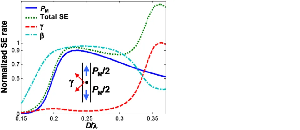
PM/2 PM/2
γγγγ
γγγγ PM Total SE β β β β D/λλλλ N o rm a li z e d S E r a te PM/2 PM/2γγγγ
PM/2 PM/2γγγγ
γγγγ PM Total SE β β β β D/λλλλ N o rm a li z e d S E r a teFig. 1(left). Normalized spontaneous emission rates of a radial dipole embedded in an infinite cylindrical GaAs (n=3.45) nanowire and located on the wire axis. Blue-solid curve: emission
PM into the HE11 fundamental mode. Dashed-red curve: emission rate γ into the other modes
including the radiative modes. Dotted-green curve: total emission rate, PM+γ. Dashed-dotted
curve: β-factor for the HE11 fundamental mode, β=PM/(PM+γ). Right: Scanning electron
micrograph obtained for a GaAs nanowire defined by e-beam lithography and reactive ion etching.
Figure 1 shows the main emission properties of a radial dipole located on the nanowire axis as a function of the normalized wire diameter D/λ. All the results are normalized by the emission of the same dipole placed in a bulk matrix of GaAs. The blue-solid curve represents the emitted photons that are directly coupled into the upward and backward fundamental HE11
modes. For an electric dipole located at r0 on the waveguide axis and oriented perpendicular
to the axis, the emission rate PM in a guided mode is analytically known [51],
PM = 1/8 ω2|p•ΕΕΕΕM(r0)|2, (1)
with ω the frequency, p the radial dipole momentum and EM the electric field of the guided
mode. The emission into other radiation modes, γ, is shown with the red-dashed curve, and the total emission (PM+γ) including the emission into the HE11 modes of interest is represented
with the green-dotted line curve. Interestingly, the total SE rate of the emitter is very close to its values in a bulk material. We additionally note that the fraction β=PM/(PM+γ) of the
photons that are directly emitted into the HE11 modes, defined as the β-factor and shown with
a dashed-dotted light-blue curve, remains above 90% over a wide diameter (or spectral) range. Unlike micropillars, this nearly-perfect coupling of the SE to a single-mode is obtained without implementing any cavity effect, but is simply due to the fact that, within the range of small diameters (150-300nm), the radiation out of our desired mode γ is negligible, see Fig. 1.
All these computational results are consistent with previous results obtained for related systems [37,49].
For a diameter of about D~0.22λ, the excellent emitter-mode coupling leads to a large β-value, β>0.95. This property is essential for implementing broadband S4Ps. However, the extraction efficiency remains limited for finite-size nanowires by the large divergence of the forward emission at the output facet [41,49,52] as well as by the photon escape at the bottom facet of the nanowire. As an example, GaAs nanowires standing vertically on a GaAs substrate -and containing a few InAs QDs- have recently been fabricated by electron-beam lithography and reactive ion etching. An extraction efficiency of around 17% has been measured in a preliminary photoluminescence experiment for such finite-size nanowires (8 µ m length, 250-nm diameter) [34]. In the next Section, we study these two basic effects, and present a simple FP model that accurately describes their impact on the efficiency of S4Ps.
Fig. 2. Fabry-Perot model for the emission of the dipole p in a nanowire of length L. A+ and A
-are the amplitudes of the upward and backward-propagating HE11 guided mode;rt and rb are
the reflection coefficients of the top and bottom facets. The emission rate in the continuum of radiation modes is denoted by γ. The transmitted intensity, T(θ), represents the fraction of the incident energy carried by the upward HE11 mode that is scattered by the top facet into a cone
defined by the angle θ.
3. Fabry-Perot model of the SE in finite-length nanowires
In finite-length nanowires, the SE rate of artificial atoms is modified by the reflections on the wire ends. The modification can be rigorously calculated by solving Maxwell’s equations for the whole scattering problem, a dipole source embedded in a finite-length nanowire. Unfortunately, such rigorous computations do not provide any physical insight and, as a consequence, they are only of little help for engineering and designing S4P devices. In this Section, we present a simple semi-analytical FP-model for the SE in finite-length nanowires. Like in earlier related works [26,53], the model assumes that the reflections on the ends only impact the emission rate into the fundamental mode; the emission into the continuum of radiation modes is assumed to be the same as in the infinite wire. In other words, this assumption allows separating the intricate problem of the emission in a finite-length wire into two independent and simpler problems: on the one hand the emission in an infinite wire, as described in Section 2, and on the other hand, the reflection of the fundamental mode on the top and bottom facets, see Fig. 2.
3.1. General formulae for Fabry-Perot resonators
The important physical parameters of the problem are defined in Fig. 2. In order to simplify the notations, without any loss of generality, we consider the case of a source located at the
centre of the nanowire, at a distance of L/2 of the bottom end. The unknown modal amplitudes of the HE11 mode in the forward and backward directions are respectively denoted by A+ and
A-. The amplitudes are coupled by the reflections at the top and bottom ends,
A+ = As + rb A-exp(iφ), (2a) A- = As + rt A+exp(iφ), (2b) where rt=Rt 1/2 exp(iφt) and rb=Rb 1/2
exp(iφb) are the top and the bottom reflection coefficients,
φ=2π/λneffL is the propagation phase of the HE11 mode over the length L (neff is the HE11
effective index) and As is the amplitude discontinuity induced by the dipole source. For radial
dipoles, the amplitude discontinuity is directly related to the SE rate into the fundamental mode and As=(PM/2)1/2. Solving Eqs. (2a) and (2b), one gets
A+ = As
( )
(
φ)
− φ + i r r i r 2 exp 1 exp 1 b t b , A- = As( )
(
φ)
− φ + i r r i r 2 exp 1 exp 1 b t t . (3)Like in a classical Fabry-Perot resonator, the impact of the multiple reflections is contained in the Airy function, the denominator in Eq. (3). If rt and rb are close to one, e.g. in a micropillar,
the Airy function is responsible for the frequency-selective enhancement of the SE in the cavity mode.
The total SE rate PT in the finite-length nanowire is calculated by balancing the power
escaping out and entering in a small box surrounding the dipole,
PT = (1-Rt)|A +
|2 + (1-Rb)|A
-|2 + γ . (4) Equation (4) evidences the main assumption of the model: the SE rate γ into the radiation modes is not affected by the wire ends; it is the same as that of infinitely long nanowires.
From the total SE rate PT, we can easily define the Purcell factor Fp defined as the
normalized SE rate into the cavity mode,
Fp = (1-Rt)|A +
|2 + (1-Rb)|A
-|2. (5)
In the context of S4Ps, it is also important to consider the extraction efficiency η(θ) of the finite-length nanowire, which we define as the fraction of emitted photons that are collected above the top facet in a cone with a solid angle 2π[1-cos(θ)] (see Fig. 2). Within the model scope, the number of photons collected into this cone is equal to T(θ)|A+|2, where T(θ) represents the fraction of photons transmitted into that cone when the top facet is illuminated by the upward-propagating HE11 mode. T(θ) is calculated by numerically solving the
scattering of the HE11 mode at the top facet, and then by applying a plane-wave
decomposition to the calculated near-field to determine the energy flow through the cone. The extraction efficiency is then given by
η(θ) = T(θ)|A+|2
/
PT . (6)The set of Eqs. (3)-(6) is so simple that it may appear to be only a rough and naive approximation. However, as will be shown in Section 6, comparisons with fully-vectorial computational data evidence that this set of equations can actually be used with confidence to analyse the photonic properties of S4Ps based on nanowires.
3.2. Specific case of null-reflectance top facets
In this work, we are interested in an efficient S4P that does not rely on any frequency-selective cavity effect. Our objective is to take advantage of the naturally large and broadband
β-factor of semiconductor nanowires (Fig. 1). The specific case of rt = 0, (no reflection at the
top facet) is of great importance, since the frequency-selective effect due to multiple reflections disappears. Equation (3) becomes,
A+ = As [1+rbexp(iφ)] and A
The total SE rate in the finite-length nanowire is thus simply given by the sum of the total emission rate in the infinite wire PM + γ and of an additional term resulting from the
interferences on the bottom facet,
PT = PM [1+|rb|cos(φ+φb)] + γ . (8)
In order to benefit from constructive interferences, the source has to be located on an antinode of the electric field, so that φ+φb=2mπ, m being an integer. In this case, the extraction
efficiency can be simply written as
η(θ) = 0.5T(θ) β(1+|rb|)2
/
(1+β|rb|). (9)It depends only on three physical parameters, T(θ), β, and |rb|. With this expression, one may
predict the efficiency of a single-photon source simply by studying three independent problems: (1) the reflection of the fundamental mode on the bottom facet, (2) its transmission through the top facet and (3) the emission in the infinite wire. Each problem constitutes a distinct building-block and the different blocks can be set together to design the S4Ps. Moreover, Eq. (9) shows that the efficiency is only limited by the β-factor of the infinite nanowire, provided that one engineers a bottom facet with a high reflectivity, Rb≈1, and a top
facet with a large transmission T(θ)≈1. This ideal situation provides an upper bound ηmax for
the extraction efficiency, ηmax=2β/(β+1). We have shown in Section 2 that a QD in a
semiconductor nanowire with a diameter D≈0.22λ exhibits a large β-factor (β>90%) over a broad spectral range. A 0.9 β-value corresponds to an upper bound ηmax≈95%.
We have assumed in this section that the emitter is located on the nanowire axis, and a detailed discussion of the role of the radial position of the emitter on its properties is beyond the scope of this paper. We note however that β does not depend critically on the radial position of the emitter [53]. For an in-plane polarized dipole closer to the nanowire axis than to the sidewall, values of β larger than 75% are expected. Furthermore, several approaches can be used to locate a single emitter on the nanowire axis, or very close to it. One example is the bottom-up synthesis of core-shell nanowires containing a single QD in the core [10]. Concerning top-down nanofabrication, various methods have recently been developed to control the location of single QDs within a PhC microcavity [25] or a micropillar [55]. Similar strategies could be applied to define a nanowire at the right place, once a QD has been selected within a dilute layer of self-assembled QDs.
In the next Sections, we design top and bottom facets, such that one reaches the upper bound of the extraction efficiency. In Section 4, we show that the top facet can be engineered by implementing a taper that efficiently converts the nanowire HE11 mode into a directive
beam. Then in Section 5, we discuss three different high-reflectivity mirror geometries.
4. Tapered top facet
In this Section, we focus on the scattering of the HE11 fundamental mode at the top facet of a
semi-infinite cylindrical nanowire. We first consider the simple case of cleaved facets, and then study how to improve the transmission T(θ) by introducing a cone-shaped tip (taper).
Figure 3 summarizes the main results obtained with the a-FMM. Figure 3a shows the facet reflection and transmission properties as a function of the normalized wire diameter D/λ. T(θ=π/2) represents the total fraction that is scattered upward. T(θ) is shown as a function of θ in Fig. 3b for several values of D/λ. For D=0.22λ, our target diameter value for achieving a large β, the performance of the cleaved facet is rather poor. As we show in Fig. 3a, the transmission of the HE11 mode (dashed-green line) for θ=π/2 (NA=1) is only 63% (it is as
small as 37% for NA=0.75), since the modal reflectivity Rm (blue-dotted line) is 24% and the
backscattered intensity Rs (solid-red line) in radiation modes is as large as 13%.
Nevertheless, an interesting outcome of these calculations is that, as we decrease the diameter, the transmission dramatically increases (Fig. 3a) and the beam divergence decreases (Fig. 3b). This dual property is very important for engineering inverse tapers that efficiently
couple light by adiabatically tapering the nanowire to a small diameter supporting a mode mostly in air [38-42]. In such a structure, the effective refractive index gradually decreases, which minimizes back-reflections and reduces the beam divergence in air.
(a) (b) Rm Rs T (a) (b) Rm Rs T
Fig. 3. Optical properties of cleaved facets. (a) Dotted-blue curve: modal reflectivity Rm.
Dashed-green curve: transmission Τ(θ=π/2) of the fundamental HE11 mode for a collection
with a numerical aperture of 1. Solid-red curve: intensity Rs reflected into the radiation modes.
All the coefficients are shown as a function of the normalized wire diameter D/λ. (b) T(θ) (in units of π) for different values of D/λ.
htip D Rs T Rm Dtop (a) (b) (c) (d) htip D Rs T Rm Dtop htip D Rs T Rm Dtop (a) (b) (c) (d)
Fig. 4. Right inset: tapered nanowire geometry with its physical parameters, htip, Dtop and D.
Left panel: (a) Transmission of the fundamental mode HE11 as a function of θ for a diameter of
D=0.22λ. (b) Modal reflectivity Rm. (c) Transmission of the fundamental HE11 mode for
θ=π/2 (ΝΑ=1). (d) Intensity Rs back-scattered into the radiation modes. All results are obtained
for λ=0.95 µm and for Dtop=155 nm. The solid-blue and dashed-green curves are obtained for
htip=1 µm and htip=2 µm, respectively.
In order to improve the collection efficiency of the HE11 mode, we introduce a
cone-shaped tip (see the right inset in Fig. 4). The HE11 guided mode, well-confined at the bottom
of the tip, becomes less and less confined as the wire narrows to its top diameter,
Dtop=155 nm, a value chosen from Fig. 3 because it both decreases the angular divergence of
the output light and minimizes the radiation backscattering loss. Note that the smaller the top diameter, the better the tip performance. However, small top diameters requires a large tip height (noted htip in the inset in Fig. 4) in order to maintain adiabaticity as the photons
propagate in the tip.
Figure 4 summarizes the main optical performances of a tapered tip with a top diameter
performed for λ=0.95 µm, a wavelength that is typical for the emission of InAs/GaAs self-assembled QDs. The adiabatic transition dramatically improves the optical properties of the output end of the nanowire, for a targeted nanowire diameter D=0.22λ at the QD location : the modal transmission reaches a value as large as 99%, with only 0.6% (resp. 0.2%) of back-radiation loss and 0.13% (resp. 0.095%) of specular reflectance for a tip height of 1 µ m (resp. 2 µm). The collection efficiency (Fig. 4a), which exceeds 96% for NA=0.75 and for a 2 µ m-height tip, is now very attractive for S4P applications. Moreover, the tip is expected to allow broadband operation, as will be demonstrated in Section 6. From a technological point of view, the feasibility of such long and sharp tips has been demonstrated for the growth of core-shell nanowires [10-11] as well as for the top-down nanofabrication of wires using focused ion beam etching [41].
5. Bottom mirror
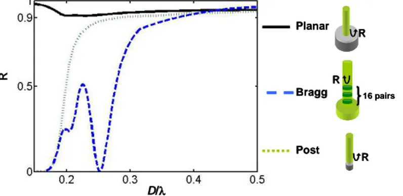
5.1 Bragg, Post and Planar geometries
In order to efficiently redirect the photons emitted toward the substrate, we have studied several possibilities for designing reflecting facets, pursuing high reflectivity over a broad spectral interval. Details concerning the design have been recently published [43], and we just intend to summarize the main results hereafter (see Fig. 5).
We first consider dielectric Bragg mirrors embedded within the wire, as suggested by [54] in the context of nanowire lasers. The dashed-blue curve in Fig. 5 shows the reflectance of quarter-wave-stack GaAs/AlAs (n=3.45/2.95) Bragg mirrors composed of N=16 pairs and connected to the GaAs substrate. For the calculation, performed at a fixed wavelength (λ=0.95 µm), each layer of the reflector is assumed to have a quarter-wave optical thickness for every diameter D, implying that, as D varies, the layer thicknesses also vary. For instance, the GaAs layers are λ/(4neff)-thick, neff being the effective index of the HE11 mode of a GaAs
wire of diameter D. The dielectric mirror performances are very poor for our targeted diameter D=0.22λ, the reflectivity being even nearly null for D=0.25λ. It only rises up for
D/λ>0.3.
Pursuing alternative ways to achieve high reflectance, we have considered wire facets connected to a metallic planar silver mirror. The reflectivity of such a mirror exhibits a pronounced dip with a minimum reflectivity (R<1%) for D/λ=0.19, due to the coupling to the surface plasmon polaritons of the metal [43]. The suppression of this plasmonic effect can be achieved by coating the mirror with a thin silica adlayer (n=1.5), see the right inset in Fig. 5. The solid-black curve in Fig. 5 is obtained for an optimized adlayer thickness of 9 nm, and shows a flat reflectance that remains high for any wire diameter (R=91% for D/λ=0.22).
D/λλλλ R 16 pairs R 16 pairs R R Planar Planar Bragg Bragg Post Post R R R
Fig. 5. HE11 modal reflectance R of the three different mirror geometries as a function of the
diameter D for λ=0.95 µm. The geometries are: a planar silver mirror covered by a 9-nm-thick dielectric (n=1.5) adlayer (solid-black curve), a post silver mirror covered by the same adlayer (green-dotted curve) and a 16-pair quarter-wave-thick GaAs/AlAs Bragg mirror connected to a GaAs substrate (dashed-blue curve).
Finally we consider a metallic post-mirror geometry [43]. Such compact mirrors might prove more practical and versatile than planar ones, especially for nanowires obtained using a bottom-up fabrication process [29,43]. A low reflectance (dotted-green curve) is observed for small diameters, for which the HE11 field is only weakly confined and therefore weakly
interacts with the metallic post. However, the post geometry offers high reflectance (R>80%) for D>0.26λ, or even for D>0.22λ provided that a 9-nm-thickness adlayer (n=1.5) is inserted between the GaAs wire and the metallic post. For this optimal thickness, a 0.9-reflectance is achieved for diameters as small as 0.28λ.
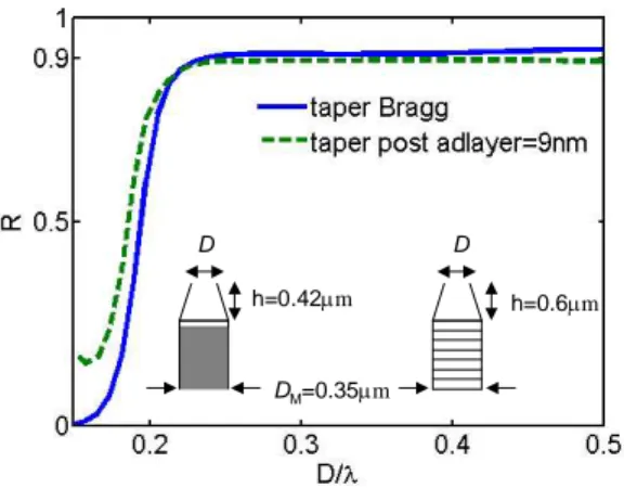
5.2 Tapered mirror
As seen in Fig. 5, for small diameters, the reflectance of Bragg mirrors is rather poor, and that of post mirrors, although more promising, suffers from a drop and does not reach a plateau value until D/λ>0.3. Clearly, these two geometries are not optimal for our targeted diameter
D=0.22λ. However, the reflectivity of the Bragg and post mirrors both increase dramatically
for larger diameters, D/λ>0.3. This implies that a taper could be used to enlarge the bottom extremity of the wire in order to improve the mirror reflectance, as sketched in the insets of Fig. 6. Using such a taper, one can combine an optimal SE coupling to the guided mode for
D/λ=0.22 and a high modal reflectance on a dielectric or metallic mirror.
With the a-FMM, we have optimized the taper heights, bearing in mind that large heights are indeed beneficial for an adiabatic mode transformation, but are challenging for the fabrication. We found that h=0.6 µm for the Bragg mirror and h=0.42 µm for the post mirror are two reasonable values enabling a good compromise. The performances of the tapered mirrors are shown in Fig. 6. Indeed, these tapered mirrors outperform those previously designed without tapers. Importantly, we find that a high modal reflectivity, R=89%, is obtained for the Post and Bragg geometries, for the targeted value of D=0.22λ.
h=0.6µm h=0.42µm D D DM=0.35µm h=0.6µm h=0.42µm D D DM=0.35µm h =0.42D=0.35 Ag
Fig. 6. HE11 modal reflectance R of the Bragg and Post geometries with a tapered section
inserted between the wire end (diameter D) and the mirror section (diameter DM=0.35 µm), as a
function of the diameter D. The calculations are performed for λ=0.95 µm. The solid-blue line shows the reflectance of a 16-pair quarter-wave GaAs/AlAs (n=3.45/2.95) Bragg mirror with a taper height of 0.6 µm. The dashed-green line shows the reflectance of a post silver mirror covered by a thin dielectric adlayer (n=1.5) of 9-nm thickness adlayer with a taper height of
h=0.42 µm.
6. Design validation: extraction efficiency of single-photon sources
In the previous Sections 4 and 5, we have designed out-coupling tips and mirrors that efficiently manage photons at the wire extremities. In this Section, following the Fabry-Perot model predictions, we combine these results and design three efficient single-mode S4Ps operating around λ0=0.95 µm. All designs rely on the GaAs nanowire studied in Section 2
with Dtop=155 nm and htip=1 µm. By combining this taper design with the three
high-reflectivity bottom mirrors that have been engineered in the previous Section, three different possible S4P designs are straightforwardly obtained. The three devices are labeled accordingly to the geometry used for the bottom mirror: Planar, Post and Bragg. Figures 7(a), 7(d) and 7(g) show the three S4P structures. It is noteworthy to mention that, because of the 16 pairs needed in the Bragg mirror in order to obtain a good reflectivity, the Bragg S4P is 3 times taller (≈5 µm-height) than the Planar and the Post S4Ps (≈1.5 µ m-height).
Fig. 7. Intensity distribution |Ex|2, normalized SE rate PT and extraction efficiency η for the
three S4Ps built with the same top end but with different bottom mirrors. (a), (b) and (c) Planar S4P. (d), (e) and (f) Post S4P. (g), (h) and (i) Bragg S4P with 16 pairs in the dielectric mirror. The QD locations correspond to the intensity maximum (in the center of the white cloud). In (b), (e) and (h), the Fabry-Perot model predictions (red-solid line), the a-FMM calculation data (blue circles) and the Fabry-Perot model predictions with rt = 0 (black-dashed line) are shown.
In (c), (f) and (i), the extraction efficiency has been calculated for θ=60° and θ=45° with the Fabry-Perot model (red- and black-solid curves) and with the a-FMM (red squares and black circles).
Once the bottom and top extremities are designed, according to the Fabry-Perot model developed in Section 3, only the nanowire-section length L and the vertical QD location along the nanowire-axis have to be determined to complete the design. For the sake of simplicity, we have decided to locate the dipole source on the nanowire axis, at a distance L/2 of the bottom mirror and of the taper tip. The choice is rather arbitrary, but the exact vertical location of the QD on the nanowire axis is not a sensitive parameter of the design, as long as the QD is located at an antinode of the electric field. Then, the length L of the nanowire is chosen by fulfilling the phase-matching condition φ + φb=2mπ at λ=λ0, see Eq. (8). We obtain
L=192, 106 and 514 nm for the Planar, the Post and the Bragg geometries, respectively. Note
that the phase φb of the bottom reflection coefficient is defined at the end of the nanowire,
which means at the top of the bottom taper where D=0.22λ0 in the Post and the Bragg cases.
The designs are validated by calculating the emission of a QD in the whole structure with the a-FMM as a function of the wavelength λ and by comparing these fully-vectorial computational data with the Fabry-Perot model predictions. Figures 7(a), 7(d) and 7(g) show the electric-field intensity distributions |Ex|2 in arbitrary units. The total SE rates of the QD,
normalized by the SE rate in the bulk material, are shown in Figs. 7(b), 7(e) and 7(h). The predictions of the Fabry-Perot model (red-solid curve) are in very good agreement with the fully-vectorial computational data (blue circles) obtained with the a-FMM. This agreement validates the model, which can be used to analyse finely the physical mechanisms responsible for the SE modification. The black dashed curves correspond to the Fabry-Perot predictions given by Eq. (7), which are obtained by assuming a null reflectivity for the tip, rt=0.
The Planar and the Post cases present a clear cosine shape, which evidences the interference effect on the bottom mirror. For the Post geometry, the fringe period is smaller than that of the Planar geometry, because the phase φb varies more rapidly as a function of the
wavelength. Moreover, the interference effect disappears for λ>1.05 µm essentially because the bottom reflectivity Rb of the tapered post mirror drops below 50%. Indeed, for long
wavelengths, this mirror does not perform well. The SE rate of the Bragg S4P does not exhibit any interference effect because the band-gap of the Bragg mirror is too narrow. The predictions of the Fabry-Perot model, given by Eq. (4), are in quantitative agreement with those given by Eq. (7), except for λ<0.9 µm. At these short wavelengths, the tip reflection increases (Rt > 5%) and the impact of the multiple reflections becomes visible as a
superimposed oscillatory behaviour with a high frequency.
The S4P efficiencies are shown in Figs. 7(c), 7(f) and 7(i) for two collection angles,
θ = 45° (NA=0.7) and θ = 60° (NA=0.87). Let us recall that the extraction efficiency is
defined as the fraction of emitted photons that are collected in a cone with an angle θ, see Section 3. The predictions of the Fabry-Perot model are presented by the red and black-solid lines and the results of the fully-vectorial a-FMM calculations are presented by the red squares and the black circles. As expected, the three S4P designs provide a high and broadband extraction efficiency. For a numerical aperture NA=0.87, the efficiencies of the Planar and the Post S4Ps are larger than 90% over a remarkably broad spectral range
∆λ=70 nm, with a maximum reaching 94%, see Figs. 7(c) and 7(f). The performances of the
Bragg S4P are only slightly below, η>85% for ∆λ=26 nm with a maximum reaching 90%. This is due to the spectrally selective nature of the Bragg mirror and to its lower reflectivity. The latter could be increased by considering a higher number of pairs.
7. Discussion: which applications for single mode nanowire S4Ps?
We briefly discuss here the potential applications of photonic wire QD-S4Ps, by comparing their assets and drawbacks versus S4Ps based on the Purcell effect, and more specifically micropillar-S4Ps.
In terms of S4Ps performance requirements, the most demanding application is quantum computing with single photon Qubits [3]. Whereas a high degree of photon indistinguishability is needed to ensure a high fidelity of quantum logical gates, the S4Ps should also emit on demand a single photon in the optical channel with a very high probability
(>99%), in order to ensure the scalability of the quantum computer. Efficient sources of indistinguishable single photons are more generally necessary for all quantum information processing schemes relying on two-photon interference, such as quantum teleportation or post-selective production of polarization entangled photon pairs [12]. Experimentally, the generation of largely indistinguishable single photons (i.e. displaying a wave-packet overlap around 80%) has been demonstrated for a single QD embedded in a micropillar [12] or PhC [5] microcavity. Such experiments are performed at low temperature under quasi-resonant optical excitation, so as to reduce as much as possible the magnitude of decoherence processes; the Purcell effect is also used to speed up the radiative exciton recombination, and further decrease the relative impact of decoherence processes on emitted photons. Although desirable, the Purcell effect is not strictly necessary to ensure single photon indistinguishability. For instance, short radiative lifetimes and radiatively-limited exciton dephasing (at 5K under resonant optical pumping) has been reported for giant-oscillator strength InGaAs/GaAs QDs prepared by thermal annealing [56]. The insertion of such QDs inside GaAs photonic wires appears therefore as a promising route toward bright sources of indistinguishable photons.
In the context of quantum key distribution (QKD), several communication protocols – based e.g. on polarization encoding - do not require single photon indistinguishability. Present commercial QKD systems implement a coherent source, which is strongly attenuated in order to reduce the number of multi-photon pulses. In the context of QKD, bright S4Ps delivering on demand a single photon in the optical channel with a high probability (η~1) are highly desirable, since they would permit increasing the maximum channel length for secure transmission and/or the bit rate [13]. As shown in Section 6, S4Ps based on a single QD in a nanowire are likely to reach extraction efficiencies of the order of 90%, well above the best values reported to date for pillar microcavities (~40% [6-7]). Interestingly, a collection optics with numerical aperture of NA~0.4 is enough to collect properly the emission beam of a micropillar (d>1 µm), whereas a larger NA (NA~0.7-0.8) is needed in the case of nanowires. In both cases, some adaptative optics is needed to couple the emission beam to a single-mode fiber (NA~0.1).
Compared to micropillar S4Ps, which exploit coupling to a high Q cavity mode, the performances of nanowire S4Ps should be less sensitive to technological imperfections such as sidewall roughness. However, the nanowire geometry displays also some potential drawbacks. First of all, the QD exciton radiative lifetime is longer in a nanowire than in a micropillar in the Purcell-enhancement regime, which puts a lower limit on the maximum repetition rate of the QD-S4Ps. Secondly, the Purcell effect can also be used to ensure a linear polarization of the QD emission in asymmetric micropillars [14]; this is interesting for QKD since the single photons must be prepared in a well defined reference polarization state, prior to polarization encoding. These drawbacks of nanowire-S4Ps can be at least partially cancelled by playing with the emitter itself. As already mentioned, the dynamics of the QD exciton can reach the 100ps range for giant-oscillator strength InGaAs or GaAs QDs [56]. Furthermore, a linear polarization degree of the exciton line as high as 90% has been observed for particular InAs/GaAs QDs selected within very dilute assemblies [57].
Let us finally note that the photonic wire geometry is obviously attractive when optical microcavities and photonic crystals are either not available or difficult to build, or when the single photon emitter has a large emission bandwidth. For instance, II-VI [58] and GaN/AlN [59] QDs are able to emit single photons at temperatures close to 300K (thanks to the larger magnitude of the exciton-biexciton splitting in these QDs), but their emission lines are severely broadened (∆λ ~ 10-20 nm) due to the exciton-phonon coupling. Another important example is colour centres in diamond, which operate at 300K but also display broad emission lines [60-61]. In both cases, embedding the single-photon emitter inside a nanowire antenna is a very attractive approach for ensuring a single-mode emission and efficient photon collection.
8. Conclusion
In summary, we have designed three different efficient single-mode single photon sources by exploiting the unique radiation properties of QDs embedded in cylindrical GaAs nanowires. In particular, we have been able to combine metallic, dielectric and semiconductor materials to overcome several limitations and to design very small antennas that are capable of efficiently funnelling the emission of a nanosource into a single mode. Referring to the Post and Planar geometries in Figs. 7a and 7d, it is noticeable that the antenna volume is of the order of 0.05
λ3. In addition, in contrast to recent optical nanoantennas based on plasmonic effects [62-63], our approach does not rely on any resonance effect and the funnelling is actually achieved over a very broad spectral range.
For the best geometry (planar metallic mirror), the extraction efficiency is larger than 90% over a broad spectral range of 70 nm @ λ0=0.95 µ m. Our designs fully remove the energy
matching condition between the QD and the resonant wavelength, which is classically needed in microresonators. Therefore, such designs open the way to the fabrication of efficient single-mode S4Ps using a non-monochromatic single photon emitter, such as a colour centres in diamond at 300K, or semiconductor QDs at moderate temperature (T>100K).
Acknowledgments
The authors gratefully acknowledge fruitful discussions with G. Lecamp, who was involved in this research during his PhD. They also acknowledge B. Gayral and I. Robert-Philip. The work at Institut d’Optique has been performed under the NanoEPR project of the 2006 NanoSci-ERA European programme. JMG and JC acknowledge support from the IST-FET European project QPhoton, as well as discussions with N. Gregersen, R.T. Nielsen and J Mork (DTU Copenhaguen).