Comprehensive Dynamic On-Resistance Assessments in GaN-on-Si MIS-HEMTs for Power Switching Applications
Po-Chien Chou1†, Ting-En Hsieh2†, Stone Cheng1,*, Jesús A. del Alamo3, Edward Yi Chang2.
1. Department of Mechanical Engineering, National Chiao-Tung University, No. 1001, University
Road, Hsinchu 30010, Taiwan;
2. Department of Materials Science and Engineering National Chiao-Tung University, No. 1001,
University Road, Hsinchu 30010, Taiwan;
3. Microsystems Technology Laboratories, Massachusetts Institute of Technology, Cambridge, MA
02139 USA;
* Corresponding Author: stonecheng@mail.nctu.edu.tw
† These authors contributed equally to this work Abstract
This study comprehensively analyzed the reliability of trapping and hot-electron effects responsible for the dynamic on-resistance (Ron) of GaN-based metal–insulator–semiconductor (MIS) high electron mobility transistors (HEMTs). Specifically, this study performed the following analyses. First, we developed the on-the-fly (OTF) Ron measurement to analyze the effects of traps during stress. With this technique, the faster one (with a pulse period of 20 ms) can characterize the degradation, the less the de-trapping affects the current collapse recovery. Then, dynamic Ron transients were investigated under different bias conditions, including combined off state stress conditions, back-gating stress conditions, and semi-on stress conditions, in separate investigations of surface- and buffer-, and hot-electron-related trapping effects. Finally, the experiments showed that the Ron increase in semi-on state is significantly correlated with the high drain voltage and relatively high current levels (compared with the off-state current), involving the injection of greater amount of hot electrons from the channel into the AlGaN/insulator interface and the GaN buffer. These findings provide a path for device engineering to clarify the possible origins for electron traps and to accelerate the development of emerging GaN technologies.
I. INTRODUCTION
The GaN properties and heterojunction technologies of GaN power HEMTs now enable high voltage (over 650 V) [1,2], high power density (35 W/in3) [3], high frequency (over 1 MHz) [3], and high
temperature (up to 200 °C) operation [4]. Therefore, they can be used to improve power conversion in energy-efficient, smaller and more cost-effective products, such as power supplies, hybrid electric vehicles/electric vehicles (HEV/EVs) [5,6], and photovoltaic (PV) inverters [7]. Nevertheless, a relatively large amount of intrinsic defects and impurities still exist in the grown AlGaN/GaN hetero-structures which may act as charge traps (possibly causing the current collapse and increase in dynamic
on-resistance Ron), and which thereby undermine the dynamic performance [8-10]. In more mature
lateral GaN technology, dynamic switching problems still present a limitation on the market penetration of these devices. Several papers investigated the time resolved dynamic Ron transients
performed in off-state and back-gating stresses, suggesting the unique dominant trapping mechanisms related to the surface and to GaN buffer [11-13]. Conversely, systematic descriptions of the correlation of hot electrons-related charge-trapping and surface-state creation for devices stressed in semi-on state are rarely reported in the literature [14,15]. Hot electrons-related charge-trapping play a major role in increasing the dynamic Ron and promoting significant parasitic trapping effects (critical in hard
switching conditions).
Therefore, this study comprehensively analyzed the main reliability concern for charge-trapping mechanisms in GaN-based MIS-HEMTs. The on-the-fly technique is proposed to characterize trapping transients (increase in Ron over time) for devices submitted to different bias regimes. This methodology
is based on combined off state stress conditions, back-gating stress conditions, and semi-on stress conditions for separately investigating the surface- and buffer-, and hot-electron-related trapping processes. This study identified and described the dominant trapping mechanisms affecting the dynamic Ron: (i) in the off state condition, the trapping at the surface and in the buffer is promoted by
high drain–gate bias (VDG), (ii) in the back-gating condition, the trapping mostly occurs in the buffer,
without any significant surface effect and is promoted by high vertical drain-to-substrate potential, (iii) in the semi-on condition, the injection of hot electrons from the channel into the AlGaN/insulator interface and the GaN buffer is caused by high drain voltage (VDS) combined with high drain current
(IDS). These findings provide a path for device engineering to minimize degradation of dynamic
on-resistance and to mature GaN into the robust technology.
Keywords: GaN MIS-HEMT, reliability, trapping related degradation, failure mechanisms, hot electrons, dynamic RON.
II. DEVICE DESCRIPTION
Figure 1 shows a schematic illustration of the AlGaN/GaN HEMT heterostructures used in this study. These devices were fabricated using a complete CMOS-compatible process for GaN-based MIS-HEMTs on a 150-mm p-type Si substrate. The structure has a 3.9 µm-thick GaN/AlGaN buffer layer, a 2.1 µm-thick GaN channel layer, a 20 nm-thick Al0.23Ga0.77N barrier layer, and a 4 nm-thick GaN
capping layer. A 50 nm-thick Si3N4 film was deposited by plasma-enhanced chemical vapor deposition
(PECVD) and deployed as the gate insulator. The Ohmic contacts were formed by Ti/Al-based metallization, while Ni-based metallization for the gate contact and both are defined by means a lift-off process. Details on the Ohmic and gate contacts formation can be found in Refs. [16] and [17], respectively. To clarify the origin of the degradation mechanism, the tested devices have no field plate (that has been proven to mitigate the large fields at the gate-drain and gate-source).
(a)
(c)
(d)
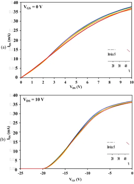
Fig.2. Representative device characteristics of MIS-HEMTs (five devices) used in this work.(a) Output (VGS = 0 V) characteristics measured at VDS from 0 V to 10 V; (b) transfer (VDS = 10 V)
characteristics measured at VGS from -25 V to 0 V; (c) drain-leakage (IDoff) characteristics measured at
VDS from 0 V to 100 V; (d) Gate-leakage breakdown (IGoff) characteristics measured at VDS from 0 V to
100 V. Negligible permanent degradation takes place as a result of the entire device characterization. All devices were fabricated on the same 4-inch wafer and in close proximity to each other. Before starting with the evaluation of the origin of dynamic Ron, an initial survey of reliability qualification
was performed to screen out early-stage degradation. These HEMT devices were preliminary subjected to direct current (DC) current-voltage (I-V) and off-state breakdown analyses with the aim of separating permanent degradation from trap-related phenomenon before any stress. Figures 2(a) and 2(b) show the representative results obtained from five identical samples. Characteristics of drain current (IDS) versus drain voltage (VDS) and gate voltage (VGS) were recorded to determine the main DC
device figures of merit (FOMs), such as the linear-regime drain current IDlin (measured at VGS
= 0 V and VDS = 1 V), maximum drain current IDmax (measured at VGS = 0 V and VDS = 10 V),
mA for VDS = 1 V) [18,19]. Figures 2(c) and 2(d) show the drain and gate leakage currents (IDoff and
IGoff) measured in the voltage range from VDS = 0 V to 100 V with VGS = −25 V (off-state).As can be
noticed, the fabricated devices are able to sustain large drain biases (VDS >100 V) without the onset
of a sudden increase of leakage current. Approximately 40 devices were evaluated and sorted to obtain well-matched I-V characteristics.
Fig.3. Time evolution of Ron and IDmax (normalized to their initial values) and IGoff during the devices are
on-stressed at VDS = 20 V and VGS = 0 V. Small degradation in Ron and IDmax, less than 10%, occurr
Fig.4. (a) Output (VGS = 0 V) and (b) transfer characteristics (VDS = 10 V) before and after on state
stress. Negligible permanent Ron and IDmax happen.
Permanent and recoverable trapping and de-trapping effects may lead to significant increase in dynamic Ron. In order to clearly identify the effects on device characteristics, we have stressed these
devices in the on state with VDS = 20 V and VGS = 0 V at room temperature which generates a constant
heat into channel [9]. This is a harsh stress bias condition designed to accelerate the degradation rate and eventually permanent degradation in Ron. During stress, we have characterized several device
parameters by a benign characterization suite for a period of 300 seconds each. Figure 3 plots the time evolution of Ron and IDmax (normalized to their initial values) as well as IGoff as a function of stress time
for the device that has been subject to 40000 seconds. The device shows quite robust characteristics, during and after on state stress test, no sudden increase in gate leakage (IGoff) is observed. In order to be
able to separate permanent from trap-related degradation, the devices are exposed to ultraviolet illumination to fully de-trap the captured charge after stress [20,21]. As Fig. 4 shows, the samples exhibit very minor degradation in their Ron and IDmax values, permanent degradation will still be small
and its effect on device characteristics can be negligible.
III. ON-THE-FLY RON CHARACTERIZATION
A reliable and reproducible performance assessment of MIS-HEMT technology must be benign in that it must produce reliable and must not cause damage or irregular current behaviors. For this, the measurement conditions have to be selected carefully, so that the transient trapping/de-trapping effects can be studied in detail. The increase in dynamic Ron is carried out by means of on-the-fly (OTF)
transient characterization [22-24]. This technique is proposed to monitor the drain current (IDS)
degradation in stressed devices under off-state conditions. The main advantage of this technique is that the dynamics of trapped charge in transistors can be captured very shortly after the stress is removed.
(a)
(b)
Fig.5. (a) The on-the-fly Ron characterization involves holding a small bias on the drain and sampling
the drain current continuously. This technique allows a few point sweep to be completed and the stress conditions returned in time interval of 20 ms. (b) the recorded Ron transient is obtained by continuously
switching the device between on-state (VDS = 1 V, VGS = 0 V, in linear region) and off-state (VDS = 20
V, VGS = -25 V for safety reason) fordifferent periods of stress times (1 s, 5 s, and 10 s for each cycle).
The analysis is performed in an on-wafer probe station equipped with thermal chuck that allows device characterization through external test equipment (two Keithley 2636B Source Meters). Figure 5(a) is a schematic diagram of the experimental procedure for OTF Ron transient characterization. Devices are
kept in a defined trapping condition for 1000 s (for reliability assessment in different operating bias conditions, Section IV); Stress-induced change in Ron is evaluated by repeatedly biasing the device with
short pulses (20 ms). Device Ron is evaluated by averaging the sampled IDS values obtained from the
measurement time interval (between 4 ms and 20 ms), retains sufficient accuracy to capture the transients. To further clarify the dynamic behavior, the correlation between specific trap formation and stress time for each cycle have been established to investigate the de-trapping effects during the
characterization. Figure 5(b) shows the Ron transients, which consist of a series of stress pulses with
different stress times (1 s, 5 s, and 10 s) applied to a single device, and the change in Ron between pulses. During this measurement, the device is kept in the off-state bias (VGS = − 25 V, VDS = 20 V, and
VSUB = 0 V) for a long time (1000 s). Interestingly, a weak dependence of Ron on the time the device is
held in the OFF state; these pulses are significantly shorter than the de-trapping time of the defects. The Ron did not substantially differ. Therefore, the device does not change its stress sequence (stressed
1 s for each cycle) during the short measurement pulse; this guarantees a reproducible and reliable evaluation of the Ron time transients.
IV. TRAPPINGMECHANISMSIN GAN-BASED MIS-HEMTS
Fig.6. Schematic representation of the possible trapping mechanisms of increased RON in MIS-HEMTs
exposed to high drain bias: electron trapping at both the surface (due to the electric field in the drain-gate access region) and in the buffer (due to the high vertical field from the drain directed towards the substrate).
(b)
Fig.7. (a) RON increase when the device was continuously pulsed under off state drain bias stresses;
samples were subject to varying high drain-bias stress from VDS = 20 to 100 V at VGS = - 25 V. (b)
Time-constant spectra for RON transients. A sum of exponential terms is used to fit the measurement
data. High drain bias substantially increased the magnitude of transients with the related time constants (10-100 s).
Operation of the fabricated devices at a high drain bias increased Ronover time. Figure 6 shows the
schematic drawing of lateral and vertical trapping phenomena in MIS-HEMTs exposed to high drain bias. The increase in Ronoriginates from increased injection of electrons from the gate-drain access
regions (due to the high negative gate-drain voltage) and from the substrate to the buffer (due to the flow of drain-bulk vertical current). The physical origin of the mechanisms responsible for dynamic Ron
was investigated by analyzing trapping transients on devices starting at various quiescent bias points in the off-state, from VDS = 20 V to 100 V in 20 V increments at VGS = - 25 V, as shown in Fig. 7(a).
When the evolution of normalized Ron was reported as a function of time, an increase in stress voltage
accelerated the trapping process and resulted in a stronger Ron increase. These results suggest that the
phenomena causing the Ron temporary increase during time might be related to electron capture
processes. Figure 7(b) reports the time constant spectra [25] extracted from Ron transients in Fig.7(a):
the time constants are extrapolated by fitting the curves based on a stretched exponential function (black solid line in Fig. 7(a)); the derivative spectrum (dRon/dlog(t) waveform) for each tested has a
clear peak, with relatively slow time constant (in the time interval of 10–70 s) [11,13]. Remarkably, increasing drain potential yields a dramatic decrease in the time constant associated with the transient response.
Fig.8. Schematic representation of the possible trapping mechanisms responsible for RON-increase in
MIS-HEMTs exposed to negative substrate bias (Vsub): the increased injection of electrons from the
substrate to the buffer (due to the high vertical field).
(a)
(b)
Fig.9. Recorded Ron transients (a) and associated time constant spectrum (b) obtained from different
dynamic Ron also increases, but the time constants do not significantly differ from those in Fig. 5(b). A
clear positive peak appears in the said time constant signals.
The increased injection of electrons from the Si substrate to the buffer has a critical interaction with the performance and reliability of said devices. Mostly deep traps have been associated with early stages of degradation. Therefore, the effects of trapping in the buffer must be studied carefully. Furthermore, the back-gating measurement provides an effective method to distinguish between the surface- and buffer-related traps; this technique could offer a good indicator for process improvement. Figure 8 shows the devices stressed under back-gating bias at different negative substrate voltages (VSub = −20
to −100 V with -20 V increments), with grounded source, gate and drain. The main mechanism of degradation is trapping in the buffer (high vertical field between the channel and substrate), with negligible surface trapping (lateral field is zero between the three terminals) [26].
Dynamic Ron measurements at different back-gating stress have been performed with the goal of
clarifying the physical origin of these transients. Figure 9 shows Ron transients and related time constant
spectrum with different back-gating biases (Vsub) from -20 V to -100 V in -20 V step. As VSub increases,
Ron increases exponentially over time. The time constant spectrum has a clear peak with a time constant
in the range of 10–50 s. The dynamic Ron increases in the devices presumably resulting from a
depletion region forming within the GaN buffer. Also, electrons can be injected from the substrate to the buffer, eventually being trapped either in the buffer or in the GaN channel layer.
Substrate bias experiments are key performance indicators for distinguishing between surface- and buffer-related trapping processes. Notably, during back-gating stress,Ron increases by approximately a
130 % within the first 100 s of operation at 100 V and then flattens out. Under off state stress, however, it shows a continuous increase in stress but does not saturate. The probable explanation for this behavior is that the surface traps have a larger effect on transient Ron characteristics compared to
buffer traps.
Fig.10. Schematic representation of the additional possible trapping mechanisms responsible for the “semi-on state” RON-increase in MIS-HEMTs exposed to high drain bias: the injection of hot electrons
(a)
(b)
Fig.11. (a) Time-resolved Ron transients acquired with constant quiescent VDS (60 V) and multiple
quiescent VGS (VTH - 5 V to VTH + 1 V), in comparison with Ron transient measured at quiescent bias
point (VDS = 100 V, VGS = VTH + 1 V; red line) to further characterize the hot-electron effects.Dynamic
Ron increase worsen as VGS > VTH. (b) During semi-on stresses, analysis of time constant waveforms
showedan additional trap peak (in the time interval of 100–1000 s), which suggested a hot-electrons-related trapping mechanism.
This study also investigated the trapping mechanisms induced by the exposure to high semi-on state bias; it is important to evaluate the impact of the injection of hot electrons from the 2DEG into trap states to assess the stability of the devices. The semi-on bias condition is typically the worst case for hot-carrier stress. Notably, the additional traps filled in the semi-on condition are not present in off-state condition; strong correlation with hot-electron effects (see the schematic drawing of the trapping behavior in Fig. 10). When the device is biased in the semi-on state under a high current flow and high
drain bias, electrons are accelerated by the field and then injected in the (SiN/AlGaN) interface and buffer near the channel.
This study further investigated the effects of hot electrons on device reliability. Ron transients and
related time constant spectra have been acquired by keeping the quiescent drain bias (VDS = 60 V)
constant and by sweeping step-by-step the quiescent gate bias from VGS = VTH - 5 V (off-state) to VTH +
1 V (semi-on state)
.
Further, we also carried out experiments under a higher a quiescent bias point (VDS= 100 V, VGS = VTH + 1 V) to investigate an increase of hot electron concentration.
Figure 11(a) shows that dynamic Ron does not significantly change when exposed to the off-state
quiescent bias (VGS < VTH). However, when the devices are biased in the semi-on state quiescent bias
(VGS > VTH), the Ron increase during semi-on (220% at VDS = 100 V and VGS = VTH + 1 V) is higher than
during off-state (160% at VDS = 60 V and VGS = VTH - 5 V). The Ron increase in the semi-on state is
significantly correlated with the drain current. This suggests an additional trapping mechanism that is promoted by the high voltage (VDS) and relatively high current levels (compared with the off-state
current).
To ensure that the observed phenomenon only occurred in semi-on state operation, and to identify the possible trapping mechanism emerges, involving the injection of hot electrons, the time constant spectrum was extracted by acquiring the Ron transients under off state and semi-on state stress. Figure
11(b) shows the experimental results, which indicate that, besides the trapping phenomena related to off-state operation (in the range of 10–30 s), an additional charge-trapping phenomena appears when the device is subjected to semi-on state bias stress (in the range of 600–800 s), and this observed trap signal is strongly correlated with drain current density and significantly increases with increasing drain bias from 60 V to 100 V. This additional trapping mechanism can be ascribed to the presence of hot-electrons in the channel (see the schematic drawing in Fig. 10). Semi-on operation may occur in hard switching condition, when the gate bias is increased before the drain bias drops from saturation to linear region. The devices are simultaneously exposed to high drain voltage VDS (at the drain side edge
of the gate electrode) and relatively high drain-current IDS (a large amount of electrons). These
electrons are accelerated by the electric field and are injected from the channel into the buffer or into the gate-drain surface. These hot electrons may lead to parasitic generation which can promote not only additional charge-trapping phenomena but also hot electron-related long term degradation effects (Ron
increases continuously as the device keeps on switching on and off).
V.
C
ONCLUSIONThis work investigated the three dominant charge-trapping effects affecting the dynamic increase of on-resistance (Ron) in GaN-based MIS-HEMT devices. The on-the-fly trapping transient measurements
revealed the following relevant results: (i) trapping of electrons at the surface and in the buffer, which is caused by off state with high drain–gate bias (VDG); (ii) trapping in the buffer, without any significant
surface effect, which is caused by back-gating operation with high vertical drain-to-substrate potential; (iii) trapping of hot electrons from the channel into the AlGaN/insulator interface and the GaN buffer,
which is caused by thecombination of high drain voltage (VDS) and high drain current (IDS) in the
semi-on state. The origin of the traps, their locatisemi-on, and the physical mechanisms involved in the trapping are measured and statistically analyzed. Comparisons of the extracted time constant spectra revealed the underlying degradation mechanisms affecting device performance. Process/epitaxy improvements are necessary for GaN-based MIS-HEMTs to achieve stable and reproducible operation.
Acknowledgements
This work was supported by the MOEA project 101-EC-17-A-05-S1-154, and MOST project 102-2221-e-009-074, Taiwan, R.O.C. and National Chung-Shan Institute of Science & Technology, Taiwan, under Grant No. NCSIST-103-V312 (106). The authors also would like to thank Keithley team in Tektronix Taiwan for their very helpful suggestions and superior technical support.
References
[1]. P. Moens, A. Banerjee, M. Uren, M. Meneghini, S. Karboyan, I. Chatterjee, P. Vanmeerbeek, M. Cäsar, C. Liu, A. Salih, E. Zanoni, G. Meneghesso, M. Kuball, M. Tack, "Impact of buffer leakage on intrinsic reliability of 650 V AlGaN/GaN HEMTs", Proc. IEEE Int. Electron Device Meeting (IEDM), pp. 903, 2015.
[2]. D. C. Sheridan, D. Y. Lee, A. Ritenour, V. Bondarenko, J. Yang, C. Coleman, "Ultra-low loss 600V–1200V GaN power transistors for high efficiency applications", Proc. Power Conversion Intelligent Motion Europe, pp. 318-324.
[3]. X. Huang, High Frequency GaN Characterization and Design Considerations, 2016.
[4]. Y. Inoue, S. Masuda, M. Kanamura, T. Ohki, K. Makiyama, N. Okamoto, K. Imanishi, T. Kikkawa, N. Hara, H. Shigematsu, K. Joshin, "Degradation-mode analysis for highly reliable GaN-HEMTs", 2007 IEEE MTT-S Int. Microwave Symp. Dig., pp. 639-642.
[5]. M. Su, C. Chen, S. Rajan, "Prospects for the application of GaN power devices in hybrid electric vehicle drive systems," Semiconductors Science and Technology, vol. 28, no. 7, Jul. 2013. [6]. A. Letellier, M. R. Dubois, J. P. Trovao, H. Maher, "Gallium Nitride Semiconductors in Power
Electronics for Electric Vehicles: Advantages and Challenges", 2015 IEEE Vehicle Power and Propulsion Conference (VPPC), pp. 1-6, Oct. 2015.
[7]. T. Stubbe, R. Mallwitz, R. Rupp, G. Pozzovivo, W. Bergner, O. Häberlen, M. Kunze, "GaN power semiconductors for PV inverter applications - Opportunities and risks", Proc. Int. Conf. Integr. Power Electron.
[8]. D. Jin, J. A. del Alamo, "Methodology for the study of dynamic ON-resistance in high-voltage GaN field-effect transistors", IEEE Trans. Electron Devices, vol. 60, no. 10, pp. 3190-3196, Oct. 2013.
[9]. D. Jin, J. A. del Alamo, "Impact of high-power stress on dynamic ON-resistance of high-voltage GaN HEMTs", Microelectron. Rel., vol. 52, no. 12, pp. 2875-2879, Dec. 2012.
[10]. D. Jin, J. A. del Alamo, "Mechanisms responsible for dynamic on-resistance in GaN high-voltage HEMTs", Proc. 24th ISPSD, pp. 333-336, 2012-Jun.
[11]. M. Meneghini, P. Vanmeerbeek, R. Silvestri, S. Dalcanale, A. Banerjee, D. Bisi, E. Zanoni, G. Meneghesso, "Temperature dependent dynamic RON in GaN-based MIS-HEMTs: role of surface traps and buffer leakage", IEEE Trans. El. Dev., vol. 62, no. 3, pp. 782-787, 2015.
[12]. G. Meneghesso, M. Meneghini, I. Rossetto, D. Bisi, S. Stoffels, M. Van Hove, S. Decoutere, E. Zanoni, "Reliability and parasitic issues in GaN-based power HEMTs: a review", Semicond. Sci. Technol., vol. 31, pp. 093004, 2016.
[13]. D. Bisi et al., "Trapping mechanisms in GaN-based MIS-HEMTs grown on silicon substrate", Phys. status solidi, vol. 212, no. 5, pp. 1122-1129, 2015.
[14]. M. Ruzzarin, M. Meneghini, I. Rossetto, M. Van Hove, S. Stoffels, T. Wu, S. Decoutere, G. Meneghesso, E. Zanoni, "Evidence of Hot-Electron Degradation in GaN- Based MIS-HEMTs Submitted to High Temperature Constant Source Current Stress", IEEE Electron Device Lett., vol. 37, no. 11, pp. 1415-1417, 2016.
[15]. A. Sozza, C. Dua, E. Morvan, M. A. diForte-Poisson, S. Delage, F. Rampazzo, A. Tazzoli, F. Danesin, G. Meneghesso, E. Zanoni, A. Curutuchet, N. Malbert, N. Labat, B. Grimbert, J.-C. De Jaeger, "Evidence of traps creation in GaN/AlGaN/GaN HEMTs after a 3000 hour on-state and off-state hot-electron stress", IEDM Tech. Dig., pp. 590-593, 2005.
[16]. T. E. Hsieh, Chang, E.Y., Y.Z. Song; Y.C. Lin; H. C. Wang; S. C. Liu; Salahuddin, S.; Hu, C.C., “Gate Recessed Quasi-normally OFF Al2O3/AlGaN/GaN MIS-HEMT with Low Threshold
Voltage Hysteresis using PEALD AlN Interfacial Passivation Layer”, IEEE Elec. Dev. Lett., vol. 35 (7) (2014) pp.732 -734.
[17]. Ting-En Hsieh, Yueh-Chin Lin, Jen-Ting Liao, Wei-Cheng Lan, Ping-Chieh Chin and Edward Yi Chang, “Effect of high voltage stress on the DC performance of the Al2O3/AlN GaN metal–
insulator–semiconductor high-electron mobility transistor for power applications”, Applied Physics Express, 8, 104102, (2015).
[18]. Chou, P.C.; Chen, S.H.; Hsieh, T.E.; Cheng, S.; del Alamo, J.A.; Chang, E.Y. Evaluation and Reliability Assessment of GaN-on-Si MIS-HEMT for Power Switching Applications. Energies 2017, 10, 233.
[19]. Chou P, Cheng S, Chen S. Evaluation of thermal performance of all-GaN power module in parallel operation. Appl Therm Eng. 2014;70(1):593–9.
[20]. S. Demirtas, J. A. del Alamo, "Critical voltage for electrical reliability of GaN high electron mobility transistors on Si substrate", Proc. ROCS, pp. 53-56, 2009.
[21]. D. Jin et al., "Total current collapse in high-voltage GaN MIS-HEMTs induced by zener trapping", Proc. IEEE Electron Devices Meeting, pp. 6.2.1-6.2.4, Dec. 2013.
[22]. D. Bisi et al., "Kinetics of Buffer-Related RON-Increase in GaN-on-Silicon MIS-HEMTs", Electron Device Letters, vol. 35, no. 10, pp. 1004-1006, 2014.
[23]. P. Moens et al., "On the Impact of Carbon-Doping on the Dynamic Ron and Off-state Leakage Current of 650V GaN Power Devices", Proc. of ISPSD, pp. 37-40, 2015.
[24]. E. Zanoni, M. Meneghini, G. Meneghesso, D. Bisi, I. Rossetto, A. Stocco, "Reliability and failure physics of GaN HEMT MIS-HEMT and p-gate HEMTs for power switching applications: Parasitic effects and degradation due to deep level effects and time-dependent breakdown phenomena", Proc. WiPDA, pp. 75-80, Nov. 2015.
[25]. J. Joh, J. A. D. Alamo, "A current-transient methodology for trap analysis for GaN high electron mobility transistors", IEEE Trans. Electron Devices, vol. 58, pp. 132-140, Jan. 2011.
[26]. F. Iucolano et al., "Correlation between dynamic Rdsou transients and Carbon related buffer traps in AlGaN/GaN HEMTs", 2016 IEEE International Reliability Physics Symposium, pp. CD-2-1-CD-2-4.