HAL Id: tel-01663773
https://tel.archives-ouvertes.fr/tel-01663773
Submitted on 14 Dec 2017HAL is a multi-disciplinary open access archive for the deposit and dissemination of sci-entific research documents, whether they are pub-lished or not. The documents may come from teaching and research institutions in France or abroad, or from public or private research centers.
L’archive ouverte pluridisciplinaire HAL, est destinée au dépôt et à la diffusion de documents scientifiques de niveau recherche, publiés ou non, émanant des établissements d’enseignement et de recherche français ou étrangers, des laboratoires publics ou privés.
Frequency modulation of spin torque nano-oscillators
(STNOs) for wireless communication applications
Anike Purbawati
To cite this version:
Anike Purbawati. Frequency modulation of spin torque nano-oscillators (STNOs) for wireless commu-nication applications. Networking and Internet Architecture [cs.NI]. Université Grenoble Alpes, 2017. English. �NNT : 2017GREAY023�. �tel-01663773�
THÈSE
Pour obtenir le grade de
DOCTEUR DE LA COMMUNAUTÉ UNIVERSITÉ
GRENOBLE ALPES
Spécialité : NANOPHYSIQUE
Arrêté ministériel : 25 mai 2016
Présentée par
Anike PURBAWATI
Thèse dirigée par Ursula EBELS, Ingénieur-Chercheur, CEA, et codirigée par Liliana BUDA-PREJBEANU, Enseignent-Chercheur, Grenoble-INP
préparée au sein du Laboratoire Spintronique et Technologie des Composants
dans l'École Doctorale Physique
Modulation de la fréquence d'un
oscillateur spintronique (STNO) pour
des applications de communication
sans fil
Frequency modulation of Spin Torque
Nano-Oscillators (STNOs) for wireless
communication applications
Thèse soutenue publiquement le 17 juillet 2017, devant le jury composé de :
Monsieur OLIVIER FRUCHART
DIRECTEUR DE RECHERCHE, CNRS DELEGATION ALPES, Président du Jury
Monsieur MATHIAS KLAUI
PROFESSEUR, UNIVERSITE J.G. DE MAYENCE - ALLEMAGNE, Rapporteur
Monsieur JEAN-PHILIPPE ANSERMET
PROFESSEUR, ECOLE POLYTECH. FEDERALE LAUSANNE SUISSE, Rapporteur
Monsieur GREGOIRE DE LOUBENS
INGENIEUR DE RECHERCHE, CEA SACLAY, Examinateur
i
ACKNOWLEDGMENT
This work would not have been possible without the help and support of a number of people. I would like to take this chance to acknowledge all people who have supported and contributed to this work. First of all, I would like to thank my supervisor, Ursula Ebels, for giving me the opportunity to perform my PhD Thesis in her group and the trust in me. I am deeply grateful for all her guidance, support, and important advice during the work. She has always been available whenever I needed her advice and help. She has also helped me in improving my writing and presentation skills. Her creativity, academic diligence, and profound knowledge make her an excellent role model for me to follow. Also, the efforts of my co-supervisor, Liliana Prejbeanu Buda, are greatly appreciated. I would like to express my appreciation for all of her help and guidance, in particular for the simulation and theoretical part achieved in this work. I thank her a lot for valuable discussions, support and her hospitality.
I gratefully acknowledge CNRS for funding my research. A huge thank for nanooscillator group. Jerome, thanks for being such a nice office mate and also for your help whenever I had any problems with the measurements and the data extraction program. I would also thank Karla, Erika, and Chandra, who have fabricated the nanooscillators devices so that the experimental part of this work can be realized. I am very grateful to Ana Ruiz Calaforra who has helped me a lot in the device characterizations and measurements. Thanks for nice discussions and advice during the work. Mathiew and Michael, thanks for the fruitful discussions and the jokes during the group meeting. I would also like to thank intern students, Hiteshika and Fanjian Du, for helping me in the device characterization and sharing their experience with me. Finally, I would also like to thank other previous nanooscillator group members, Christopher, Elmer, Marina, and Miguel, for training me on how to do the measurements and how to interpret and analyze the data measurements at the beginning of my thesis. Thanks also for helping me in understanding the scientific concept of nanooscillators.
I would also like to thank Mosaic partner, Rui Ma and Martin Kreissig, from Technische Universität Dresden (TUD) who were responsible for the design and the realization of nanooscillator emitter-receiver electronic cards. In particular, I gratefully appreciate Rui Ma for performing together the measurements. He is really hard working and never gives up before getting satisfying results. I have been lucky to collaborate with him and sharing experiences during his stay in Grenoble.
I thank Hieu Tan Nguyen for the nice time inside and outside the lab. I also thank Claire, Lamprini, Safeer for fruitful discussion and amazing road trip in California. It was unforgettable moment. I thank to all PhD students in Spintec for sharing their experiences and for the joy in the lab. I greatly thank Caterine Broisin and Rachel Mauduit for their help in administration issues. Finally I would like to thank all Spintec members for their help and support during these years.
I am thankful to Indonesian student community in Grenoble. Thanks for being my second family and great moments we have spent together. I thank to my best friend, Ria. We got France together and travelling together. Thanks for supporting and caring me during these years. Thanks to BFF (Best Friend Forever) community for supporting me even though we are apart.
ii
My special and huge thank, go to my fiancé, Anthony Naddeo, for caring, encouraging and powering me every moment. You make my days colorful and full of happiness. I also thank to his family who gives the support and encouragement these days.
Ultimately, I would like to express my deepest thanks to my family, my parents and my brother, who has encouraged and supported me with their unconditional love. Though they are on the other side of the earth, I know that they never stop caring about me for even a single minute. Thanks very much for standing behind me with your endless love and support.
Thank you all!
Anike Purbawati 17 July 2017, Grenoble
iii
To my mother, my father, and my brother
v
ABSTRACT
Spin Transfer Nano-Oscillators (STNOs) are a novel type of Radio Frequency (RF) oscillators that make use of the Spin Transfer Torque (STT) effect in a magnetic tunnel junction (MTJ) device to produce high-frequency auto-oscillations. STNOs provide compact solutions for wireless communication used in wireless sensor networks (WSNs) since their frequency can be tuned via the DC current. This frequency tuning permits to encode the information via frequency shift keying (FSK) by digital modulation of the current between two discrete values without the need of an external RF mixer, leading to potentially less complex RF components. In this thesis, the feasibility of the FSK scheme by current modulation has been studied for in-plane magnetized MTJ STNOs in view of wireless communications used in WSNs. The parameters addressed in this study are the achievable frequency shift and the maximum modulation rate, up to which the frequency can be shifted between two discrete values.
To characterize the maximum data rate, macrospin simulation and experimental studies have been performed. The simulations reveal that the maximum data rate for FSK by current is limited by the relaxation frequency fp of the STNO, which is on the order of a few hundred
MHz for standard in-plane magnetized STNOs. This means that the data rate is limited to a few hundred Mbps which is targeted here for moderate data rate wireless communication as used in WSNs. Experimental studies of the FSK by digital current modulation in STNOs have been performed for standalone STNO devices and for integrated STNOs within microwave systems. The FSK on standalone STNO devices shows a frequency shift around 200MHz (the frequency shift between ≈8.9 GHz and ≈9.1 GHz) at the modulation rate of 10Mbps. This modulation rate is less than the upper limit given by the relaxation frequency fp of the STNO
as predicted in the numerical simulation due to the relatively high phase noise of the device measured. In order to test the feasibility of the STNO within microwave systems, the FSK modulation of STNOs was performed on a printed circuit board (PCB) emitter. The PCB emitter was realized and developed by the partner of the Mosaic FP7 project, TUD University. The analysis confirms that a frequency shift around 300MHz (the frequency shift between ≈9 GHz and ≈9.3 GHz) was observed with a modulation rate of 20 Mbps. The data rate is limited by characteristics of the PCB emitter and not intrinsic to the STNO. The simulation and experiment studies of frequency modulation of STNOs demonstrate that the data rate is adequate for wireless communication used in WSN. However, further improvements in materials and nanofabrication of STNOs are required to enhance the output power and improve the spectral characteristics of the oscillations to push the data rates to higher values with large frequency shift.
Keywords: spin transfer nano-oscillators, magnetic tunnel junction, relaxation frequency, frequency shift keying, data rate.
vii
Table of Contents
General Introduction ... 1
I. Literature Review ... 5
1.1 Introduction to Spintronics ... 6
1.1.1 Ferromagnetism in 3d transition metals ... 7
1.1.2 Tunneling magnetoresistance (TMR) ... 8
1.1.3 Spin transfer torque (STT) ... 11
1.2 Magnetization Dynamics ... 13
1.2.1 Introduction to LLGS equation ... 13
1.2.2 Constant energy trajectories ... 15
1.2.3 State diagram of an in plane magnetoresistive device (0K) ... 17
1.2.4 State diagram of an in plane magnetoresistive device with temperature ... 18
1.2.5 Summary: Magnetization dynamics ... 21
1.3 Kim-Tyberkevych-Slavin (KTS) Model ... 22
1.3.1 Introduction to complex c-variables model ... 22
1.3.2 From the LLGS equation to complex c-variables (KTS model)... 22
1.3.3 Autonomous dynamics of STNO ... 24
1.3.4 Frequency modulation of STNO via current modulation ... 26
1.3.5 Thermal noise in the KTS theory: Amplitude and phase noise ... 28
1.3.6 Summary: KTS model ... 32
1.4 State of the Art of Experimental and Theoretical of Frequency Modulation ... 33
1.4.1 Fundamental of modulation: amplitude and frequency modulation ... 33
1.4.2 Experimental and theoretical studies of frequency modulation of STNO ... 36
1.5 General Summary ... 41
II. STNO realization and characterization ... 43
2.1 Experimental Setup and Measurement Technique ... 44
2.1.1 Experimental setup ... 44
2.1.2 Specifics of RF measurements: Frequency domain technique ... 46
2.1.3 Time domain measurement technique ... 55
2.1.4 Summary ... 58
2.2 Description and Realization of STNO Devices ... 59
2.2.1 Description of STNO Devices ... 59
2.2.2 Realization of Mosaic devices and its challenges ... 60
2.3 Static Characterizations ... 65
2.3.1 TMR versus RA distribution ... 65
2.3.2 Degradation voltage of Mosaic devices ... 71
2.3.3 Conclusion of statistical analysis of Mosaic devices ... 73
2.4 Dynamic Characterizations ... 75
2.4.1 Frequency domain characterizations... 75
2.4.2 Time domain characterizations ... 83
2.5 Summary and Outlook ... 88
III. Numerical simulation: Enhanced modulation rates via field modulation in STNOs ... 91
3.1 Review of the Analytical Model for Current Modulation ... 92
3.2 Analytical Model for Longitudinal RF Field Modulation ... 94
viii
3.2.2 Complex equation for modulation under longitudinal RF fields ... 95
3.2.3 Amplitude and frequency equations for longitudinal RF field modulation ... 96
3.3 Numerical Simulation of the Field Modulation in STNOs ... 98
3.3.1 Simulation parameters ... 98
3.3.2 Analysis method: Amplitude and phase noise technique ... 106
3.3.3 Numerical simulation results and discussion ... 110
3.4 General Summary ... 118
IV. FSK-based wireless communication ... 119
4.1 FSK-based Wireless Communication Concept ... 120
4.2 Numerical Analysis of FSK by Digital Current Modulation ... 123
4.2.1 Numerical simulation parameters ... 123
4.2.2 Frequency response as a function of the rise and fall time of the current pulse .. 124
4.2.3 Frequency response as a function of the amplitude of the current pulse ... 127
4.2.4 Frequency response as a function of the pulse width ... 130
4.2.5 Summary ... 132
4.3 FSK measurements on Standalone STNOs ... 133
4.3.1 Experimental setup ... 133
4.3.2 FSK measurements of Hitachi devices ... 140
4.3.3 FSK measurements of Mosaic device ... 154
4.3.4 Summary of the FSK measurements on standalone STNOs ... 162
4.4 FSK measurements within RF emitter ... 164
4.4.1 PCB emitter card ... 164
4.4.2 Characterization of the free running Hitachi device ... 166
4.4.3 FSK measurement results ... 169
4.5 General Summary ... 174
V. Conclusion and perspective ... 177
5.1 Conclusion ... 177
5.2 Perspective ... 178
Annexes ... 181
Bibliography ... 183
1
General Introduction
A. Research Background
A wireless sensor network (WSN), as part of the internet of things, has attracted a lot of interest in the industry and research community due to its huge potential to control and monitor wirelessly physical or environmental conditions such as temperature, pressure, and pollution [1-3]. A critical issue on WSNs is that the sensor nodes employ batteries whose lifetime is limited and it is difficult to change or recharge batteries since the sensor nodes is deployed unattended and in large numbers. Therefore, it is important to design low-power sensor nodes. The most power consuming part of a sensor node is the wireless communication. This is driving research on wireless communication that needs to be compact, low cost, and low power consumption.
Here, spintronic oscillators or so-called Spin Torque Nano-Oscillators (STNOs) can provide compact solutions for wireless communication compatible with the needs of WSNs. STNOs, consisting of ferromagnetic material heterostructures, have the capability to convert a DC current of a few mA into an RF output voltage signal at a frequency that can range from 100MHz to several tens of GHz. This conversion makes use of two fundamental spintronic effects which are the Spin Transfer Torque (STT) and the magnetoresistance effect. The STT effect induces periodic oscillations of the magnetization via spin angular momentum transfer from conduction electrons to the local magnetization [4-6]. These magnetization oscillations are converted into an RF output voltage signal [7] through the Giant Magnetoresistance (GMR) [7] or Tunneling Magnetoresistance (TMR) effect [8]. An STNO with GMR is a spin valve STNO and an STNO with TMR is a Magnetic Tunnel Junction (MTJ) STNO. MTJ STNOs offer a larger output power than spin valve STNOs which is of importance for RF applications.
STNOs allow for compact wireless communication since their frequency can be tuned via the DC current. This permits transmission on different base frequencies (different channels) with the same device and circuit, whereas in current wireless communication schemes, different base frequencies require different circuits. Furthermore, the frequency tunability permits to encode information via frequency shift keying (FSK) onto the carrier signal without the need of an external RF mixer, leading to potentially less complex RF components. Therefore, it is of great interest to demonstrate the FSK scheme by current modulation in STNOs for wireless communication used in WSNs.
B. State of the Art
Research on STNOs and their associated microwave properties has made major advances in the past years towards the understanding of the non-linear magnetization dynamics under STT, understanding of excitation modes and their frequency tuning characteristics, enhancing output power and reducing phase noise through the synchronization of STNOs [9-14] as well as a large variety of different magnetic stack compositions and nanofabrication optimizations [15-21]. This permitted to improve the microwave performances (output power, spectral coherence, frequency tunability) and to define new operational principles other than the often highlighted microwave signal generation. The agility of STNOs has also been studied theoretically [22] and experimentally [23,24] through the modulation of STNO properties via the application of sinusoidal RF currents, in terms of
2
investigating the maximum achievable data rate for communication applications. Based on these achievements and considering the fascinating potentialities in terms of microwave excitation properties, frequency tuning, miniaturization and modulation data rate, studies are currently focusing on the implementation of STNOs for wireless communication applications. FSK modulation using vortex MTJ-based STNOs, that emit in the 0.1-2 GHz range, has been first reported by Manfrini et al. in 2011 by modulating the DC current between two values at modulation frequencies up to 10MHz [25]. In 2014, the first ever complete wireless communication scheme using homogeneous MTJ-based STNOs has been recently demonstrated by Choi et al. [26], adopting non-coherent wireless communication systems based on digital On-Off Keying (OOK) modulation and envelope detection technique. They reported wireless communication with a decent data rate, 0.2Mbps, and a signal to noise ratio (SNR) of 12.5 dBm at a distance between the transmitter and receiver of 100cm. One year later, using the same wireless communication concept, R. Sharma et al. [27] were able to improve the data rate up to 4Mbps at the same communication distance as demonstrated by Choi et al. The SNR is however 6dB smaller due to the larger STNO noise. Further demonstration of a homogeneous MTJ-based STNO modulation using OOK concept on a printed board card (PCB) level has been first reported by Oh et al. in 2014 [28], resulting in communication over 10mm with the data rate of 0.4Mbps. This data rate is slightly less compared to Choi et al. and R. Sharma et al. The data rates achieved in the mentioned demonstrations above are all limited by the rising time and falling time of the electronic components in the measurement system, i.e. the bias-T, and not to the intrinsic of STNOs as mentioned in Ref. 22-24.
Another FSK concept using STNOs has been recently demonstrated by the Toshiba group [29-33] for dynamic read head applications, i.e. to read the data bit orientations in the media field. In this concept, the FSK is achieved by digital modulation of the applied field instead of the DC current as reported by Manfrini et al. This results in an enhancement of the modulation rate up to Gbps. This FSK concept would be of interest for wireless communication used in WSNs when data rates up to Gbps and more are needed. However, this additionally requires a microstructured antenna to generate the magnetic field pattern from a current pattern injected into the antenna. As a consequence, the integrated chip size for wireless communication system becomes larger and potentially consumes more power. The power consumption and the data rate trade-off thus needs to be evaluated when employing the FSK field modulation for WSN applications or wireless applications in general. .
For compact and low power WSNs, the FSK by current is more suited and will be explored in this thesis. For this, the maximum achievable data rate will be limited by the relaxation frequency of STNOs, as investigated in Ref. 22-24, which for the homogeneous MTJ-based STNO devices is on the order of a few hundred MHz and means that the maximum data rate is on the order of a few hundred Mbps. This limit remains suitable for the data rates targeted here for WSN applications which is up to 100Mbps.
The FSK modulation is better than OOK modulation in terms of noise immunity, distortion, and propagation conditions [34]. The FSK concept is thus a good strategy for STNO-based wireless communication used in WSNs. As for the demodulation, a non-coherent demodulation technique (delay detection technique) proposed by Toshiba [29,30,33] provides solutions for the poor phase noise characteristics of MTJ-based STNOs.
3
C. Thesis Objectives and Contributions
The objective of this thesis is to characterize the RF performances of STNOs and to study the FSK by current in STNOs for wireless communication used in WSNs. The parameters that need to be addressed are the maximum data rate (up to which the STNO frequency can follow the modulating signal), achievable frequency shift, achievable emission power and signal to noise ratio that will determine the distance of communication. In this thesis, we only address the maximum data rate and the achievable frequency shift. The STNO devices explored in this thesis for FSK-based wireless communication are homogeneous in-plane magnetized MTJ-based STNOs. For these devices, the wireless communication is targeted to achieve data rates of 10-100 Mbps with the frequency ranging from 5-10 GHz.
This thesis is part of a collaborative project on STNO technology realized within the FP7 Mosaic project. Within Mosaic, the STNO materials were deposited by the International Iberian Nanotechnology (INL) laboratory, Portugal. The nanofabrication was carried out by Leti and Spintec at the Technological Platform (PTA), Grenoble. The author’s contribution was to characterize and evaluate the RF performances of the realized STNO devices to give feedback for further development and optimization of the material deposition and nanofabrication processes, and to identify devices with good RF performances to be used for FSK measurements. Moreover, the author has carried out the macrospin simulation to investigate and characterize the maximum modulation rate of STNOs for different frequency modulation configurations, i.e. under the application of sinusoidal RF current and RF field. This suggests an important strategy for the design of wireless communication used in WSNs and how to achieve high data rate wireless communication. The author has also realized the FSK measurements for standalone STNO devices and in parallel performed the numerical simulations of the FSK scheme by digital current modulation in STNOs. In order to test the feasibility of STNOs within microwave system (RF emitter), the author has also characterized the FSK modulation of STNOs integrated within an RF emitter, in collaboration with the partner of the Mosaic FP7 project, the Technische Universität Dresden (TUD). In this work, TUD was responsible for the design and the realization of the RF emitter. The author was responsible to select STNO devices of suitable RF performances and realized the RF characterization together with Rui Ma from TUD. .
D. Thesis Organization
The thesis is organized into five chapters as follows:
• Chapter 1 provides the theoretical background needed to understand the presented work in this thesis. The chapter starts with an introduction to STNOs, including the operating principle and their microwave properties. Next, a theoretical approach of understanding the magnetization dynamics in presence of STT is reviewed based on the direct approach of the Landau-Lifshitz-Gilbert-Slonczewki (LLGS) equation and the analytic approach of the nonlinear oscillator model described in the Kim-Tiberkvich-Slavin (KTS) model. The latter describes the power and frequency of the generated microwave signal of STNOs in the free running state (no external signals) and under the influence of external signals, i.e frequency modulation. The noise extraction method as well as the noise properties of STNOs is also described. Finally, the basic concept of modulation and the state of the art of frequency modulation of STNO are reviewed.
• Chapter 2 is dedicated to the characterization of RF performances of STNO devices realized by different groups: Mosaic devices (realized within Mosaic project) and Hitachi devices (realized by HGST Inc., San Jose, USA). They differ by their magnetic stacks and
4
compositions. This chapter starts with the description of the experimental setup and measurement techniques used to characterize the RF performances of STNO devices. Subsequently, STNO devices measured within this thesis will be introduced. The discussion will be then specialized for the Mosaic devices, including their nanofabrication process and optimization. Next, the RF performances of Mosaic devices and Hitachi devices are evaluated and compared in terms of their microwave excitation (single or multimode), their linewidth, their output power, and their signal stability (phase noise). The results are used to give feedback for further development and optimization of materials deposition and nanofabrication processes, and to identify devices with good RF performances to be used for FSK measurements.
• Chapter 3 is dedicated to macrospin simulations of frequency modulation in STNOs under the application of a sinusoidal RF current (current modulation) and RF field (field modulation). The aim is to investigate and characterize the maximum achievable modulation rate for different frequency modulation configurations. As the maximum achievable data rate for current modulation in STNO has been investigated in Ref. 24, this chapter highlights the maximum data rate achievable with field modulation in STNO at different RF field orientations with respect to the static field (in-plane direction), i.e. longitudinal and transverse field modulation. First, an analytic approach based on the KTS model of current and longitudinal field modulation in STNOs is described for further understanding on different mechanisms of frequency modulation in both configurations. Next, numerical simulations of field modulation in STNOs are presented. This starts with the description of the simulation parameters which are chosen in order to stay close to situations of experiments and applications and also to stay within the validity range of the analytical model. Next, the extraction method of the maximum achievable data rate from numerical simulation is presented. The results are discussed and compared with the analytical model. As additional studies, the maximum achievable data rate as a function of applied RF field angle and the dependence of the modulation peaks as a function of the modulation strength are also presented and discussed.
• Chapter 4 presents the studies of FSK by digital current modulation in STNOs for wireless communication used in WSNs. This starts with the introduction of the FSK communication scheme using STNOs. In this part, the FSK concept and the delay detection technique proposed by Toshiba are described. The study of FSK modulation in STNOs is divided into three parts. The first part is dedicated to numerical simulation of FSK by digital current modulation in STNOs. The second part is the experimental demonstration of FSK current modulation on standalone STNOs. The STNOs with different types of nanofabrication are measured and compared in terms of the modulation capabilities, i.e. frequency shift and modulation rate. The calculation of delay detection of the modulated signal is also presented to read back the digital input. The last part is the FSK measurements of STNOs within microwave system, i.e. RF emitter card. The same analysis is done as mentioned for FSK measurements on standalone STNOs. The measurements are done using STNOs from different types of nanofabrication. The frequency shift performance and the corresponding modulation rate are characterized. The demodulation is done numerically using the delay detection to read back the digital input signal.
• Chapter 5 summarizes the simulation and experimental results of this thesis and gives an outlook on potential future investigations and perspectives.
5
Chapter I
Literature Review
This chapter gives fundamental aspects of Spin Torque Nano-Oscillators (STNOs) which are important for the understanding of the results of this thesis. This starts by a brief introduction to spintronics, with emphasis on magneto-resistance (MR) and the spin transfer torque (STT) effect. It will be shown how these concepts are used to define the STNO capable of generating a high frequency voltage signal. The understanding of the magnetization dynamics of STNOs described by the Landau-Lifshitz Gilbert equation including the STT term (LLGS) will also be discussed. In order to understand the nonlinear dynamical processes taking place in STNOs, the analytical model derived from the transformation of LLGS equation to complex c-variables will be reviewed. In particular, the model describes the power and frequency of STNO as a function of DC current and DC field, predict the magnitude and properties of the generation linewidth, and also explain the STNO behavior under the influence of periodic and stochastic external signals. This provides the understanding of basic analytic model for STNO that can be developed for any different cases, i.e. STNO behavior under the influence of RF field that will be investigated in Chapter 3. Finally, the research advance of STNO-based applications will be discussed to better understand the motivation and objective of this thesis.
6
1.1 Introduction to Spintronics
The advent of improved thin-film deposition and nano-structuration systems have led to an emerging field of nanoelectronics called spin electronics or also called Spintronics. Spintronics exploits the spin degree of freedom of conduction electrons and their interaction with magnetization to control the flow of electrons and magnetization state of nanoelectronic devices, which are made from magnetic thin film heterostructures. Spintronics research following the discovery of the giant magnetoresistance (GMR) effect in the late 1980s [35,36], which exhibits magnetic field dependent changes in resistance of magnetic thin film heterostructures, composed of two ferromagnetic layers separated by a non-magnetic spacer (a normal metal layer). This discovery was followed, in 1997, by the commercial introduction by IBM (Stuart Parkin and his colleagues) of novel magnetic field sensors in hard disk drive (HDD) read heads. The GMR head enabled HDD to read smaller data bits, which boosted the areal density of HDD with 16.8 GB of storage. For this reason, the discovery of GMR was honored with the Nobel Prize in Physics in 2007 to Albert Fert and Peter Grünberg and with the Millennium Technology Prize to Stuart Parkin in 2014 [37].
A few years later, due to the advances in the thin film growth and device fabrication, an even more significant effect, called the tunneling magnetoresistance (TMR) effect, i.e. a phenomenon where electrons tunnel through a thin insulating layer, was observed at room temperature in magnetic tunneling junctions (MTJs) [38,39]. In MTJ-devices, the non-magnetic spacer layer in a GMR-device is replaced by this insulating layer. Because of their huge variation in the electrical resistance (high TMR), which is almost 100 times larger than that from a GMR-device, MTJs promise attractive applications in magnetic field sensor and magnetic random access memory (MRAM) in very small scale. The read heads with MTJs in HDD has been commercially available with the areal density up to terabytes and more of storage. MRAMs based on MTJs were first commercialized by Everspin in 2006 [40,41], which uses the magnetic moments for storing data. As the magnetic bit will not lose its magnetization over time, it can retain information without consuming any power (it is “non-volatile”). The reading and writing of data are done electrically (unlike the mechanical reading and writing in hard drives), which allows a high sensitivity with a reduced energy consumption and fast operation speed.
Another important breakthrough of spintronics is the discovery of spin transfer torque (STT) effect by Slonczewski [4] and Berger [5] twenty years ago. The STT effect has received much attention since its theoretical prediction was experimentally verified in 2000 [42-44]. Slonczewski and Berger predicted independently a way to control the magnetization state of magnetic thin film heterostructures based on the spin-transfer-torque (STT) effect from a spin-polarized current instead of an applied field, leading to several possible applications. The angular momentum carried by the spin-polarized current exerts a torque on the local magnetization inducing either magnetization reversal or steady state magnetization precession. The current-induced switching (reversal) is of interest for future MRAMs (STT-MRAM) since commutation between the two states of the memory can be directly driven by an electrical current, thanks to the spin transfer torque effect. Hence, this could improve the scalability of MRAM. There are significant progress and many ongoing efforts to realize STT-MRAM [45-49]. They are seen as high impact applications either as standalone memories to replace other random access memories or embedded in complementary metal-oxide-semiconductor (CMOS) logic.
Another important consequence of STT effect is the large angle steady state magnetization oscillations of the thin magnetic heterostructures. By using the magnetoresistance (MR) effect, these oscillations are converted into an oscillatory output
7
signal at high-frequency, ranging from 100MHz to several tens of GHz. This STT effect and MR effect together enables new type of high-frequency tuneable nanoscale oscillators, namely spin-torque nano-oscillators (STNOs). The first steady-state precession of the magnetization in thin magnetic heterostructures, at frequencies of a few GHz, were detected by Tsoi et al. [7] in a point-contact geometry and then it was directly observed in nanoscale device structures by Kiselev et al. [6] and Rippard et al. [15]. After these experimental demonstrations, it has rapidly become clear that the steady state oscillations in the microwave range were generated, whose frequency depends on the applied current or external magnetic field. This frequency tuning properties is desirable for RF applications. Therefore, STNOs are seen as promising technologies that propose solutions for low power, high frequency tunability, cost effective, and compact RF components and systems. Many research efforts are currently being devoted to improve the RF performances of STNOs (output power and phase noise) and to test their feasibility in the microwave system.
In this thesis, the study is focused on the STNO spintronics devices for wireless communication application. The STNO devices studied in this thesis are nanopillar MTJ devices. In the following, the basic concepts of spintronics for an overall understanding of the STNOs will be discussed. It starts with the origin of ferromagnetism in materials composed by 3d elements which is used in spintronics devices. This will be followed by an introduction to spin dependent transport phenomena, with a focus on tunneling transport and the corresponding tunnel transport models. Afterwards, the spin transfer torque effect which is responsible for the steady state oscillations in STNOs will be discussed.
1.1.1 Ferromagnetism in 3d transition metals
The macroscopic magnetic properties of materials are a consequence of magnetic moments associated with individual electrons [50]. In addition to mass 𝑚𝑒 and charge 𝑒, an electron has an additional degree of freedom, the electron spin. Each electron in an atom has magnetic moment 𝝁 originates from the orbital motion and the spin of the electron. The orbital motion of the electron around the nucleus having a magnetic moment 𝝁𝟎 along the axis
of rotation, given by:
𝝁𝟎= −𝜇ℏ𝐵𝑳 (1.1)
Where 𝜇𝐵 is the Bohr magneton given by 𝜇𝐵= 2𝑚𝑒ℏ
𝑒 and 𝑳 is the angular momentum of the orbital electron which is antiparallel (opposite direction) to the orbital magnetic moment, 𝝁𝟎. In quantum mechanics, the orbital angular momentum 𝑳 is quantized in units of ℏ (reduced Planck constant). By analogy with orbital magnetic moment, the magnetic moment originating from the electron spin, 𝝁𝒔, which is directed along the spin axis, is given by the formula:
𝝁𝒔 = −g𝜇𝐵
ℏ 𝑺 (1.2)
With g is the the Lande-factor and 𝑺 is the spin angular momentum or simply spin, characterized by a spin quantum number 𝒔 = ±1/2, i.e. 𝑺 = ℏ𝒔. Due to its quantum nature, the spin of the electron can only point up (spin-up) or down (spin-down).
The spin of the electrons in atoms is the main source of ferromagnetism. In ferromagnetic materials, the magnetic moment of adjacent atoms tends to align spontaneously due to a quantum mechanical effect called exchange interaction which arises from the Coulomb interaction between electrons and Pauli’s exclusion principle. The alignment of spin
8
magnetic moments in a system gives rise to a spontaneous magnetization, even when in the absence of a magnetic field. The magnetization 𝑴 in a material of volume V is expressed in terms of density of net magnetic moments, 𝝁.
𝑴 =𝑉1∫ 𝝁𝑑𝑉𝑣1 (1.3)
In ferromagnetic metals like Co, Fe, and Ni, magnetization is better described with band theory, also known as the free electron model, which was initially developed by Stoner and Slater [51]. In this model, the exchange interaction results in a spitting of energy band ΔE. As a consequence, the numbers of filled spin-up (↑) and spin-down (↓) are unequal, as illustrated in Fig. 1.1. This leads to the asymmetry in density of states (DOS) for the majority (spin-up (↑)) and minority spin (spin-down (↓)) at Fermi energy, EF, and gives rise to a spin polarized
current: electrons are less scattered when their spin moment is parallel to the local spin than when it is antiparallel.
Fig. 1.1-Schematic of DOS in a ferromagnetic 3d transition metal
The degree of spin polarization 𝑃 in ferromagnets is defined as: 𝑃 =𝑁𝑖↑−𝑁𝑖↓
𝑁𝑖↑+𝑁𝑖↓ (1.4)
where 𝑁𝑖↑ and 𝑁
𝑖↓ is the density of states (DOS) of majority spin and minority spin at the Fermi level. The quantity of spin polarization in ferromagnets is important for the efficiency of spin-dependent effects such as magnetoresistance effects or the spin-transfer torque in MTJs.
1.1.2 Tunneling magnetoresistance (TMR)
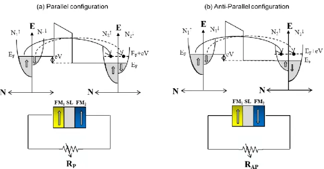
A magnetic tunnel junction (MTJ) consists of two ferromagnetic (FM) layers, called electrodes, separated by a very thin insulating layer (IL), called tunnel barrier. The thickness of the barrier ranges from a few angstroms to a few nanometers, allowing electrons to tunnel through the dielectric layer. The concept of tunnel transport or spin dependent tunnelling was introduced by Tedrow and Mersevey in 1971 [52] and four years later Julliere [53] measured the tunnel magnetoresistance (TMR) in Fe-Ge-Pb and Fe-Ge-Co structures at 4.2K. A change in the resistance of 14% as a function of the external magnetic field was found by Julliere. Julliere proposed a phenomenological model, where the spin is conserved during the tunneling process. As a consequence, the spin up(down) electrons from one electrode, FM1,
must tunnel into the up(down) states available in the other electrode, FM2, as illustrated in In
Fig. 1.2. The tunneling probability for a single electron of the first electrode is proportional to the DOS of available empty states at the second electrode. In the parallel state (Fig. 1.2a), the electrodes present the same DOS for their majority and their minority band, respectively. The
9
majority(minority) electrons of the first electrode (FM1) tunnel to the majority(minority)
electrons of the second electrode (FM2). In this configuration, the tunnel conductance, GP, is
dominated by the majority electrons. Since there is large number of states available in the majority electrons, the tunnel conductance in parallel configuration is large and thus, the resistance, RP, is low. In the antiparallel state (Fig. 1.2b), the majority(minority) band
electrons can only tunnel to the minority(majority) band electrons of the second electrode. In this case the conductance, GAP, is dominated by a mix between minority and majority band
electrons. Due to the reduced number of states available for the antiparallel configuration, the conductance is low and the resistance, RAP, is large. Hence, the tunneling conductance and
thus the resistance of MTJs depend on the relative orientation of the magnetization of the electrodes with respect to each other, as expressed as follow:
𝐺𝑃 = 𝑁1↑𝑁
2↑+ 𝑁1↓𝑁2↓ (1.5a)
𝐺𝐴𝑃 = 𝑁1↑𝑁
2↓+ 𝑁1↓𝑁2↑ (1.5b)
where 𝑁𝑖𝜎 is the density of states (DOS) at the ferromagnetic layers i for the spin direction 𝜎
at the Fermi level. The corresponding tunneling magnetoresistance ratio (TMR) is defined as: 𝑇𝑀𝑅 = 𝐺𝑃−𝐺𝐴𝑃
𝐺𝐴𝑃 =
𝑅𝐴𝑃−𝑅𝑃
𝑅𝑃 (1.6)
The relation between the TMR ratio and the spin polarization 𝑃 of both electrodes is described by the Julliere model:
𝑇𝑀𝑅 = 2𝑃1𝑃2
1−𝑃1𝑃2 (1.7)
where P1 and P2 and are the spin polarization factors (given by Eq. 1.4) for the two electrodes,
respectively. Therefore, the higher the spin polarization of the electrodes the larger the effect and if P1 = P2 = 1, the TMR ratio is infinitely high.
Fig. 1.2-Schematic representation of the tunneling process in (a) the parallel configuration and (b) the anti-parallel configuration of the two electrodes. These two band models supposes the existence of an effective barrier potential, eV. FM1, SL, FM2 correspond to first ferromagnetic layer, insulating spacer
10
In reality, the Julliere model is a simplification and the magnitude of the TMR ratio depends additionally upon the effective polarization of the electrode surfaces, the quality of the interfaces between the electrodes and the barrier, and the properties of the barrier itself. A more realistic model was proposed by Slonczewski [54], which takes into account these factors. Slonczewski expressed Eq. 1.7 by writing the transmission coefficient for each spin when taking into account the effective polarization of the DOS at each ferromagnetic/insulator interface:
𝑃𝑖 = (𝑘↑−𝑘↓)(𝜅2−𝑘↑𝑘↓)
(𝑘↑+𝑘↓)(𝜅2+𝑘↑𝑘↓) (1.8)
Where 𝑘↑ and 𝑘↓ depends on the Stoner energy, 𝜅2 = 2𝑚
𝑒(𝑈0− 𝐸𝐹)/ℏ is the effective barrier
height and 𝑈0 is the total barrier height. Using this formalism, the angular dependence of the conductance G through an insulating barrier of width 𝑑, is given by:
𝐺(𝜃) = 𝐺0[1 + 𝑃1𝑃2𝑐𝑜𝑠𝜃)] with 𝐺0 ∝ 𝑒−2𝜅𝑑 (1.9)
When 𝜅 is large, the Slonczewski model (Eq. 1.8) is equivalent to the Juliere model for infinite barrier height, 𝑈0 is large.
The improvement of deposition techniques since the first experience of Tedrow and Julliere, has allowed the fabrication of MTJ structures showing large TMR at room temperature. A reproducible large TMR (~18%) at room temperature was achieved in MTJs with an amorphous Al2O3 [55,56]. Ever since then, many researches in spin dependent
tunneling have focused on MTJs with an Al2O3as a tunnel barrier [57-59]. Although intensive
efforts in such MTJs showed that the maximum TMR only reached about 70% [60,61]. Meanwhile, extensive theoretical and experimental work has been carried out to increase the TMR by studying crystalline tunneling barriers [62,63].
Butler et al. carried out first calculations of a TMR ratio higher than 1000% in Fe(001)/ MgO/ Fe(001) crystalline junctions [62]. This enhanced TMR is due to the coherent tunneling process in MgO barrier. In Fe(001)/ MgO/ Fe(001) crystalline tunnel junctions, the electrons propagate or tunnel within specific electronic Bloch state (Δ1 for majority electrons, Δ2 and Δ5
for the minority electrons), as illustrated in Figs. 1.3a,b. Its tunneling conductance depends strongly on the symmetry of the Bloch states in the electrodes and of the evanescent states in the barrier. Thus Bloch states of different symmetry decay at different rates within the barrier. The Δ1 state decays slowest among all the states and can make a significant contribution to the
tunneling conductance.
Fig. 1.3-(a) Evolution of the density of states as a function of the numbers of MgO layers. Adapted from [62]. (b) Schematics of the electrons tunneling through (a) amorphous Al-O barrier and (b) crystalline MgO (001) barrier. Adapted from Yuasa [64]
11
The discovery of a high TMR in MTJ due to MgO produced the reorientation of research towards the improvement in the MgO deposition with a good texture with adjacent ferromagnetic layers. The most successful MTJs to date have used (001) MgO barriers with recrystallized body centered cubic (bcc) CoFeB electrodes, which have MR ratios of 200%– 600% at room temperature and over 1000% at 4.2K [65-67]. The advantage of CoFeB electrodes is that after deposition, the CoFeB/MgO/CoFeB stack is amorphous. In order to generate a lattice matching i.e crystallize the two CoFeB electrodes in the bcc MgO(001) structure, it is necessary to anneal the devices. In a MTJ device with very low resistance area (RA), studied in this thesis, the annealing is fundamental to obtain high TMR but it gives rise to several problems such as the degradation of the MgO barrier (pinholes) due to the Boron diffusion to the grain boundaries [67,68]. In order to protect the MgO barrier against Boron diffusion, the CoFeB can be replaced by CoFeB/CoFe and CoFe/CoFeB bilayers respectively, using a thin CoFe layer (≈0.5nm) at the interface to MgO. As shown in Ref. 69 this can increase the TMR from 105% to 192%.
1.1.3 Spin transfer torque (STT)
The previous section describes the TMR effect in MTJs which can be considered as a control of current flow via the magnetization state. The reverse effect, called the spin transfer torque (STT) effect, is the control of magnetization state through a spin polarized current. In other words, in a thin magnetic heterostructure device, there are two spintronics effects, MR effect and STT effect, leading to various applications, i.e. magnetic sensor in HDD read head, MRAM, STT-MRAM, STNOs, etc. Hence in order to observe the STT effect, it requires the same magnetic heterostructure as MR effect, i.e. two ferromagnetic layers FM1 and FM2,
separated by a thin spacer SL (either a metallic layer or a tunnel barrier). The physic origin (in the macrospin approach) and the effect of STT in the magnetization state of such thin magnetic heterostructure are shown in Fig. 1.4. A microscopic picture of spin transfer torque can be found in [70-72].
Consider a thin magnetic heterostructure, illustrated in Fig. 1.4a, with the magnetizations of both ferromagnetic layers, 𝑴1 and 𝑴2, are misaligned at angle θ. An electrical current passes through the structure, perpendicularly to the interfaces, with electrons flowing from the left (ferromagnetic layer FM1) to the right (ferromagnetic layer FM2).
Electrons flowing in FM1 are spin polarized along the direction of the magnetization 𝑴1 and
carry a magnetic moment 𝝁1 (𝝁1 parallel to 𝑴1), once they have passed through FM2 their
magnetic moment rotates to align with the direction of the magnetization 𝑴2. The outgoing magnetic moment is now 𝝁2.
Fig. 1.4-(a) Illustration of spin transfer torque in magnetic heterostructures, consisting of two ferromagnetic layers, FM1 and FM2, (their magnetization is aligned by an angle θ) separated with a
12
NM layer as spacer layer SL. (b) Schematic of the transferred angular momentum (𝑻 ) in the magnetization of the ferromagnetic layer FM2 which is then decomposed in two parts 𝑻1 and 𝑻2
respectively acts on the magnetization of the first ferromagnetic layer 𝑴1 and the second ferromagnetic layer 𝑴2. Adapted from [72].
The rotation of the conduction electron moments, 𝝁1 and 𝝁2, is due to a torque applied by the local magnetizations FM1 and FM2 respectively. Hence, the local magnetizations feel an equal
and opposite torque. The transverse component of the conduction electron moment 𝑻1 and 𝑻2 (see Fig. 1.4b) is transferred to the local magnetizations. This spin-transfer torque on the magnetization leads to the change in spin momentum of the localized moment per second. However the length of the magnetization vectors, 𝑴1 and 𝑴2, are conserved:
𝑑|𝑴|2
𝑑𝑡 = 2𝑴. 𝑑𝑴
𝑑𝑡 = 0 (1.10)
It results that any variation of magnetization 𝑑𝑴𝑑𝑡 is necessarily transverse to the magnetization. The total transferred angular momentum 𝑻 in the system is a sum of two moments 𝑻1 and 𝑻2, where 𝑻1 is a torque transferred to 𝑴1 and 𝑻2 is a torque transferred to 𝑴2. In practice, the
magnetization of FM1 is designed to be fixed (polarizing layer PL) for example by using a
Synthetic Anti-Ferromagnetic (SAF) structure [73-75] or a thick electrode FM1, in order to
make FM1 less susceptible to spin torque and mainly serves as a polarizer to provide spin
polarization. Whereas, the magnetization of FM2 is usually thin and can be excited by spin
torque, called as free layer FL. In this case, the spin torque acting on the free-layer magnetization 𝒎due to the misalignment with the polarizing layer magnetization 𝒑 is given by two terms. The first term, called the ‘spin transfer torque STT term 𝑻∥’, corresponds to a
transfer of the transverse component of the spin momentum that lies in the plane of 𝒎 and 𝒑, while the second term, called field-like term 𝑻⊥, corresponds to a transfer of the transverse
component that is perpendicular to the plane of 𝒎 and 𝒑. The spin torque 𝑻𝑠 including two terms is described as follow:
𝑻𝑠 = 𝑻∥+ 𝑻⊥= 𝛾0𝑎𝑗𝒎× (𝒎× 𝒑) + 𝛾0𝑏𝑗(𝒎× 𝒑) (1.11)
Here, 𝒎 is the unitary magnetization vector of the free layer given by 𝒎 =𝑀𝑴
𝑠 with Ms is the spontaneous magnetization. 𝛾0 is the gyromagnetic factor, 𝑎𝑗 is the spin torque amplitude proportional to the applied current, and 𝑏𝑗 is the prefactor of the field-like term depending on
the net current charge. In this thesis, the contribution from 𝑏𝑗 will be neglected, as it is
assumed that 𝑏𝑗 does not have strong impact on the dynamics of MTJ-based STNOs, 𝑎𝑏𝑗
𝑗 ≪ 1. This assumption is justified by the maximal value encountered in MTJ for 𝑏𝑗, which is 30%
13
1.2 Magnetization Dynamics
It has been introduced the physic origin of spin transfer torque STT in thin magnetic heterostructures. In this section the effect of STT on magnetization dynamics of STNOs in the macrospin approximation will be discussed. This Section starts with the introduction of Landau-Lifsthitz-Gilbert-Slonczewski (LLGS) equation. The constant energy trajectory obtained by solving the LLGS equation will be discussed. The evolution of magnetization dynamics under external control parameters, applied field and applied current density, will be shown for the case of zero temperature and finite temperature.
1.2.1 Introduction to LLGS equation
The magnetization dynamics is described by the Landau-Lifshitz-Gilbert equation, that includes the conservative precession of the magnetization and the damping torques (first two terms of eq. 1.12). In order to take the effect of spin transfer into account, the longitudinal spin torque 𝑻∥ is included to the LLG equation (third term of eq. 1.12), thus leading to the Landau-Lifsthitz-Gilbert-Slonczewski (LLGS) equation as given by eq. 1.12, i.e. The bj term
is neglected, two magnetization dynamical modes occur under the influence of STT in its simplest form (aj ∝ Japp).
𝑑𝒎
𝑑𝑡 = −𝛾0(𝒎 × 𝑯𝒆𝒇𝒇) + 𝛼 (𝒎 × 𝑑𝒎
𝑑𝑡) − 𝛾0𝑎𝑗𝒎 × (𝒎 × 𝒑) (1.12)
Here 𝛾0is the gyromagnetic factor given by 𝛾0 = 𝜇0𝛾 = 2.21𝑥105 𝐴𝑠𝑚 with 𝜇0 is vacuum permeability.𝛼 is the natural damping constant, 𝑀𝑠 is the saturation magnetization and 𝑎𝑗 is the spin torque amplitude proportional to the applied current density 𝐽𝑎𝑝𝑝 given by the general
expression: 𝑎𝑗 =2𝑒ℏ 𝜇𝐽𝑎𝑝𝑝
0𝑀𝑠𝑡𝜂 (1.13)
Where, t is the thickness of the STNO device and 𝜂 is the spin polarization value.
𝑯𝒆𝒇𝒇 is the effective field given by the negative gradient of the free energy density E with respect to the unitary magnetization vector 𝒎, 𝑯𝒆𝒇𝒇 = −𝜇 1
0𝑀𝑠𝑉
𝛿𝐸
𝛿𝒎. It is important to note
that the free energy density E is the sum of all potential energies Ei resulting from any fields
𝑯i acting on 𝒎. For STNO devices the most important energy E terms are (i) the Zeeman
energy, 𝐸𝑎𝑝𝑝 = −𝜇0𝑀𝑠𝑉𝒎𝑯𝒂𝒑𝒑, due to an external applied bias field 𝑯𝒂𝒑𝒑, (ii) the demagnetization energy due to geometry of the sample, 𝐸𝑑, (iii) the anisotropy energy due to
crystalline or interfacial energies 𝐸𝑢, and (iv) the exchange energy due to spin-dependent
quantum mechanical interactions 𝐸𝑒𝑥. Detail of each contribution fields can be found for instance in [71]. In the case of single domain or macrospin model, the exchange interaction is assumed to be sufficiently strong so that all of the magnetic moments in a device layer are aligned and move together. In this model the magnitude of the moment is constant in time. Since the exchange energy is negligible 𝑯𝒆𝒙 = 0, the effective field can be described as follow:
14
Due to the demagnetization and anisotropy contributions to the effective field 𝑯𝒆𝒇𝒇, the equilibrium orientation of the magnetization 𝒎 will be different from the direction of the applied field 𝑯𝒂𝒑𝒑.
A simple illustration of the evolution of the magnetization dynamic under the LLGS equation is given in Fig. 1.5. The magnetization dynamic under the torque 𝑻 exerted by a magnetic field 𝑯𝒆𝒇𝒇 is given by the first term in the right-hand side of eq. 1.12 (conservative term). The term says simply that the magnetization 𝒎 precesses around the effective magnetic field 𝑯𝒆𝒇𝒇 at a constant energy trajectory (constant magnitude), i.e. closed loop trajectory, as
illustrated in Fig. 1.5a (red curve). The second term is a relaxation term and describes the energy losses (energy dissipation) due to interaction of the magnetization with its environment. The parameter that characterizes the losses is the Gilbert damping constant α. It should be noted that α is rather small, α ~ 0.01 in typical magnetic materials used for spin torque experiments. The damping torque itself is, usually, comparable in magnitude with the spin transfer torque and much smaller than the conservative precessional torque −𝛾0[𝒎 ×
𝑯𝒆𝒇𝒇]. Hence, the damping term can be considered as a small perturbation to the precessional
term.From any initial position, the damping torque will relax the magnetization towards its energy minimum (low energy state), i.e. realigned with the local effective field, on a timescale given by Ms (few nanoseconds). The effect of damping on the overall trajectory is shown in
Fig. 1.5b. As the magnetic moment relaxes, it will sample a family of nearly constant energy orbits. To first approximation, these are the orbits that are stabilized by the transfer of spin, STT, from the applied current. This STT, i.e. described by the last term of eq. 1.12, can be either as an energy source or an additional dissipative (or damping) contribution for the system, depending on the current sign. In the case of an energy source or gain, the STT cancels and compensates the damping torque and thus brings the magnetization into the steady state precession (closed loop trajectory), as illustrated in Fig. 1.5c. In contrast to this, in the case of an additional dissipation, the STT enhances the damping torque and relaxes the magnetization towards the energy minimum.
Fig. 1.5-Illustration of the evolution of the magnetization dynamic (red curve): (a) conservative precession term (b) negative damping (dissipative term) (c) STT term, i.e. STT cancels the negative damping torque. Adapted from [76].
The illustration above is a very general picture of magnetization dynamic in the presence and the absence of damping term and spin transfer torque term. In the next Subsection, the solution of LLGS equation within the macrosin approach will be discussed in order to get a more intuitive macrospin description of the magnetization dynamic for magnetic thin film geometry, by considering special trajectories and their frequencies. Here the simplest magnetic thin film geometry, i.e. an in-plane magnetized MTJ configuration, where the free layer and polarizing layer are in-plane magnetized, is considered which corresponds to the devices studied in this thesis (Fig. 1.6). In coordinate system, the free magnetic layer lies in the x-y plane, axis z is normal to the thin film plane, and the easy axis of the in-plane
15
anisotropy is along the x axis. The in plane rotation is characterized by the spherical angle 𝜑 and the out plane rotation is characterized by the spherical angle 𝜃.
Fig. 1.6-Left: definition of the (x, y, z) coordinate system and the spherical angles 𝜑, 𝜃. Right: the free layer considered is an in-plane magnetized thin film.
A uniaxial magnetocrystalline (MCA) anisotropy field 𝑯𝒖 along x-axis direction is
considered of amplitude Ku (Ku>0), 𝑯𝒖 =𝜇2𝐾𝑢
0𝑀𝑠(𝑚𝑥 0 0). The demagnetizing effect are included by the demagnetizing tensor 𝑵⃡ = (𝑁𝑋,𝑁𝑌, 𝑁𝑍). For a nanopillar geometry, 𝑯𝒅 is assumed in the z-axis direction, 𝑯𝒅 = −𝑀𝑠(0 0 𝑁𝑍𝑚𝑍). The external applied field, 𝑯𝒂𝒑𝒑,
is applied parallel to the easy axis of the in-plane anisotropy (in the x-direction) so that 𝑯𝒂𝒑𝒑 = (𝐻𝑎𝑝𝑝,𝑥 0 0). The magnetic energy density E of this system can be written as the
sum of the anisotropy, demagnetizating (magneto-dipolar), and applied field energies:
𝐸 = 𝐾𝑢[1 − 𝑚𝑥2]𝑉 +12𝜇0𝑀𝑠2(𝑁𝑧𝑚𝑧2)𝑉 + −𝜇0𝑀𝑠𝐻𝑎𝑝𝑝𝑚𝑥𝑉 (1.15)
With (𝑚𝑥, 𝑚𝑦, 𝑚𝑧) = (𝑐𝑜𝑠𝜃𝑐𝑜𝑠𝜑, 𝑐𝑜𝑠𝜃𝑠𝑖𝑛𝜑, 𝑠𝑖𝑛𝜃) 1.2.2 Constant energy trajectories
Since the damping torque and the spin torque are small as compared to the precession (conservative) torque, a first approximation to the magnetization precession trajectories at constant energy trajectories (eigenmodes of the undamped system) can be made. In a macrospin description, the constant energy trajectories of the magnetization dynamics are determined by the conservative precession term (first term) of LLGS eq. 1.12, (i.e. for α=0 and 𝑎𝑗=0). The solution of the precession term for a given initial energy density E0 (eq. 1.15)
yields the static and periodic solutions which are shown in Fig. 1.7. There are three static states, see Figs. 1.7a,b, (defined by 𝜕𝒎𝜕𝑡 = 0) which are the in-plane energy minimum (along the in-plane easy axis), the out of-plane energy maximum (representing the demagnetization energy cost when rotating M perpendicular to the film plane) and the saddle point (in-plane hard axis). Preparing the system initially in one of these three static states, the system does not change and remain in its initial state (constant energy). When perturbing the system, the magnetization will follow period orbits around either the energy minimum or the energy maximum as indicated by the colored lines in Figs. 1.7a,b. The precession around the energy minimum (mx=1) is generally called in-plane precession (IPP) since the energy minimum of
a thin magnetic film is in-plane (Fig. 1.7a) and the precession around the out-of-plane energy maximum is called out-of-plane precession (OPP) (Fig. 1.7b) [70-72,77]. The IPP magnetization trajectories are described by a windscreen wiper motion in a counter-clockwise oscillation sense. The in-plane excursion angle of IPP mode trajectories increase with
16
increasing initial energy Eo. When the trajectories pass through the energy saddle points
(in-plane hard axis), the trajectories bifurcate into two energetically equivalent OPP modes (one for positive mz and one for negative mz). These OPP modes trajectories are described by a
circular motion, or a tilted circular motion in a clockwise rotation sense around the energy maximum.
Due to the non-linearity of the equation of motion, 𝑯𝒆𝒇𝒇 (𝒎 ), there is a strong
dependence of the precession frequency on the precession amplitude, which is different for the IPP and OPP mode, as given in Fig. 1.7c. They are plotted as a function of the initial energy Eo, expressed by the maximum 𝑚𝑧+ value on the trajectory. For IPP mode, the
frequency decreases with increasing amplitude of initial energy (redshift) since the length of the orbit increases faster than the local velocity. Close to the saddle point, the local velocity goes to zero, explaining the zero frequency at the transition from IPP to OPP. For the OPP mode the frequency increases with increasing amplitude (blueshift). The frequency value is given by the out-of-plane demagnetization field which is proportional to the out-of-plane magnetization component mz.
Fig. 1.7-(a) Conservative IPP and (b) OPP oscillations as a function of the initial energy Eo. (c)
Precession frequency for conservative IPP and OPP oscillations as a function of the initial energy Eo,
expressed by the maximum 𝑚𝑧+ value on the trajectory. Adapted from [72].
Adding damping in the system, the magnetization dynamics are determined by the conservative precession term (first term) and the damping term (second term) of LLGS eq. 1.12, (i.e. for α=0.01-0.02 depending of the materials and 𝑎𝑗=0). The precession term will
change the stability of the three static solutions. Now, only the energy minimum is stable, leading to IPP oscillations at small precession angles around the energy minimum. This means that the energy maximum and saddle point are not stable against small perturbations (the damping term can be considered as a small perturbation to the precessional term), which will relax the magnetization on a spiral orbit away from the energy maximum or the saddle point towards the stable energy minimum. These small IPP precession angles correspond to the FMR excitations and are indicated for comparison in Fig. 1.7a.
Including the STT in the system, i.e. full LLGS equation, their contribution can be either, an energy source for the system if the spin-torque opposes the damping torque, or an additional dissipation (or damping) contribution if the spin-torque torque has the same direction as the damping torque. In the case of an additional dissipation, the motion is damped and thus the static state in the energy minimum is stable, i.e. in the in-plane magnetized MTJ configuration, the spin polarization 𝒑 is collinear to the effective field 𝑯𝒆𝒇𝒇 of the free layer energy minimum.In contrast to this, for the case of an energy source, the motion is excited away from the static state and thus the static state is unstable. Upon increasing the current density from zero, an initially stable state can become unstable. The current value for which
17
this occurs is called the critical current Jth.When the initial static state become unstable, the
magnetization can either transit into another static state or into a dynamic state, depending on the current amplitude. It is important to note that the STT does not change the energy surface, the STT moves the magnetization along the energy surface until the magnetization stabilizes on a periodic orbit defined by the precession term (see Figs. 1.7a,b). For further understanding on the transition from the static state to a dynamic state, the illustration of the general features of the dynamic state for the case of in-plane magnetized magnetic thin film will be discussed in the following.
1.2.3 State diagram of an in plane magnetoresistive device (0K)
State diagram defines the different static and dynamic states in the current-field plane. As already mentioned, for in plane magnetoresistive devices, the spin torque is more or less collinear with the damping torque and the free layer has a uniaxial anisotropy (given by an anisotropy field 𝑯𝒖) in the same direction as the applied field, 𝑯𝒂𝒑𝒑. For this configuration the state diagram has been predicted from macrospin simulations at T=0K as shown in Fig. 1.8. This diagram is asymmetric as a function of the sign of current Japp (normalized) and
field, 𝑯𝒂𝒑𝒑, which is normalized by anisotropy field 𝑯𝒖. At zero applied field and no current, there are two energy minima (stable states) which are given by the parallel (P) and antiparallel (AP) alignment of the free layer magnetization with respect to the polarizer magnetization direction. The initial state defines the evolution of the magnetization with applied current. This magnetization dynamic evolution is summarized as follows:
(i) In the sub-critical regime (Japp<Jth1) the spin torque acts such that for one sign of the
current, it enhances the natural damping and stabilizes the initial state, while for the opposite current direction it will counteract damping and destabilize the initial state.
(ii) Above the critical regime (Japp >Jth1), for the correct sign, the magnetization goes into
steady state oscillations of the type IPP, which are around the initial stable state (energy minimum).
Fig. 1.8-Left: State diagram of the magnetization state in In-plane magnetized structures. Right, IPP and OPP trajectories in the energy landscape as a function of in-plane angle 𝜑. Adapted from [72].
(iii) Upon increasing the current further, the oscillation amplitude increases and the magnetization transits into steady state OPP oscillations when the current is larger than a second threshold current (Jth1> Japp >Jth2). This transition occurs however only when the bias
field is larger than the anisotropy field (Happ>Hu). For Happ<Hu, the magnetization transits
from the IPP steady state oscillations into the reversed static state. This transition into the OPP state or the reverse static state occurs, when the IPP trajectories are pushed up on the energy landscape such that they pass through the energy saddle point.