Publisher’s version / Version de l'éditeur:
Optics Express, 25, 11, pp. 12222-12236, 2017-05-29
READ THESE TERMS AND CONDITIONS CAREFULLY BEFORE USING THIS WEBSITE. https://nrc-publications.canada.ca/eng/copyright
Vous avez des questions? Nous pouvons vous aider. Pour communiquer directement avec un auteur, consultez la
première page de la revue dans laquelle son article a été publié afin de trouver ses coordonnées. Si vous n’arrivez pas à les repérer, communiquez avec nous à [email protected].
Questions? Contact the NRC Publications Archive team at
[email protected]. If you wish to email the authors directly, please see the first page of the publication for their contact information.
This publication could be one of several versions: author’s original, accepted manuscript or the publisher’s version. / La version de cette publication peut être l’une des suivantes : la version prépublication de l’auteur, la version acceptée du manuscrit ou la version de l’éditeur.
For the publisher’s version, please access the DOI link below./ Pour consulter la version de l’éditeur, utilisez le lien DOI ci-dessous.
https://doi.org/10.1364/OE.25.012222
Access and use of this website and the material on it are subject to the Terms and Conditions set forth at
Disorder effects in subwavelength grating metamaterial waveguides
Ortega-Moñux, Alejandro; Čtyroký, Jiří; Cheben, Pavel; Schmid, Jens H.;
Wang, Shurui; Molina-Fernández, Íñigo; Halir, Robert
https://publications-cnrc.canada.ca/fra/droits
L’accès à ce site Web et l’utilisation de son contenu sont assujettis aux conditions présentées dans le site LISEZ CES CONDITIONS ATTENTIVEMENT AVANT D’UTILISER CE SITE WEB.
NRC Publications Record / Notice d'Archives des publications de CNRC:
https://nrc-publications.canada.ca/eng/view/object/?id=b4c49737-9400-445d-bebc-e07acf4f2635 https://publications-cnrc.canada.ca/fra/voir/objet/?id=b4c49737-9400-445d-bebc-e07acf4f2635Disorder effects in subwavelength grating
metamaterial waveguides
A
LEJANDROO
RTEGA-M
OÑUX,
1,*J
IŘÍČ
TYROKÝ,
2P
AVELC
HEBEN,
3J
ENSH. S
CHMID,
3S
HURUIW
ANG,
3Í
ÑIGOM
OLINA-F
ERNÁNDEZ,
1ANDR
OBERTH
ALIR11
Dpto. de Ingeniería Comunicaciones, ETSI Telecomunicación, Universidad de Málaga, 29010 Málaga, Spain
2
Institute of Photonics and Electronics, CAS, Chaberská 57, 182 51 Prague, Czech Republic
3
National Research Council Canada, 1200 Montreal Road, Ottawa, Ontario K1A0R6, Canada
Abstract: Subwavelength grating (SWG) waveguides are integrated photonic structures with
a pitch substantially smaller than wavelength for which they are designed, so that diffraction effects are suppressed. SWG operates as an artificial metamaterial with an equivalent refractive index which depends on the geometry of the structure and the polarization of the propagating wave. SWG waveguides have been advantageously used in silicon photonics, resulting in significant performance improvements for many practical devices, including highly efficient fiber-chip couplers, waveguide crossings, broadband multimode interference (MMI) couplers, evanescent field sensors and polarization beam splitters, to name a few. Here we present a theoretical and experimental study of the influence of disorder effects in SWG waveguides. We demonstrate via electromagnetic simulations and experimental measurements that even a comparatively small jitter (~5 nm) in the position and size of the SWG segments may cause a dramatic reduction in the transmittance for wide (multimode) SWG waveguides, while for narrow (single mode) waveguides this effect is negligible. Our study shows that the impact of the jitter on SWG waveguide performance is directly related to the modal confinement.
© 2017 Optical Society of America
OCIS codes: (130.0130) Integrated optics; (250.5300) Photonic integrated circuits; (130.3120) Integrated optics devices; (050.6624) Subwavelength structures; (160.3918) Metamaterials.
References and links
1. S. M. Rytov, “The electromagnetic properties of finely layered medium,” Sov. Phys. JETP 2, 466–475 (1956). 2. M. W. Farn, “Binary gratings with increased efficiency,” Appl. Opt. 31(22), 4453–4458 (1992).
3. P. Cheben, D.-X. Xu, S. Janz, and A. Densmore, “Subwavelength waveguide grating for mode conversion and light coupling in integrated optics,” Opt. Express 14(11), 4695–4702 (2006).
4. P. Cheben, P. J. Bock, J. H. Schmid, J. Lapointe, S. Janz, D. X. Xu, A. Densmore, A. Delâge, B. Lamontagne, and T. J. Hall, “Refractive index engineering with subwavelength gratings for efficient microphotonic couplers and planar waveguide multiplexers,” Opt. Lett. 35(15), 2526–2528 (2010).
5. P. Cheben, J. H. Schmid, S. Wang, D.-X. Xu, M. Vachon, S. Janz, J. Lapointe, Y. Painchaud, and M.-J. Picard, “Broadband polarization independent nanophotonic coupler for silicon waveguides with ultra-high efficiency,” Opt. Express 23(17), 22553–22563 (2015).
6. D. Benedikovic, P. Cheben, J. H. Schmid, D. X. Xu, B. Lamontagne, S. Wang, J. Lapointe, R. Halir, A. Ortega-Moñux, S. Janz, and M. Dado, “Subwavelength index engineered surface grating coupler with sub-decibel efficiency for 220-nm silicon-on-insulator waveguides,” Opt. Express 23(17), 22628–22635 (2015).
7. D. Benedikovic, C. Alonso-Ramos, P. Cheben, J. H. Schmid, S. Wang, R. Halir, A. Ortega-Moñux, D. X. Xu, L. Vivien, J. Lapointe, S. Janz, and M. Dado, “Single-etch subwavelength engineered fiber-chip grating couplers for 1.3 µm datacom wavelength band,” Opt. Express 24(12), 12893–12904 (2016).
8. X. Xu, H. Subbaraman, J. Covey, D. Kwong, A. Hosseini, and R. T. Chen, “Complementary metal–oxide– semiconductor compatible high efficiency subwavelength grating couplers for silicon integrated photonics,” Appl. Phys. Lett. 101(3), 031109 (2012).
9. A. Sánchez-Postigo, J. Gonzalo Wangüemert-Pérez, J. M. Luque-González, Í. Molina-Fernández, P. Cheben, C. A. Alonso-Ramos, R. Halir, J. H. Schmid, and A. Ortega-Moñux, “Broadband fiber-chip zero-order surface grating coupler with 0.4 dB efficiency,” Opt. Lett. 41(13), 3013–3016 (2016).
10. J. Gonzalo Wangüemert-Pérez, P. Cheben, A. Ortega-Moñux, C. Alonso-Ramos, D. Pérez-Galacho, R. Halir, I. Molina-Fernández, D. X. Xu, and J. H. Schmid, “Evanescent field waveguide sensing with subwavelength grating structures in silicon-on-insulator,” Opt. Lett. 39(15), 4442–4445 (2014).
11. J. Flueckiger, S. Schmidt, V. Donzella, A. Sherwali, D. M. Ratner, L. Chrostowski, and K. C. Cheung, “Sub-wavelength grating for enhanced ring resonator biosensor,” Opt. Express 24(14), 15672–15686 (2016). 12. H. Yun, Y. Wang, F. Zhang, Z. Lu, S. Lin, L. Chrostowski, and N. A. Jaeger, “Broadband 2 × 2 adiabatic 3 dB
coupler using silicon-on-insulator sub-wavelength grating waveguides,” Opt. Lett. 41(13), 3041–3044 (2016). 13. R. Halir, P. Cheben, J. M. Luque-González, J. D. Sarmiento-Merenguel, J. H. Schmid, J. G. Wangüemert-Pérez,
D. X. Xu, S. Wang, A. Ortega-Moñux, and I. Molina-Fernández, “Ultra-broadband nanophotonic beamsplitter using an anisotropic sub-wavelength metamaterial,” Laser Photonics Rev. 10(6), 1039–1046 (2016).
14. Y. Xiong, J. G. Wangüemert-Pérez, D.-X. Xu, J. H. Schmid, P. Cheben, and W. N. Ye, “Polarization splitter and rotator with subwavelength grating for enhanced fabrication tolerance,” Opt. Lett. 39(24), 6931–6934 (2014). 15. L. Liu, Q. Deng, and Z. Zhou, “Manipulation of beat length and wavelength dependence of a polarization beam
splitter using a subwavelength grating,” Opt. Lett. 41(21), 5126–5129 (2016).
16. Y. Xu and J. Xiao, “Ultracompact and high efficient silicon-based polarization splitter-rotator using a partially-etched subwavelength grating coupler,” Sci. Rep. 6(1), 27949 (2016).
17. D. Pérez-Galacho, D. Marris-Morini, A. Ortega-Moñux, J. G. Wangüemert-Pérez, and L. Vivien, “Add/Drop Mode-Division Multiplexer Based on a Mach–Zehnder Interferometer and Periodic Waveguides,” IEEE Photonics J. 7(4), 7800907 (2015).
18. J. Wang, R. Ashrafi, R. Adams, I. Glesk, I. Gasulla, J. Capmany, and L. R. Chen, “Subwavelength grating enabled on-chip ultra-compact optical true time delay line,” Sci. Rep. 6(1), 30235 (2016).
19. P. J. Bock, P. Cheben, A. V. Velasco, J. H. Schmid, A. Delâge, M. Florjańczyk, J. Lapointe, D.-X. Xu, M. Vachon, S. Janz, and M. L. Calvo, “Subwavelength grating Fourier-transform interferometer array in silicon-on-insulator,” Laser Photonics Rev. 7(6), 67–70 (2013).
20. J. S. Penades, A. Ortega-Moñux, M. Nedeljkovic, J. G. Wangüemert-Pérez, R. Halir, A. Z. Khokhar, C. Alonso-Ramos, Z. Qu, I. Molina-Fernández, P. Cheben, and G. Z. Mashanovich, “Suspended silicon mid-infrared waveguide devices with subwavelength grating metamaterial cladding,” Opt. Express 24(20), 22908–22916 (2016).
21. R. Halir, P. J. Bock, P. Cheben, A. Ortega-Moñux, C. Alonso-Ramos, J. H. Schmid, J. Lapointe, D. Xu, J. G. Wangüemert-Pérez, I. Molina-Fernández, and S. Janz, “Waveguide sub-wavelength structures: a review of principles and applications,” Laser Photonics Rev. 9(1), 25–49 (2015).
22. L. R. Chen, “Subwavelength grating waveguide devices in silicon-on-insulators for integrated microwave photonics (Invited Paper),” Chin. Opt. Lett. 15, 010004 (2017).
23. D. Melati, A. Melloni, and F. Morichetti, “Real photonic waveguides: guiding light through imperfections,” Adv. Opt. Photonics 6(2), 156–224 (2014).
24. D. Pérez-Galacho, R. Halir, L. F. Zavargo-Peche, J. G. Wangüemert-Pérez, A. Ortega-Moñux, I. Molina-Fernández, and P. Cheben, “Adiabatic transitions for sub-wavelength grating waveguides,” Proceedings of the European Conference on Integrated Optics, Barcelona, Spain, 18–20 April 2012, paper 71.
25. J. D. Sarmiento-Merenguel, A. Ortega-Moñux, J. M. Fédéli, J. G. Wangüemert-Pérez, C. Alonso-Ramos, E. Durán-Valdeiglesias, P. Cheben, Í. Molina-Fernández, and R. Halir, “Controlling leakage losses in subwavelength grating silicon metamaterial waveguides,” Opt. Lett. 41(15), 3443–3446 (2016). 26. L. Zavargo-Peche, A. Ortega-Moñux, J. G. Wangüemert-Pérez, and I. Molina-Fernández, “Fourier based
combined techniques to design novel sub-wavelength optical integrated devices,” Prog. Electromagnetics Res. 123, 447–465 (2012).
27. J. Čtyroký, “3-D bidirectional propagation algorithm based on Fourier series,” J. Lightwave Technol. 30(23), 3699–3708 (2012).
28. T. Barwicz and H. Smith, “Evolution of line-edge roughness during fabrication of high-index-contrast microphotonic devices,” J. Vac. Sci. Technol. B 21(6), 2892–2896 (2003).
29. C. L. Chen, Foundations for guide-wave optics, (Wiley-interscience, Hoboken, New Jersey, 2007). 1. Introduction
An optical waveguide core comprising a grating with a period (pitch) smaller than one half of the wavelength for which it is designed to operate, behaves as an artificial metamaterial with an equivalent refractive index which depends on the geometry of the structure and the polarization of the incident wave [1–3]. Since the first experimental demonstration of an optical waveguide with a subwavelength periodic core [4], these structures, also called subwavelength gratings (SWGs), have found many applications in integrated optics, for example as highly efficient fiber-chip couplers [3–9], low-loss waveguide crossings, evanescent field sensors [10,11], broadband directional couplers [12] and multimode interference (MMI) [13] couplers, polarization beam splitters [14–16], wavelength division [4] and mode division [17] multiplexers, delay lines [18], Fourier-transform spectrometers [19] and suspended (membrane) waveguides for mid-infrared applications [20]. Exhaustive
reviews of SWG fundamentals and applications can be found in [21, 22]. SWG waveguide devices are typically fabricated on the silicon-on-insulator (SOI) platform, where the main materials are silicon (nSi ~3.47, waveguide core) and silicon dioxide (nSiO2 ~1.44, cladding).
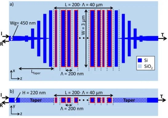
The SWG waveguides often comprise a z-periodic segmented core, as first demonstrated in [4]. The structure is schematically shown in Fig. 1(a). The grating pitch is sufficiently small to support the propagation of guided waves while diffraction and Bragg effects are suppressed. A judicious design of the geometrical parameters of the SWG core, i.e. width (W), pitch (Λ), and duty cycle (lSi/Λ) allows engineering of the waveguide properties,
including the mode field confinement, the effective index and the dispersion.
Fig. 1. (a) Geometry of an ideal z-periodic subwavelength grating waveguide (light propagates along the z direction), as first demonstrated in ref [4]. (b) A subwavelength grating waveguide with random variations (jitter) in the positions and dimensions of the silicon segments due to fabrication imperfections.
In this work, we report a detailed study of the effects of fluctuations in waveguide geometry [see Fig. 1(b)], also called jitter, inherent to any fabrication process, on the performance of SWG waveguide structures. While the effects of fabrication imperfections in conventional channel waveguides and photonic crystal slab waveguides have been extensively studied in the past (see e.g [23]. for a comprehensive review on this topic), the effect of the jitter on the performance of periodic SWG waveguides has not yet been reported. In agreement with previous experimental results demonstrating high performance single mode SWG structures, we find that the effect of a moderate jitter on narrow waveguides (single mode, W ∼0.5 µm) can be negligible. However, we show that for wider waveguides (multimode, W > 1 µm) even a small jitter can produce strong random variations in waveguide transmittance, substantially degrading device performance. Specifically, by using electromagnetic simulations and experimental measurements, we find that a jitter as small as 5 nm (2.5% of a typical SWG pitch Λ = 200 nm) in a 3 µm wide SWG waveguide can induce a propagation loss penalty of ∼3 dB per 100 µm as well as significant back-reflections. It is found that both propagation loss and reflectance vary strongly with wavelength and the specific geometry of the jitter.
This paper is organized as follows. In the next section we define the test structures and parameters which will be used to analyze the effects of the jitter. In sections 3 and 4 we report on simulation studies and experimental measurements, and evaluate the statistical significance of the results. In section 5, we outline an intuitive explanation of the underlying physical phenomena and their implications for jitter influence in different waveguide geometries. Finally, the conclusions are drawn.
2. Definitions of the test structures and parameters
Figure 2 shows the schematics of the basic test structure used throughout in this work. The structure comprises a wide SWG waveguide and two adiabatic tapers to convert the mode of the interconnecting Si-wire waveguide to the SWG waveguide mode [24]. The nominal width of the SWG waveguide (W = 3 µm) is chosen large enough to assure a strong lateral confinement of the fundamental Floquet-Bloch mode. The grating pitch Λ = 200 nm was selected safely below the Bragg period (ΛB ~280 nm at = 1.47 µm), to minimize losses due
length of L = 200·Λ = 40 µm. The nominal duty cycle was chosen as DC = lSi / Λ = 50%, as it
provides sufficient vertical confinement to mitigate power leakage to the silicon substrate [25]. Another important consideration when choosing this initial set of geometrical parameters was our interest in the jitter influence on a realistic structure related to a practical application, namely an ultra-broadband 2 × 2 MMI coupler, which we recently reported using the same technological platform [13].
Fig. 2. Schematics of the nominal test structure. Light from an input silicon wire waveguide is coupled via an adiabatic taper into a wide SWG waveguide with a specifically engineered jitter distribution, and subsequently coupled via the second adiabatic taper to a silicon wire output waveguide. Segments with red contours represent jittered silicon strips. I, T and R denote the input, the transmitted and the reflected light, respectively. (a) Top view and (b) side view. Dimensions are not to scale.
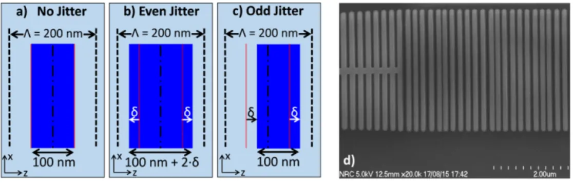
In the following we will focus on jitter in the longitudinal (z-constant) interfaces of the silicon segments. The effect of the jitter in the lateral interfaces can be considered negligible compared to the longitudinal jitter, because of the large mode size in lateral direction, hence a substantially reduced mode overlap with the lateral interfaces. The nominal period of the structure is shown in Fig. 3(a), with a silicon stripe nominal length lSi = 100 nm placed at the
center of the grating period of Λ = 200 nm. For a displacement δ of both longitudinal interfaces in opposite directions, which we refer to as even jitter, the structure remains symmetric within the period while the duty cycle changes, as illustrated in Fig. 3(b). On the other hand, for a displacement of both interfaces in the same direction [Fig. 3(c)], which we refer to as odd jitter, the duty cycle remains constant, but the structure is no longer symmetric within the period. These two respective jitter definitions are chosen with a practical consideration in mind: an ideal z-periodic waveguide can be represented as a concatenation of symmetric periods with a specific duty cycle, so the natural way of studying the effect of fabrication imperfections is to analyze the influence of fluctuations in the waveguide symmetry (odd jitter) and the duty cycle (even jitter).
To design the test structures we first generate a vector of displacements δ, which is a sequence of 200 random numbers (one for each period of the test structure) following a normal distribution with zero mean and standard deviation (jitter strength) σ. Then we obtain
a specific realization, which is a test structure built from the generated jitter sequence δ where one of the two types of jitters (even or odd) is applied. In the case of even jitter, the i-th element of δ is subtracted from the start position of the i-th segment and added to the end position of the i-th segment [Fig. 3(b)]; in the case of odd jitter, the i-th element of δ is added to both the start and end position of the i-th segment [Fig. 3(c)]. Note that two test structures with the same jitter strength (σ) and the same type of jitter (even or odd), but defined from two different jitter sequences δ1 and δ2, are actually two different realizations of the same experiment. Figure 3(d) shows a scanning electron microscope (SEM) image of one of the fabricated test structures, which was defined using odd jitter with σ = 20 nm. The periodicity fluctuations in this jittered SWG waveguide can be clearly observed.
Fig. 3. (a)-(c) Jitter geometrical definition. (a) No jitter. The nominal period is symmetric with a duty cycle DC = 50%. (b) Even jitter. The period remains symmetric but the duty cycle fluctuates around 50%. For δ > 0 the Si stripe is longer than nominal, i.e. DC > 50%. (c) Odd jitter. The DC remains constant (50%) but the period is no longer symmetric. For δ > 0 the Si stripe shifts to the right. (d) Scanning electron microscope (SEM) image of a fabricated SWG waveguide structure (top view). The image shows the end of the wire-to-SWG taper (left) and the first 22 periods of the SWG waveguide, where the effect of the jitter (σ = 20 nm, intentionally generated) is clearly visible.
A comprehensive set of experiments was carried out to ensure the statistical significance of the results. We focused on the analysis of the power transmittance (T), the reflectance (R) and the radiation losses (L = 1 – T – R) for different realizations of the test structure, using the jitter type (even or odd) and strength (σ) as parameters, for a wavelength range 1470 nm – 1580 nm. In Table 1, we summarize the different jitter realizations used in this work, for both the simulations and experimental studies.
Table 1. Summary of specific jitter realizations utilized in the simulations and experimental studies
R
N N
λ σ (nm) Jitter type
Section 3: Simulation results
2D 11 111 2, 5, 10, 20 Odd 2D 200 1 0, 2, 5, 10, 20 Odd & Even 3D 1 61 0, 2, 5, 10, 20 Odd & Even Section 4: Experimental results 4-11 11001
0, 2, 5, 10, 20 Odd 0, 1, 2.5, 5,
10
Even
R
N is the number of different realizations for each jitter strength (σ) and type. Nλ
is the number of points in the wavelength sweep for each jitter strength (σ) and type. 3. Simulation results
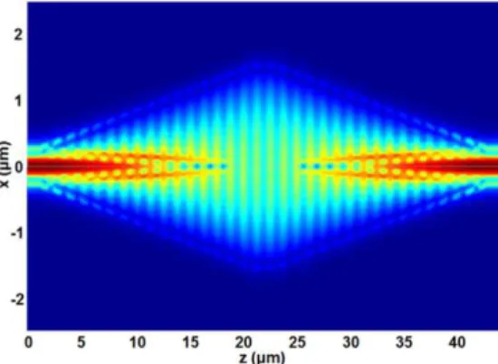
While most of the simulations were carried out using our 2D simulation tool based on the Fourier Eigenmode Expansion Method (F-EEM) [26], the accuracy of these results was examined using rigorous 3D full-vectorial simulations [27]. We have also employed the 3D simulation tool to design the adiabatic tapers that connect the Si-wire to the SWG waveguide
at both sides of the test structure. Figure 4 shows the xz cut of the electric field distribution propagating through two of these tapers arranged in a back-to-back configuration (Ltaper = 20
m). The calculated insertion losses are well below 0.1dB.
Fig. 4. Calculated electric field distribution (xz plane) propagating through two adiabatic tapers arranged in a back-to-back configuration. Simulation was performed with a 3D full-vectorial analysis tool [27].
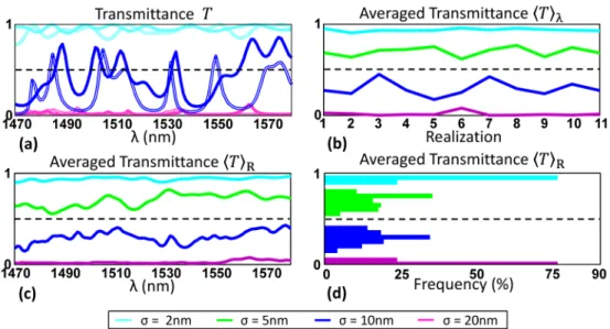
Figure 5(a) shows the transmittance spectrum of the structure for three jitter strengths (σ = 2 nm, 10 nm, 20 nm) and odd jitter, as calculated by 2D F-EEM. Although we simulated 11 different realizations for each σ, for the sake of clarity only two are shown in Fig. 5(a). It is observed that the jitter can dramatically affects the transmittance of a wide SWG waveguide. For σ = 20 nm (10% of the grating pitch), the transmittance is reduced to near zero for the simulated spectral range. For σ = 10 nm (5% of the pitch), the transmittance shows a pronounced wavelength dependence. The influence of the jitter is noticeable even for a jitter strength as small as σ = 2 nm (1% of the pitch), although the effect on the transmittance is much smaller in this case. It can also be observed that two different realizations of the same jitter parameters, i.e. two different structures with the same jitter strength (σ) and type (odd and even) result in substantially different transmittance spectra.
To address this issue of transmittance variations with different jitter realizations and to obtain a quantitative description of the jitter effect, we have defined two types of averages. First, for a specific realization, we define the Wavelength Averaged Transmittance Tλ as:
1 1 (realization ) · ( , realization ), N m n m n T T N λ λ λ λ = =
(1)where Nλ is the number of wavelength points in the spectral sweep.
Second, we define the Realization Averaged Transmittance TR as the mean value of the transmittances for NR different realizations with the same jitter type and strength, for a given wavelength: R R 1 R 1 ( ) · ( , realization ). N n n m m T T N λ λ = =
(2)Corresponding definitions have also been used to calculate the reflectance and the radiation loss averages.
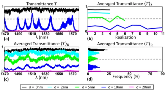
Fig. 5. Calculated transmittance for SWG waveguide structures with odd jitter. (a) Transmittance (T) as directly calculated using 2D F-EEM, for jitter strengths σ = 2 nm, σ = 10 nm and σ = 20 nm. Two different realizations are shown for each value of σ (solid and double line with the same color). Results for σ = 5 nm are not shown here to simplify the visualization. (b) Wavelength averaged transmittance T λ for different realizations, with the jitter strength σ as a parameter. (c) Realization averaged transmittance
R
T wavelength dependence and (d) corresponding histogram for jitters strengths σ = 2 nm, 5 nm, 10 nm and 20 nm.
Figure 5(b) shows the wavelength averaged transmittance T λ for each of the 11 calculated realizations, with the jitter strength σ as a parameter. Interestingly, the curves in Fig. 5(b) resemble those for the averaged transmittance TR dependence on wavelength shown
in Fig. 5(c). This similarity between the two sets of curves is a strong indication that wavelength and realization averaging results converge to each other if the number of samples is large enough. This hypothesis will be validated further in this paper via comprehensive simulations. Finally, in Fig. 5(d) we plot the histograms obtained from the results shown in Fig. 5(c). It is observed that for σ = 5 nm and 10 nm, the averaged transmittance distributions are comparatively broad, which is a consequence of the significant wavelength dependence of the realization averaged transmittance, while when the jitter is substantially reduced (σ = 2 nm) or increased (σ = 20 nm), the distributions are narrow and concentrated near 1 and 0, respectively.
The results presented in Fig. 5 are based on approximately 5000 single-wavelength simulations, which only is practically computationally possible if the problem is solved in 2D, with the structure schematically shown in Fig. 2(b). Although the 2D approximation is expected to be accurate since the width of the segments (W = 3 µm, in lateral dimension, x) is much larger compared to segment thickness (0.22 µm, in transverse direction, y), we also examined the accuracy of our results using a rigorous 3D full-vectorial analysis tool [27]. A comparison between 2D and 3D simulation results is presented in Fig. 6, showing a good agreement between the two, especially for the transmittance curves. This agreement is quite remarkable considering that each point of the 2D curves was obtained as the average of 200 different realizations for a single wavelength, whereas each point of the 3D curves was calculated, for a single realization, as the wavelength average of 61 simulation points within the wavelength range 1.4 µm - 1.7 µm. Therefore, the curves shown in Fig. 6 not only validate the accuracy of our 2D simulations, but they also confirm that wavelength and
realization averages lead to the same results, as previously pointed out. This also means that we can expect statistically significant experimental results by measuring the wavelength response of a comparatively small set of fabricated realizations.
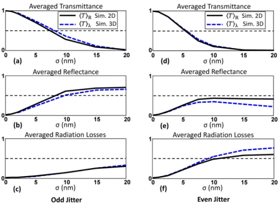
Fig. 6. SWG waveguide transmittance, reflectance and radiation losses, as calculated by 2D and 3D simulations. (a)-(c) Odd jitter, (d)-(f) Even jitter. Each point of the 2D curves is calculated as the average of 200 different realizations for a single wavelength (realization averaged). Each point of the 3D curves is calculated as the average of 61 wavelengths for a single realization (wavelength averaged).
We also studied the influence of the jitter strength and type on the averaged transmittance, reflectance and radiation losses. It was found that even a comparably small jitter produces a significant reduction of the transmittance, as can be seen in Figs. 6(a) and 6(d). This effect is slightly stronger for even jitter than for odd jitter, but in both cases the jitter should be limited to about 2.5 nm or less, for the transmittance T > 0.9. The averaged reflectance grows rapidly for small values of σ, but the curves flatten for large jitter strengths, as shown in Figs. 6(b) and 6(e), while the reflectance is higher for odd jitter compared to even jitter. The input power which is neither transmitted nor reflected is lost by radiation. Our simulations also predict a substantially higher radiation losses for the even jitter compared to the odd jitter, as shown in Figs. 6(c) and 6(f).
4. Experimental results
The jitter effects studied by simulations have been corroborated through comprehensive experimental studies. More than 70 different test structures were fabricated on a silicon-on-insulator wafer with 220 nm Si layer using electron beam lithography and reactive ion etching. A 3- m-thick SiO2 upper cladding layer was deposited using plasma-enhanced
chemical vapor deposition. Broadband and efficient fiber-chip light coupling was achieved with subwavelength engineered mode transformers [3–5]. Since these mode transformers are narrow waveguides with a reduced modal confinement for optimum matching with the fiber mode, they are not substantially affected by jitter, as it will be discussed later in this paper.
Transmittance and reflectance were measured for the nominal design polarization (transverse electric, TE) as a function of wavelength and then normalized using a reference waveguide. Finally, the measurements were averaged to allow for a direct comparison with the simulation results shown in previous section.
Fig. 7. Measured transmittance for different jitter strengths (odd jitter). (a) Raw measurements for: σ = 0 nm, σ = 10 nm, σ = 20 nm. Curves for σ = 2 nm and σ = 5 nm have not been drawn for the sake of clarity. (b) Wavelength averaged transmittance T λ for different realizations. (c) Realization averaged transmittance
R
T as a function of wavelength. (d) Histograms of the realization averaged transmittance
R
T .
For the odd jitter, we fabricated and characterized test structures with jitter strengths σ of 0 nm (4 realizations), 2 nm (4 realizations), 5 nm (6 realizations), 10 nm (11 realizations) and 20 nm (11 realizations). For the even jitter, the following jitter strengths were included: σ = 0 nm (4 realizations), 1 nm (4 realizations), 2.5 nm (6 realizations), 5 nm (11 realizations) and 10 nm (11 realizations). See Data File 1 to find the jitter induced to each period for all the fabricated structures.
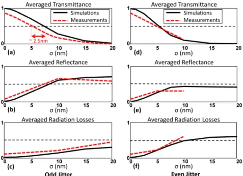
The measured transmittance for the fabricated structures with odd jitter is shown in Fig. 7. A comparison with Fig. 5 reveals a good qualitative agreement, confirming that the jitter influence is critical for wide SWG waveguides. Indeed, in our experiments a small amount of ‘uncontrolled’ jitter inherent to the fabrication process is combined with the intentional jitter, so the actual jitter strength is slightly larger. We have found that the measurements for σ = 0 nm and σ = 2 nm [Fig. 7(c), black and cyan lines] closely resemble the simulations for σ = 2 nm and σ = 5 nm [Fig. 5(c), cyan and green lines], so the uncontrolled jitter floor of our fabrication process can be estimated as σF ~2.5 nm. For our patterning process, consisting of
e-beam lithography with hydrogen silsequioxane (HSQ) resist and reactive ion etching, a root-mean-square line edge roughness of σ∼2.2 nm is expected [28], consistent in magnitude with the considered jitter floor of 2.5 nm.
Simulation and experimental results for both types of jitter (odd and even) are shown in Fig. 8. It is observed that, if we assume the aforementioned jitter floor of 2.5 nm, the agreement is very good, so experimental results validate the main conclusions obtained from simulations: i) even a small jitter noticeably affects the transmittance for both jitter types, ii) the odd jitter exhibits higher reflectance and lower radiation losses compared to the even jitter.
Fig. 8. Jitter influence comparison of simulations and measurements. (a)-(c) Odd jitter. (d)-(f) Even jitter.
Fig. 9. Analysis of the convergence for calculation of averaged values (odd jitter). (a) Averaged measured transmittance, for a single realization, as a function of the wavelength discretization used in the averages. (b) Averaged measured transmittance as a function of the number of realizations used in the averages.
Finally, we have analyzed the convergence rates for the calculation of averaged values as a function of the wavelength discretization [Fig. 9(a)] and the number of realizations [Fig. 9(b)]. From these figures it is clear that, as expected, convergence is slower for stronger jitters. A wavelength discretization Δ = 1 nm (that is, 111 wavelengths within the range [1470 - 1580] nm), assures the convergence to the mean value of the realization under study for all jitter strengths, although a reasonable approximation can be also obtained using coarser discretizations (Δ ~5 nm). On the other hand, for strong jitters different realizations can lead to slightly different wavelength averaged values, [see Fig. 7(b)], so realization average is convenient. If we combine both the wavelength and the realization averages, convergence is achieved using only 3 - 6 realizations even in the case of strong jitters.
5. Discussion
In the previous sections we have studied the effects of the jitter in wide z-periodic SWG waveguides through rigorous electromagnetic simulations and experimental measurements of different (70) fabricated realizations of test structures. Although the development of a comprehensive theoretical framework for the jitter effects is out of the scope of this work, we will suggest some plausible arguments providing physical insight into the problem.
Specifically, we will discuss differences in jitter influence for wide and narrow SWG waveguides, the source of the wavelength dependence in jittered structures, and the rational for the close similarity observed between realization and wavelength averages.
A z-periodic SWG waveguide with jitter can be considered as a superposition of a perfectly periodic SWG waveguide and a perturbed structure, as shown schematically in Fig. 10. Although the exact position and the length of each perturbation depend on the specific realization, its statistics are basically determined by the jitter strength σ. These perturbations produce a coupling between the forward and the backward propagating Floquet-Bloch modes of the unperturbed SWG waveguide. The radiation modes will also be increasingly excited for larger perturbations, resulting in radiation losses.
The amplitude of the backward coupling coefficient at an interface positioned at z = zp
can be approximated as [29]: / 2 2 * 0 / 2 / 2 2 2 0 / 2 ( ) ( , , )· ( , , ) ( , , ) , H W p p W f p b p H W p W f p z n E x y z E x y z dxdy n E x y z dxdy δ δ − − ∝ Δ = Δ
(3)where δp is the perturbation length at the interface z = zp, Δn2 =nSi2 −nSiO2 2 and E(x,y,zp) is the
transverse electric field distribution of the Floquet-Bloch mode at z = zp. Given that both
forward and backward modes have the same transverse electric field distribution, we use Ef =
Eb = E.
Fig. 10. (a) SWG waveguide with jitter is considered as a superposition of an ideal z-periodic SWG waveguide and a perturbation structure. (b) Detail schematic of one of the silicon segments of the structure with a perturbation sheet of length δp located at one of the segment
sidewalls. The coupling strength of the field with the perturbation sheet increases with the waveguide width (W).
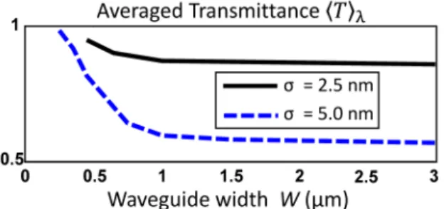
As it follows from Eq. (3), the amplitude of the coupling coefficient depends on the perturbation strength and on the overlap of the two interacting modes at the position of the perturbation sheet [Fig. 10(b), red strip]. For a given pitch and duty cycle, the mode confinement monotonically increases with the waveguide width W, as does the interaction of the field with the perturbation, therefore the jitter influence increases with the waveguide width. This means that the jitter influence is more prominent in wide SWG waveguides compared to narrow Si-wire waveguides. This finding has been validated by numerical simulations, as shown in Fig. 11. For these calculations we have used our 3D full-vectorial analysis tool [27], since for narrow Si-wire waveguides the 2D approximation is not adequate. Two different regions can be identified in Fig. 11. For W < 1 µm the transmittance degrades rapidly with increasing W, as for comparatively narrow waveguides the mode confinement substantially depends on the waveguide width. For W > 1 µm, the transmittance changes only slightly with the waveguide width since for wider waveguides the mode confinement being already high does not change substantially with the waveguide width. These findings also support the following argument why jitter effects have not been discussed in previous works
on SWG waveguides. Most of previously studied SWG structures in silicon waveguides were implemented in narrow (single mode) waveguides, with practically negligible jitter effects. For example, considering an SWG structure with W ~450 nm and 200 grating periods and assuming a jitter strength σ = 2.5 nm, the calculated transmittance is ~0.95.
Fig. 11. Simulated transmittance as a function of waveguide width W. Jitter strengths σ = 2.5 nm and 5 nm. The waveguide length is L = 40 µm (200 periods). Simulations were carried out with a 3D full-vectorial analysis tool [27].
Regarding the wavelength dependent effects observed in wide SWG waveguides, the spectral features in Figs. 5(a) and 7(a) are resulting from destructive and constructive interferences at specific wavelengths, which in turn depends on the sequence of relative phase shifts φ between the perturbations
(
)
FB FB 2
· ·n πλ ,
=d β =d ⋅
φ (4)
where λ is the wavelength, βFB and nFB are the Floquet-Bloch mode propagation constant and
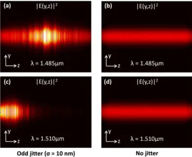
effective index, respectively, and d is the sequence of distances between the perturbations. The sequence of distances d has a random component determined by the sequence of random jitter values δ. Since φ is a wavelength dependent scaling of d, the relative phases also have a random component. Given the relative phase shifts φ also depends on the wavelength, the same realization at different wavelengths can result in very different transmittance and reflectance values. As an example, in Figs. 12(a) and 12(c) are shown simulated electric field distributions at two different wavelengths, yielding high transmittance T ~0.91 for = 1.485 µm and reflectance R ~0.8 for = 1.510 µm, for a waveguide width W = 3 µm and a jitter σ = 10 nm. The electric field distributions corresponding to an ideal SWG waveguide (without jitter) are shown for comparison in Figs. 12(b) and 12(d), for both wavelengths.
Regarding the similarity observed between the realization and wavelength averages, an argument can be made that the wavelength average of a single realization can be construed as an average of Nλ “virtual structures” defined through different phase vectors φ, one for each
wavelength. This is similar to the realization average of NR structures at a single wavelength,
each one defined by a different phase vector φ through a specific jitter sequence δ. This can plausibly explain the close similarity observed between our realization averaged and wavelength averaged results.
Fig. 12. Calculated electric field intensity distributions in an SWG waveguide with jitter. 3-m-wide waveguide with odd jitter σ = 10 nm for (a) 1.485 µm wavelength yielding high transmittance and (c) 1.510 µm wavelength yielding high reflectance. (b), (d) Ideal SWG waveguide (without jitter) for the same wavelengths.
6. Conclusion
The subwavelength grating structures have been used to significantly improve of many state-of-the-art photonic integrated devices, including fiber-chip couplers, evanescent field sensors, multimode interference couplers, wavelength division and mode division multiplexers and Fourier-transform spectrometers, to name a few. In this work we studied for the first time the effects of jitter in z-periodic SWG waveguides by carrying out rigorous electromagnetic simulations and experimental studies. We have found that narrow (single mode) SWG waveguides are barely affected by the presence of jitter while the effect of jitter can be critical in wide (multimode) SWG waveguides. For example, a jitter of 5 nm (2.5% of the pitch) in an SWG waveguide of width W = 3 µm and length L = 40 µm (200 periods), reduces the mean transmittance to ~75% (i.e., about 3 dB loss penalty per 100 µm) while the reflectance is increased to ~25%. Minimizing jitter is therefore critical when working with multimode SWG waveguides. From comparison between simulations and experimental results we have estimated that the uncontrolled jitter floor of our fabrication process is around 2.5 nm, which is sufficiently low to achieve high performance multimode SWG devices (e.g., ultra-broadband MMI couplers [13]). Our study paves the way for successful implementations of multimode SWG-engineered structures in advanced silicon photonic waveguide circuits.
7. Appendix
In the main body of the paper, we have focused on the influence of jitter on the transmission, reflection and radiation behavior of the fundamental Floquet-Bloch mode supported by a wide multimode SWG waveguide with fixed pitch and duty cycle (Λ = 200 nm and DC = 50% respectively), and for a specific number of periods of the test structure (N = 200). In this section, we include a set of additional simulation results that confirm that the obtained conclusions remain valid even if we vary these values. In the following we will keep the waveguide width fixed at W = 3 m, because the impact of waveguide width has already been addressed in Section 5.
Number of periods
Figure 13 summarizes the simulation results obtained when the number of periods varies from N = 50 to N = 300. We have considered here for simplicity only three jitter strengths (σ = 2 nm, 5 nm and 10 nm) and the odd jitter type, although conclusions for even jitter will be similar. As expected, SWG performance degrades with the number of periods. Although this degradation is highly noticeable for strong jitters (e.g. σ = 10 nm), for σ = 2 nm the SWG response is barely affected even if the number of periods grows up to N = 300.
Fig. 13. Analysis of the influence of the number of periods (odd jitter). (a) Simulated wavelength responses for different number of periods (N = 50, 100, 150, 200, 250, 300). (b) Averaged transmittance versus the number of periods. (c) Averaged reflectance versus the number of periods.
Duty Cycle
The effect of the duty cycle (DC) on the transmittance has been also analyzed. We have considered DCs within the range 37.5% - 62.5%, which correspond to a minimum feature size of 75 nm for a pitch Λ = 200 nm. As shown in Fig. 14(a), the averaged transmittance degrades with the duty cycle. This is expected, because increasing the duty-cycle also increases modal confinement and thus the interaction with the perturbation is stronger. This effect is only relevant for strong jitters, whereas for small jitters (e.g. σ = 2 nm) the reduction of the averaged transmittance is much smaller.
Pitch
The simulated averaged transmittance and reflectance curves as a function of the pitch of the SWG waveguide are shown in Figs. 14(b) and 14(c) respectively. The minimum pitch is chosen to yield a minimum feature size of the unperturbed SWG waveguide of 75 nm (Λmin =
2 x 75 nm = 150 nm), whereas the maximum is selected to be just below the Bragg period (Λmax = 270 nm < ΛB ~ 280 nm for = 1.47 m). It can be clearly seen that the curves suffer a
noticeable degradation for pitches greater than 250 nm, which is caused by the proximity to the Bragg regime. Actually, it is well known that SWG structures are highly sensible to fabrication imperfections when the pitch approaches to the Bragg period, so these results are consistent with our expectations.
Fig. 14. Simulated averaged values (odd jitter) as a function of (a) the duty cycle (Λ = 200 nm), (b), (c) the pitch (DC = 50%).
Higher order modes
We have performed a brief study of the effect of jitter on higher order modes. Figure 15 shows the simulated wavelength averaged transmittance for the four guided modes supported by the SWG waveguide (W = 3 m) within the working wavelength range (1470 nm – 1580 nm). It can be seen that transmittance marginally improves with the mode order, which can be expected since higher order modes are slightly less confined and therefore the interaction of the field with the perturbation is marginally reduced.
Fig. 15. Simulated averaged transmittance for the four guided modes supported by a SWG waveguide with W = 3 m (σ = 5 nm, even jitter). Simulations were carried out with a 3D full-vectorial analysis tool [27].
Funding
Ministerio de Economía y Competitividad, Programa Estatal de Investigación, Desarrollo e Innovación Orientada a los Retos de la Sociedad (cofinanciado FEDER), Proyecto TEC2013-46917-C2-1-R, Proyecto TEC2016-80718-R; Universidad de Málaga; Czech Science Foundation, Project No. 16-00329S.
Acknowledgments
![Fig. 1. (a) Geometry of an ideal z-periodic subwavelength grating waveguide (light propagates along the z direction), as first demonstrated in ref [4]](https://thumb-eu.123doks.com/thumbv2/123doknet/14065003.461875/4.918.182.742.310.427/geometry-periodic-subwavelength-grating-waveguide-propagates-direction-demonstrated.webp)