Alternative Chemistries for Etching of Silicon Dioxide and Silicon Nitride by
Simon Martin Karecki
B.S. Electrical Engineering Yale University, 1994
Submitted to the Department of Electrical Engineering and Computer Science in Partial Fulfillment of the Requirements for the Degree of
Master of Science in
Electrical Engineering and Computer Science
at the
MASSACHUSETTS INSTITUTE OF TECHNOLOGY September, 1996
© Massachusetts Institute of Technology, 1996. All Rights Reserved.
Signature of Author
Certified by
Acc nted hv
Department of Electrical Eng7ikeering and Computer Science June 21, 1996
Professor L.Oafael Rei, Thesis Supervisor Department of Electrical Engineering and Computer Science Director, Microsystems Te hology Laboratories, MIT
e---N 1 1 . Chairman, Department
R 0 6 10
9
ithaler adents Fp. JAlternative Chemistries for Etching of Silicon Dioxide and Silicon Nitride
by
Simon Martin Karecki
Submitted to the Department of Electrical Engineering and Computer Science in Partial Fulfillment of the Requirements for the Degree of
Master of Science
in
Electrical Engineering and Computer Science
at the
MASSACHUSETTS INSTITUTE OF TECHNOLOGY
September, 1996
Abstract
At the present time, the etching of dielectric films in semiconductor processing applications relies almost exclusively on the use of perfluorocompounds (PFCs), gases which are suspected global warming agents. The author's research represents the initial stage of a project whose aim is to identify and characterize possible replacements for PFCs in the two principal etching applications: wafer patterning and plasma enhanced chemical vapor deposition (PECVD) chamber cleaning. These processes, which play essential roles in the manufacture of integrated circuits, use and emit perfluorocompounds
in steadily increasing quantities. The scope of the work discussed herein has been to characterize the etch performance of a number of potential replacement candidates for etching silicon dioxide and silicon nitride. The results will be used to screen the candidates for subsequent work, the goal of which will be the development of actual replacement processes for the wafer patterning and chamber cleaning applications respectively. These subsequent stages of this project, portions of which are expected to form the basis of the author's Ph.D. thesis, will build upon the results discussed herein.
A number of potential replacement chemistries from the hydrofluorocarbon (HFC) family has been examined during the course of this work. Statistically designed
experiments and neural network analysis were used to develop empirical models of the etch behavior of these compounds in a commercially available magnetically-enhanced
reactive ion etch (MERIE) tool. Optical emission interferometry was used to measure etch rates in-situ. Films of thermally grown silicon dioxide and stoichiometric chemical
vapor deposited silicon nitride on 100 mm boron-doped silicon substrates were used for this study. A five-level, three-variable central composite design (CCD) experimental matrix was employed to study the dependence of film etch rate on process pressure
(35-150 mTorr), magnetic field strength (0-100 Gauss), and oxygen flow rate (0-20 seem) at constant etch gas flow rates (40 seem) and constant radio frequency power (600 W at
-CFH-CF3), and pentafluoroethane (C2FsH) were studied in this manner, with
octafluoropropane (C3F8), a perfluorocompound, being used as a baseline reference gas. Additional experiments were carried out with these and three other compounds: difluoromethane (CF2H2), 1,1,1,2-tetrafluoroethane (CF3-CFH2), and trifluoroethylene (CF2=CFH). Whereas the first four compounds listed above have been found to etch both oxide and nitride films under all experimental conditions, the latter three have been found to polymerize heavily, depositing what is believed to be a fluoropolymer film, under some of the same conditions. In these latter experiments, a limited study of the effects of oxygen flow rate (0-45 sccm), etch gas flow rate (15 vs. 40 sccm), process pressure (35 vs. 93 mTorr), as well as chamber condition was carried out in a parameter space where polymerization was suppressed.
It was found that 1 H-heptafluoropropane, 2H-heptafluoropropane, and pentafluoroethane etch both films at rates roughly comparable to those of
octafluoropropane under a wide window of conditions. Difluoromethane, 1,1,1,2-tetrafluoroethane, and trifluoroethylene have been found to etch under certain conditions (low etch gas flow rate/low process pressure), though at rates generally lower than those of the remaining gases. Net polymer deposition was found to occur at other conditions with these three gases. On the basis of the results presented in this thesis, from a process performance standpoint, 1H- and 2H-heptafluoropropane and pentafluoroethane appear to show the most promise as etch gases that could potentially be used in wafer patterning and chamber cleaning applications. However, additional work is required to verify that these gases can satisfy all the process requirements of each of these applications. In the case of wafer patterning, anisotropy and selectivity to other materials will be of great importance. Chamber cleaning process conditions, on the other hand, tend to be
considerably different from those in a wafer patterning process. Chamber cleans typically utilize higher pressure, power, as well as gas flows; thus the viability of these chemicals in this different parameter space needs to be explored. Difluoromethane,
1,1,1,2-tetrafluoroethane, and trifluoroethylene may find limited application in wafer patterning, where polymerization mechanisms sometimes play a key beneficial role in obtaining etch selectivity to other films as well as highly directional etch profiles. However, their usefulness in higher pressure chamber cleaning applications which require high etch rates appears to be marginal.
Finally, the compounds examined in this thesis represent only a portion of the potential replacement candidates that will be evaluated as part of the alternative
chemistries project. The evaluation of iodofluorocarbons (IFCs), as well as unsaturated fluorocarbons is also planned.
Thesis Supervisor: Professor L. Rafael Reif
MIT Professor of Electrical Engineering and Computer Science Director of the Microsystems Technology Laboratories, MIT
Acknowledgments
Thanks go out to my parents, for all the sacrifices they have made to get me where I am today, for all the love and encouragement they have given me over the years, and for always believing that one day I might do something worthwhile, like write a thesis, for instance. Thanks
and all my love to Vanessa, for all her patience and understanding, for her never-failing support, for always being there to listen, and -most importantly -for her love and for being a part of my life in so many ways.
Thanks to Professor Rafael Reif, my advisor and the ringleader of our operation, for his leadership and encouragement, for all the advice and guidance, for his confidence in me, and for numerous opportunities to earn frequent flyer miles. Being a part of his research group has truly been a defining experience in my academic life; more importantly, however, it has helped me to grow as a person. I will always be indebted to him. Thanks to Ben Tao, my partner in this project, for his tireless efforts, for his valuable insights, for hours of stimulating discussions, for staying on top of things when the world got hectic, and for his friendship.
Thanks also to Walter Worth, our project manager at SEMATECH, for his support, for his guidance, for being the source of so many invaluable contacts, and for his confidence in our work. And to Dr. Dan Herr, our manager at SRC, for his support and guidance.
To Joe Walsh, Brian Foley, and all the research engineers and staff of the Microsystems Technology Labs for their hard -and often frustrating -work in getting the Precision 5000 up
and running, and -perhaps even more importantly -in keeping it running; for all their help in
times of crisis; and for always being there when their expertise was needed. Thanks also to Bernard Alamariu, Pat Burkhart, and everyone who helped our cause at MTL.
To Linus Cordes, Vicky Diadiuk, Prof. Marty Schmidt, and all those involved in allowing our unconventional processes to enter ICL. To Linus in particular for all his good advice. To Sue Peterson and Sam Crooks at MTL and Paul McQuillan at OSP for making sure that all the important things ran smoothly. Thanks also to Carolyn Zaccaria, Erika Satrape, Diane Hagopian, Kurt Broderick, and Debroah Hodges-Pabon for all their help.
To Igor Tepermeister and Bill Conner at Low Entropy Systems for providing us with the 1000-IS system which proved so valuable in the course of this work, and for their advice and support. Thanks too to Timothy Dalton for his insights and advice, which helped point us in the right direction when the experimental stages were getting underway.
To our SRC Mentors: Avi Kornblit from AT&T (er...Lucent Technologies), Albert Cheng and Charles Lee from TI, and Bruce Huling and Terry Sparks from Motorola. Thanks also to Laurie Beu from Motorola for her advice and encouragement.
To DuPont, for its donation of the NNAPER neural network software which played such a large role in our work, the AEDEPT database, as well as pentafluoroethane and
tetrafluoroethane gases. Many thanks, in particular, to Mike Mocella for all his help and support. Thanks to 3M for their donation of octafluoropropane. Thanks also to Nick Esselman from Applied Materials for his help in answering the many questions we had about the Precision 5000.
To all the members of Professor Reif's research group: Rajan Naik, Weize Chen, and Alex Cherkassky for making my experience here a happy one. (And it's not over yet.)
Thanks to Geo, Tim, and all the staff at Cornwall's, for facilitating my trip around the world, as well as John and Pam, the owners, for allowing me to put some nonsense on a plaque
in their fine establishment. Thanks to Yoshi Uchida and Matt Reagan, for all the stimulating debates on the goods and evils of petrol taxes that were held in the said establishment. To Matt Reagan also for endless hours of X-Files episodes, all the homebrew, and all kinds of
automotive-related advice. I plan to master toe-and-heeling by the time I write my Ph.D. thesis. Thanks to Roger Kermode, Pat Kreidl, Matthew Dyer, and Derek Surka, my housemates, for providing me with such a nice environment in which to take refuge from the world of plasma
etching. Thanks to Chris Conley, for being insane enough to undertake the mammoth 48-hr. cross-continent expedition with me during the writing of this thesis. Thanks to Mark Green, Brian Chen, Karen Willcox, and everyone on Thepack for all the friendship and good times.
Finally, thanks to SEMATECH (Project S69g) and the Semiconductor Research Corporation (Contracts 94-MJ-802 and 95-EJ-802) for their funding of this work.
Table of Contents
Abstract . . Acknowledgments . Table of Contents . List of Figures. List of Tables . 1. Introduction . . . .1.1 Perfluorocompounds in the Semiconductor Industry. . 1.2 Environmental Concerns Associated with Perfluorocompounds 1.3 Overview of the Project on Alternative Chemistries . .
1.3.1 Preliminary Work -Industry Survey and Literature Search
1.3.2 Etch Viability Study . . . .
1.3.3 Wafer Patterning Study ..
1.3.4 Chamber Cleaning Study . . .
2. Fluorocarbons and Plasma Processes . . ..
2.1 Dielectric Films in the Fabrication of Integrated Circuits . 2.2 Glow Discharge Processes -a General Description . .
2.2.1 Sheath Formation . ..
2.2.2 Rf Discharges . . .. .
2.3 Wafer Patterning . . ..
2.3.1 Process Conditions . ..
2.3.2 Dielectric Etching with Fluorocarbon Plasmas .
Polymer Formation ..
Oxygen Effects . . . .
Hydrogen Effects . . . .
F/C Ratio Model and Polymerization . .
Silicon Nitride Etching . .
2.4 PECVD and PECVD Chamber Cleaning .
3. Selection of Candidate Chemistries . . ..
3.1 Selection Criteria . . . ..
3.2 Families of Chemistries to Be Evaluated . . .
3.2.1 Hydrofluorocarbons . . . . 3.2.2 lodofluorocarbons . . . . 3.2.3 Unsaturated Fluorocarbons . . . 3.2.4 Inorganic Fluorides . . .. 4. Experimental Approach . . . . . 4.1 Films . . . ..
4.2 Applied Materials Precision 5000 Etch Tool. . .
.3 .5 .7 .10 .13 S .14 S .14 S .16 S .20 S .21 S .22 S .23 S .24 S .26 S .27 S .28 S .30 S .31 S .36 S .37 S .39 S .40 S .41 S .42 S .44 .45 .46 S .48 S .48 S .49 S .50 S .51 S .53 S .54 S .56 S .57 S .57
4.2.1 Power . . . 59
4.2.2 Pressure . . . .59
4.2.3 Feed Gas Flow Rate . . . .61
4.2.4 Magnetic Field . . . .62
4.2.5 Chamber State. . . .
.64
4.3 Diagnostics: Optical Emission Interferometry . . . .65
4.4 Experimental Plan . . . 68
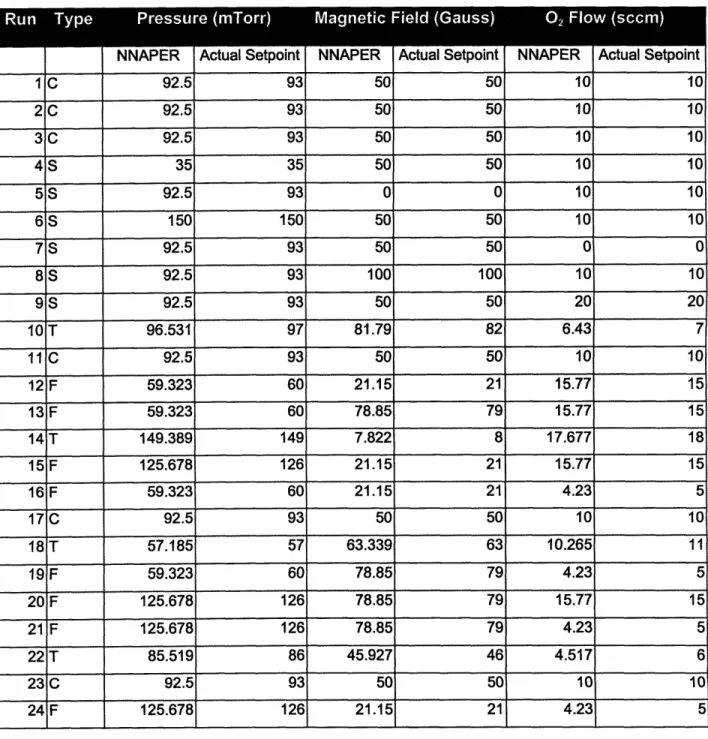
4.4.1 Designed Matrix Experiments -the Central Composite Design .69 4.4.2 Designed Matrix Experiments -Selection of Variables . . 72
4.4.3 Designed Matrix Experiments -Neural Network Analysis . .75
4.4.4 Non-Matrix Experiments . . . .79
Effects of Process Variables on Polymerization . . .81
Oxygen Flow Rate Study. . . . . .81
Supplementary Experiments: Pressure and Etch Gas Flow Effects. . . . .81
Supplementary Experiments: Chamber Condition Effects .82 5. Results and Discussion . . . .86
5.1 Designed Matrix Experiments . . . .86
5.1.1 Octafluoropropane Results . . . .87
Magnetic Field . . . .87
Oxygen Flow . . . .87
Pressure . . . .89
5.1.2 1H- and 2H-Heptafluoropropane Results . . . .91
Magnetic Field . . . .91 Oxygen Flow . . . .91 Pressure . . . .93 5.1.3 Pentafluoroethane Results . . . .94 Magnetic Field . . . .94 Oxygen Flow . . . .94 Pressure . . . .96 5.1.4 Memory Effects . . . .97 5.2 Non-Matrix Experiments . . . .98
5.2.1 Trifluoroethylene Polymerization Study (Non-Matrix Series #1a-d). 98 5.2.2 Oxygen Flow Rate Study (Non-Matrix Series # 2-15) . 103 5.2.3 Etch Gas Flow Rate Study (Non-Matrix Series # 16, 17) . 110 5.2.4 Pressure Study (Non-Matrix Series # 18, 19). . . 112
5.2.5 Memory Effects in Oxygen Flow Rate Studies (Non-Matrix Series # 20-25) . . . 114
5.3 Auger Electron Spectroscopy Data . . . 119
5.4 Summary . . . 120
6. Conclusions and Plans for Future Work . . . 122
Appendix 1: NNAPER Models of Matrix Experiments . 127 Appendix 2: Environmental, Health, and Safety Information on Replacement Candidates 152
List of Figures
Figure 2.1 The potential distribution in a dc diode glow discharge. .. .32 Figure 2.2 Ac voltage waveforms at the generator and at the powered electrode in an
rf diode system. . . . .34
Figure 2.3 An rf diode parallel plate reactor. . . . .35 Figure 2.4 A generic representation of photolithographic pattern transfer. . .36 Figure 2.5 Isotropic vs. anisotropic etch profiles. . . . . .37 Figure 2.6 Fluorine/carbon rations for several fluorocarbon gases. .. .44
Figure 4.1 Schematic of the Applied Materials Precision 5000 platform (System
#6166). . . . .. . . . .58
Figure 4.2 The effect of etch gas flow rate on the etch rate. . . . .62 Figure 4.3 The basics of thin film interferometry as applied in the 1000-IS system. .66
Figure 4.4 The 3 variable, 5 level central composite design matrix. .. .71 Figure 4.5 Preliminary tests with octafluoropropane and 2H-heptafluoropropane on
thermal oxide substrates: oxide etch rate vs. a). 02 flow rate (at 90 mTorr);
b). pressure (at 12 sccm 02 flow). . . . .72
Figure 4.6 Preliminary tests with 2H-heptafluoropropane on thermal oxide substrates: oxide etch rate vs. 02 flow rate without magnetic enhancement. . .73 Figure 4.7 The actual experimental matrix used in this study: a CCD design with a
total of 6 center point replicates and 4 pseudo-random test points
(24 runs total).. . . . .75
Figure 4.8 An example of the three-layer back propagation network used by
NNAPER. . . .
.77
Figure 5.1 Modeled silicon dioxide etch rate in octafluoropropane at 10 sccm 02 flow, showing the shift of the pressure fold-over point toward lower pressures
Figure 5.2 Modeled silicon dioxide etch rate in octafluoropropane at 50 Gauss. The shift ofthe fold-over point toward higher pressures with increasing oxygen
flow is clearly visible.. . . . 90
Figure 5.3 Comparison between the modeled oxide etch behaviors of
1H-and 2H-heptafluoropropane at 35 mTorr. . . . 92
Figure 5.4 Modeled silicon dioxide etch rates as a function of oxygen flow for all four
gases used in the matrix experiments.. . . . 95
Figure 5.5 Modeled silicon nitride etch rates as a function of oxygen flow for all four
gases used in the matrix experiments.. . . . 96
Figure 5.6 Etch rate variation at the center point of the matrix as a function of run
number. . . . 97
Figure 5.7a-d Series # la-d: Effects of pressure (a), magnetic field (b), oxygen flow rate (c), and etch gas flow rate (d) on etch rate/polymer deposition rate on SiO2 with trifluoroethylene as the process gas. . . . . 101-103
Figure 5.8 Series # 2 & 9: Oxide and nitride etch rate in octafluoropropane in the low
flow/low pressure regime. . . . 104
Figure 5.9 Series # 3 & 10: Oxide and nitride etch rate in 1H-heptafluoropropane in
the low flow/low pressure regime . . . 105
Figure 5.10 Series # 4 & 11: Oxide and nitride etch rate in 2H-heptafluoropropane in
the low flow/low pressure regime. . . . 105
Figure 5.11 Series # 5 & 12: Oxide and nitride etch rate in pentafluoroethane in the
low flow/low pressure regime. . . . 106
Figure 5.12 Series # 6 & 13: Oxide and nitride etch rate in difluoromethane in the
low flow/low pressure regime. . . . 106
Figure 5.13 Series # 7 & 14: Oxide and nitride etch/dep rate in
1,1,1,2-tetrafluoromethane in the low flow/low pressure regime. . . 107
Figure 5.14 Series # 8 & 15: Oxide and nitride etch/dep rate in trifluoroethylene in
the low flow/low pressure regime . . . 107
Figure 5.15a,b Series # 16, 17: The effect of etch gas flow rate on oxide (a) and nitride (b)
Figure 5.16a,b Figure 5.17a-c Figures A1.1-6 Figures Al.7-12 Figures A1.13-18 Figures A1.19-24
Series # 18, 19: The effect of pressure on oxide (a) and nitride
(b) etch/dep rate. . . . 113, 114
Series # 20-25: Memory effects with trifluoroethylene: oxide runs (a, b) and nitride runs (c). . . . . 115, 117, 119
Octafluoropropane NNAPER model results.. 2H-heptafluoropropane NNAPER model results. 1H-heptafluoropropane NNAPER model results. Pentafluoroethane NNAPER model results. .
127 134 140 146
List of Tables
Table 1.1: 1993 U.S. Semiconductor Industry PFC Purchases . . . . 15 Table 1.2: Etch Applications of Perfluorocompounds . . . . .16
Table 1.3: Properties of Greenhouse Gases . . . .18
Table 3.1: Properties of Selected HFCs . . . . 50
Table 3.2: Properties of Selected IFCs . . . 51
Table 3.3: Properties of Selected Unsaturated Fluorocarbons . . . .53 Table 3.4: Health/Safety Issues Associated with Selected Inorganic Fluorides . .55
Table 4.1: NNAPER Experimental Matrix . . . 78
Table 4.2: Summary of Matrix Experimental Series . . . 79
Table 4.3: Fluoropolymer Deposition Rates for C2F3H and C2F4H2 Measured at the
Matrix Center Point . . . 80
Table 4.4: Summary of Non-Matrix Experimental Series . . . . 84
1.
Introduction
The goal of the research presented in this work is the development of alternatives to an environmentally harmful class of substances used in semiconductor manufacturing known as perfluorocompounds. This introductory chapter will review the role that perfluorocompounds play in the semiconductor industry (Section 1.1), discuss the nature of their environmental
impact (Section 1.2), and outline the means through which the author's research is intended to play a part in developing a solution to this problem (Section 1.3).
Chapter 2 will attempt to provide a brief overview of the processes in semiconductor manufacturing in which perfluorocompounds are employed. Chapter 3 will discuss the selection
of the chemistries that are being considered as replacements for perfluorocompounds in these processes. It will also discuss the properties of the compounds that have been selected. Chapter 4 will be devoted to the details of the experimental procedure that was used. The results of the
experiments conducted with alternative chemistries will be presented in Chapter 5. Finally, Chapter 6 will provide some concluding thoughts.
1.1
Perfluorocompounds in the Semiconductor Industry
Perfluorocompound (PFC) chemistries are widely employed as process gases in the semiconductor industry. Their principal application in integrated circuit manufacture is as feed gases in plasma etching processes: patterning of thin films and in-situ cleaning of plasma enhanced chemical vapor deposition (PECVD) chambers. A discussion of these processes, as well as of the role of plasma discharges will be deferred until Chapter 2. A loose working definition of a "perfluorocompound" is a fully fluorinated molecule, i.e., one which has all its bonds saturated with fluorine. As a practical matter, most, though not all, of the compounds currently grouped under this umbrella term are fully fluorinated halocarbons. Unsaturated
fluorocarbons, e.g., C2F4 (CF2=CF2), are not considered PFCs, whereas the perfluoroalkanes, e.g., C2F6 (CF3-CF3) are. PFCs have been found to be effective etchants since they are rich sources of
fluorine. Moreover, certain PFCs, namely fully fluorinated halocarbons, possess additional properties that are highly desirable in wafer patterning, such as the potential to form a passivating film in an etching environment. Furthermore, generally speaking, the compounds classified as
PFCs are stable, non-flammable, and (with the exception of NF3) non-toxic, all of which further enhances their desirability from a process standpoint.
However, PFCs are considered to be very potent global warming gases, as will be discussed in the following section. Thus their use and emission represent an area of concern for the semiconductor industry. Currently, tetrafluoromethane (CF4), hexafluoroethane (C2F6), sulfur
hexafluoride (SF6), nitrogen trifluoride (NF3), and more recently octafluoropropane (C3F8), are
the PFCs most heavily used in integrated circuit fabrication. Trifluoromethane (CHF3), though not strictly a perfluorinated compound, is also a heavily used etchant that shares the same environmental concerns as the PFCs, and is therefore treated as one for practical purposes (see Table 1.3).
PFCs can be used to etch a variety of materials: polysilicon, dielectrics (i.e., silicon dioxide, SiO2, and silicon nitride, Si3N4), as well as refractory metals (i.e., tungsten). Silicon dioxide and silicon nitride patterning and chamber cleaning, however, account for the largest share of PFC usage/emission in semiconductor manufacturing [2]. Of this share, chamber cleaning processes use the larger portion of PFCs. This is in part due to larger gas flows (liters per minute versus cubic centimeters per minute) and longer process times. Table 1.1 shows data released by SEMATECH on 1993 levels of U.S. semiconductor industry PFC purchases. Of the four principal gases included in the study, CF4 and SF6 find application primarily in wafer patterning, whereas C2F6 and NF3 are used principally for chamber cleaning. It can be seen,
therefore, that chamber cleaning usage does account for larger amounts of PFC purchases. This application, moreover, is reported to be the faster growing one in terms of volumes of gas consumed [2]. Nevertheless, wafer patterning still accounts for a very significant share.
Table 1.1: 1993 U.S. Semiconductor
Industry
PFC Purchases [1]
Estimated U.S. Total (in metric tons)
67
177
18
45
307
%
of Total
22
58
6
14
100
I
As Table 1.2 shows, dielectric films are exclusively dependent on PFCs, while tungsten and polysilicon etch processes are not. As will be discussed in a later section, Section 2.3.1, the only halogen specie which is effective at etching silicon nitride and oxide films is fluorine. Moreover, presently, the only industrially accepted means of delivering fluorine to the etch process is via a PFC feed gas.
Table 1.2: Etch Applications of Perfluorocompounds [2]
Silicon patterning C2F6, SF6, NF3, CF4, BCl3, HBr, Cl2, HCI
SiO2
patterning
C2F6, SF6, OF4, CHF3 Si3N4 patterningOF
4, C2F
6, SF6,CHF
3Tungsten patterning SF6, NF3, C12
Si0
2and SiNx PECVD chamber cleaning C2F6, NF3, SF6,CF
41.2
Environmental Concerns Associated with Perfluorocompounds
The reason behind the increased scrutiny that PFCs have received in recent years is the role they are suspected of playing in global warming. Global warming is defined as an
augmentation of what is known as the natural greenhouse effect through anthropogenic means. A succinct explanation of the greenhouse effect is given in [3, 6]. Essentially, little of the incoming solar radiation (which is predominantly in the "shortwave" -visible and UV -regions of the spectrum) is absorbed by the atmosphere. Approximately one third of it is reflected back into space by clouds, the air itself and atmospheric particles (which scatter the incoming light), as well as by the earth's surface. The remainder of the incoming energy is absorbed by the earth's surface, which warms up and emits some of it as "longwave" (IR) radiation. Without this re-emission, the earth's surface temperature would increase continuously. Whereas visible and UV radiation is not readily absorbed by atmospheric constituents, infrared radiation is. Thus a substantial portion of the outgoing IR emissions is trapped by naturally occurring gases in the atmosphere -mainly water vapor, but also carbon dioxide (CO2), methane (CH4), nitrous oxide
(N20), and ozone (03). These atmospheric constituents then re-emit this trapped energy, approximately half of which escapes into space, while the other half is emitted toward the surface, thus warming it. It is important to remember that, in an unperturbed state, the net outward flux of energy would balance the net incoming flux.
A perturbation in the balance between incoming and outgoing radiation is defined as radiative forcing. A radiative forcing effect (a change in outgoing IR radiation from the earth) can thus be attributed to a given gas, which, when present in the atmosphere, absorbs IR radiation and re-emits it toward the surface. The concept of radiative forcing is used to define global warming potential (GWP), a metric by which greenhouse gases, whether naturally occurring or anthropogenic, may be compared. This index is a measure of the time-integrated increase in radiative forcing resulting from an instantaneous release of a unit mass (1 kg) of a given compound in today's atmosphere, relative to that from 1 kg of carbon dioxide [4], which is nominally assigned a GWP of 1. This is quantified in the following equation [5]:
f aicdt
G WPT =,
faC
0c co2
dt
where ai is a coefficient quantifying the instantaneous radiative forcing that results from a unit increase in the atmospheric concentration of a given gas i, ci is the concentration of that gas in the atmosphere as a function of time, and T is the integration time, i.e., the time after the release through which the calculation is being performed. Typically GWPs are listed for 20, 100, and 500 year time horizons, with the 100 year value being used most commonly. Gases for which GWP values have been calculated include CO2, N20, methane, as well as a number of
halogenated compounds, among them PFCs [6].
While present day models of the earth's climate and temperature records taken over the course of the last century do not irrefutably substantiate the existence of a global warming trend, there is substantial evidence for increased concentrations of stable, infrared absorbing gases such as CO2 and halocarbon compounds in the atmosphere [3,6]. According to the Intergovernmental
Panel on Climate Change (IPCC), if total emissions of global warming gases continue at present levels, the consequences could be an increase in global mean temperature by 0.3 oC per decade (which would not be uniformly distributed but rather relatively small at equatorial latitudes and
large in polar regions [3]) and a rise in the global mean sea level of about 6 cm per decade [5].
An increase in total rainfall (which would again not be favorably distributed) is also predicted
[3].
PFCs are thought to be potent global warmers because of a confluence of two properties: high stability (and therefore atmospheric longevity) and excellent infrared absorbency [6]. This
combination results in long-lived species that are very efficient at trapping and re-emitting longwave radiation emitted by the Earth's surface. A measure of the atmospheric persistence of a compound is its atmospheric lifetime, defined as the exponential decay constant for an
atmospheric concentration of that species. (I.e., the lifetime is the time in which a concentration of a given substance is projected to decay to 1/e or -37% of its initial value.) The calculated atmospheric lifetimes of some of these substances are as high as thousands or tens of thousands of years [6]. Since GWP is a function of both the atmospheric longevity (which manifests itself through the time-dependent coefficient ci in the above equation) and the infrared absorbency of a compound, it is not surprising that perfluorocompounds possess very high GWPs (see Table 1.3).
Table 1.3: Properties of Greenhouse Gases
(yas) (0 Yr Inerae Time oizn
CF4 02F6 C3F8 SF6 NF3 CHF3 CO2 50,000 10,000 5,600 3,200 740 390 50-200 12,500 6,950 24,900 8,100 12,100 1
All from [6], except C3F8 [7, 8], and CHF3, NF3 [9].
The use of PFCs in semiconductor processing is problematic for a number of reasons. Many process tools which use these substances have low "conversion efficiencies;" that is, most of the influent feed gas is not reacted and consequently becomes part of the exhaust. While conversion efficiencies as high as 80-90% have been reported for NF3in some chamber cleaning
processes, figures as low as 10-15% have been found for CF4. The PFC used in largest
quantities, C2F6 has typical conversion efficiencies of 30-40%. [1, 8, 9] Moreover, because these
chemicals are so stable, they pass unscathed through the water scrubbers commonly placed on exhaust lines at fabrication facilities [1]. Their stability also makes them difficult to abate through combustion [2].
Presently, PFC usage, and hence emission, in the semiconductor industry is increasing rapidly. This rise stems from a number of reasons, including larger numbers of wafers being processed, greater complexity of processing sequences, which results in an increase in the number of processing steps requiring PFCs, and an overall shift from wet chemical processing toward dry (gas phase) processing, which results in the use of PFCs in new applications [1].
While no regulatory driver -domestic or international -presently exists to mandate
reductions in PFC emissions, the emergence of regulatory protocols regarding PFCs is a
possibility. Most present anthropogenic greenhouse gas emissions are in the form of gases such as CO2 and, to a lesser extent, N20 and CH4 [6]. Consequently, the initial focus of international
attention by bodies such as the United Nations Conference on Environment and Development, which produced the "Framework Convention on Climate Change" in 1992 [10], has been on addressing CO2 emissions. PFCs, however, are coming under increased scrutiny because of their
alarming potency and the relative permanence of their effects. For instance, the 1993 U.S. Climate Change Action Plan, which serves as a policy blueprint for regulatory agencies such as the EPA, specifically calls for reductions in the emissions ofhalogenated compounds, including PFCs [ 11 ]. The EPA is, in fact, presently entering into voluntary agreements with various PFC-emitting industries, including the semiconductor industry, that are aimed at achieving emission reductions. A Memorandum of Understanding addressing PFC emissions has been negotiated between the EPA and various semiconductor manufacturers. A number of companies have already signed this agreement, which, among other terms, commits the signatories to (company-blind) reporting of estimated PFC emissions to the EPA on an annual basis, and striving to reduce their PFC emissions (as normalized to a common unit of production) through process optimization, recycling/abatement, and/or chemistry replacement [12]. In addition to
governmental pressure, there are other pressures on the semiconductor industry to reduce PFC emissions, most notably DuPont's sale policy on Zyron- 16 (C2F6), which will phase out the
supply of C2F6 by DuPont if solutions to reducing emissions of this PFC are not sufficiently
mature by year-end 1999 [13].
There are presently several possible avenues which can be followed in an attempt to reduce PFC emissions. These include: process optimization, emission abatement through thermal or plasma destruction, and recovery/recycle. The reader is referred to [14] for an
overview of these options. Arguably the most forward-looking solution for the long term, however, would be the replacement of PFCs with compounds that are more environmentally benign. The National Technology Roadmap for Semiconductors has targeted the year 2007 as the date that PFC replacements should be available [15]. The work described in this thesis is intended to facilitate reaching that goal.
1.3 Overview of the Project on Alternative Chemistries
The work that has been performed to constitute the basis of the author's Master's thesis is part of a larger, multi-year program at MIT, whose goal is to provide industrially acceptable
long-term solutions to the PFC problem. This work is presently funded by SEMATECH, the semiconductor industry consortium, through a Semiconductor Research Corporation contract under the title "Alternative Chemistries for Wafer Patterning and PECVD Chamber Cleaning." The author's Master's thesis will present results from the initial stage of this project, whose aim is the development of viable alternatives to the PFC-based etching chemistries that are used in both wafer patterning and PECVD chamber cleaning. An experimental plan for all stages of this project, which is expected to span a total of three to four years, has been formulated. As an overview, an outline of this plan, including descriptions of subsequent stages that are expected to form the basis of the author's Ph.D. thesis work, will be presented below. A more detailed description of the initial stage of this project, along with a discussion of the results obtained to date will form the body of this thesis.
The etching of two types of dielectric films, silicon dioxide and silicon nitride, is being investigated. Since the end objective of the project is eventual transfer of technology to
semiconductor equipment vendors, it is planned that all stages of the project will be carried out in commercially available, rather than experimental, process tools. An Applied Materials Precision 5000 MERIE (magnetically enhanced reactive ion etcher), presently housed in the Integrated
Circuits Laboratory that is part of the Microsystems Technology Laboratories at MIT, has been used for the work described in this thesis. The Precision 5000 is a widely used commercial etch tool* that is in many ways representative of the current level of commercially available
technology.
1.3.1 Preliminary Work - Industry Survey and Literature Search
Prior to the inception of the experimental work, a survey of industry process and ESH (environment, safety and health) professionals and a search of literature were conducted by the author's coworkers (B. A. Tao, L. R. Reif). This was done in an effort to obtain basic
information on semiconductor industry PFC usage as well as its research needs in this area. Along with this, an attempt was made to determine what non-perfluorocompound gases, if any, had previously been examined in the role of dielectric etchants, both in industrial and R&D settings. In brief, a determination was made 1). that the development of alternatives for both wafer patterning and chamber cleaning processes should be pursued and 2). that the scope of the work should be properly restricted to those processes in which the development of alternatives can make the largest impact, namely dielectric film patterning and dielectric PECVD chamber cleaning. As had been mentioned earlier (Section 1.1), these processes use PFCs most heavily and are moreover exclusively dependent on PFCs, i.e., no production-worthy alternatives are presently thought to be available. While a number of fluorinated compounds besides PFCs had been identified as having been used to etch dielectric films, most were rejected from
consideration for this study due to either extreme handling hazards (e.g., CIF3, BrF3, BrF5, IF5,
anhydrous HF, F2), lack of known suppliers (S2F2), or excessive cost (XeF2). For a more
extensive account of the findings of the industry survey/literature search, see [16]. The present list of candidates was drawn from a large database of halogenated compounds which was created after the completion of the search/survey. The criteria according to which the candidates were selected as well as properties of the selected compounds are discussed in Chapter 3.
* It should be pointed out that, although the terms "etching" and "etch process" have thus far been used generically
in this thesis to describe processes which involve the removal of a film, whether it is in a wafer patterning or a chamber cleaning application, it is common practice to use these terms interchangeably with "wafer patterning." Thus an "etch tool" or an "etcher" refers to a process tool that is dedicated to a wafer patterning application.
1.3.2 Etch Viability Study
The initial stage of the project is an "etch viability" stage, during which a large number of potential replacement chemistries are being tested for etch performance relative to a
perfluorinated etchant. Even though this work is being performed in a process tool used for wafer patterning, the experiments carried out during this stage are intended to be simple enough to be generic to both intended applications (wafer patterning and PECVD chamber cleaning). They are also intended to serve as a method for screening the candidate chemistries. Subsequent stages will address the wafer patterning and the chamber cleaning applications separately. These stages will use a smaller subset of the chemistries initially examined. These will be selected largely on the basis of results from the initial stage.
The primary focus of this first stage has been to determine under what conditions, if any, a given candidate chemistry will etch silicon dioxide and silicon nitride. As will be discussed in detail in Section 3.2, three families of chemistries have been selected as potential candidates to be examined: hydrofluorocarbons (HFCs), iodofluorocarbons (IFCs), and unsaturated
fluorocarbons. This thesis will discuss experimental results from work carried out with the hydrofluorocarbon family. Six gases: 1H-heptafluoropropane (CF2H-CF2-CF3),
2H-heptafluoropropane (CF3-CFH-CF3), pentafluoroethane (C2FH), difluoromethane (CF2H2), 1,1,1,2-tetrafluoroethane (CF3-CFH2), and trifluoroethylene (CF2=CFH) have been evaluated, with the PFC octafluoropropane (C3F8) being used as a baseline reference. The remaining families of candidate chemistries will be evaluated at a later date.
Etch rate was the principal variable of interest. Blank (unpatterned) thermally grown oxide and LPCVD (low pressure chemical vapor deposition) stoichiometric nitride films were etched. 100 mm boron-doped silicon substrates were used. Etch rate measurements were taken
in-situ using optical emission interferometry (OEI), a technique developed by Dalton, et al [17].
Statistically designed experiments and neural network software were employed to formulate empirically derived etch behavior models for some of the gases. The principal process parameters whose effects were studied were process pressure, magnetic field strength, and oxygen flow rate. The effects of feed gas (etchant) flow rate and chamber condition were also studied. Section 4.2 contains a more detailed discussion of the role of each of these process parameters in the Precision 5000.
1.3.3 Wafer Patterning Study
Once the initial pool of candidate alternatives has been benchmarked for etch
performance, separate experimental procedures will be followed for the wafer patterning and PECVD chamber cleaning aspects of the project. It is likely that, because process requirements
in the two applications are quite different, the subset of gases used and the solutions that will emerge for each will be different.
The criteria for evaluating the performance of a wafer patterning process are numerous, but four primary parameters which are of fundamental importance in this application are etch rate, uniformity, selectivity, and anisotropy (vertical directionality of the etch). Among other important considerations are loading effects, substrate damage, residual contamination on the wafer, particle generation, wafer-to-wafer process drift, and hardware compatibility, e.g., chamber corrosion or pump oil degradation. The goal of this stage will be to develop effective alternative chemistry etching processes for silicon dioxide and nitride, as defined by the above criteria. The same etch chamber on the Precision 5000 as in the first stage will be used. Thermal oxide and LPCVD nitride films will again be used. Wafers will be patterned with masks
containing generic structures of varying dimensions. Different features, such as lines, rectangles, and other geometrically simple structures, in both dense and isolated patterns, will be etched. Etch rates and uniformity will be determined in-situ using OEI. The measured etch rates will be used to determine selectivities between the dielectric films and silicon, between the dielectric films and photoresist, as well as between the two dielectric films themselves. Anisotropy will be measured using scanning electron microscopy (SEM). Measurements of fluorine concentration in the plasma will be taken using optical emission spectroscopy (OES). An argon actinometry technique will be used. Concentrations of other species of interest, e.g., CF, CF2, may also be
measured using actinometry. Auger electron spectroscopy (AES) and/or X-ray photoelectron spectroscopy (XPS) will be used to analyze any surface residues that may form. As a final test of the viability of a given etch process, devices and possibly circuits such as ring oscillators may be fabricated using the alternative process. These will then be compared against the performance of similar devices and circuits made using a standard PFC-based etch chemistry.
One of the most important diagnostics in this stage, however, will be effluent
mass spectroscopy (QMS). Even when gases which themselves pose no short- or long-term environmental hazards are used, undesirable products may be formed in the process chamber. A
concern particular to carbon/fluorine chemistries is the possibility of perfluorocarbon formation in the plasma phase through the recombination ofF atoms and CFx fragments. For instance, it has been shown [8] that in processes which utilize larger perfluorocarbon species, e.g., C2F6 and
C3F,, a substantial fraction of the effluent is in the form of CF4. A process recipe which produces significant amounts of perfluorocarbons is clearly undesirable. Monitoring the composition of the effluent stream will therefore be a critical aspect of the study.
1.3.4 Chamber Cleaning Study
In this stage of the project, a smaller subset of the chemistries evaluated in the initial stage will be used to develop an effective process for cleaning dielectric PECVD chambers. This subset will not necessarily be the same as that to be used in the wafer patterning experiments. The reason for this is that the process requirements for chamber cleaning are different and, in general, simpler than those for patterning. In chamber cleaning, the principal parameter of interest is cleaning time, i.e., etch rate. Selectivity and anisotropy considerations as defined
above are, generally speaking, not important. Etch rate and chamber clean time will be measured as a function of process parameters such as rf power, total pressure, and fluorocarbon and oxygen flow rates.
A Novellus Systems Concept One PECVD tool or possibly a PECVD chamber to be installed on the Precision 5000 will be used. (The Precision 5000 platform is capable of serving a dual etch/CVD role.) Typical chamber cleans in PECVD reactors consist of two steps -a high pressure electrode/susceptor clean and a low pressure remote surface clean. Both two step and single step cleans will be performed. Wafer fragments with PECVD oxide or nitride will be placed in various locations in the chamber to monitor the etch rate as a function of location. The etch rates will be measured ex-situ using Nanospec®. For all experiments, a deposition process will be performed in the chamber before the cleaning process is run. This pre-coating of the chamber is necessary when wafer fragments are used to avoid loading effects. Additionally, the effectiveness of the cleaning recipe will be measured by the time it takes for the chamber to be cleaned, as determined by OES endpoint detection, a common technique which identifies process
endpoint by recording the change in an emission line from the plasma (typically a fluorine
emission line for PFC processes). OES will once again be used to measure concentrations of key species in the plasma. Finally, effluent characterization will be performed using FTIR and possibly QMS.
2.
Fluorocarbons and Plasma Processes
The goal of this chapter will be to serve as a preface to later discussions of
hydrofluorocarbon etching of dielectrics. The chapter will thus be devoted to reviewing, by way of background, the role of dielectric films in microelectronic fabrication (Section 2.1) and the salient features of plasma discharges in general (Section 2.2). While this latter discussion is not meant to be exhaustive, some key aspects of plasma discharges will be discussed at length
-albeit only in first-order detail -in order to present the reader with a reasonably accurate physical picture of the environment that is present in the process chamber during the etch process. This will pave the way for a discussion of the roles of specific process parameters in the Precision
5000 etch tool that was used for the work in this thesis (Section 4.2). The general section on glow discharges will be followed by an overview of the etching of dielectric films in the plasma applications of: wafer patterning (Section 2.3) and PECVD chamber cleaning (Section 2.4). Both of these processes involve the removal of a film through chemical reactions with species
generated in a non-equilibrium plasma discharge. An additional component resulting from the bombardment of the etched surface by energetic ions generated by the plasma may also play a key role, depending on the tool configuration and process conditions. As will be seen later, many etch processes, particularly those used for wafer patterning, in fact rely on a synergistic
effect between the chemical and physical etch components. (There exists a still different class of etch processes involving plasmas -"sputter etching" -in which films are removed solely through physical bombardment by energetic ions. These processes, however, will not be discussed here.) Qualitatively speaking, the same etch chemistries may be used to remove the same types of films in both the wafer patterning and the chamber cleaning applications. However, the two applications differ not only in purpose, but also in the process conditions present, the nature of the films being etched, as well as the etch mechanisms themselves. These two applications, along with PECVD itself, represent the major uses of plasma discharges in semiconductor manufacturing. While little attention has been devoted to systematic studies of etching in the chamber cleaning application, there exists a large body of literature, generated by both industry and academia, on plasma wafer patterning processes as well as PECVD. The foregoing chapter will not attempt to review this body of literature, but will instead provide a working description
of plasmas and plasma etch applications, with particular attention to the use of fluorocarbon compounds in the etching of dielectric films.
2.1
Dielectric Films in the Fabrication of Integrated Circuits
The manufacture of integrated circuits is a complex sequence of processing steps. As of this writing, fabrication of advanced integrated circuits may involve more than six weeks of processing and over 100 individual process steps [18]. Integrated circuit manufacture will not be reviewed here, as the reader may be referred to any of a number of excellent textbook sources which give detailed descriptions of typical fabrication sequences [19, 20, 21, 22].
However, it will be pointed out that dielectric films are ubiquitous throughout the structure of a typical IC. For the purposes of this discussion, the term "dielectric films" will be restricted to silicon dioxide and silicon nitride -the two most prevalent types of films, though by no means the only ones used in ICs. In a typical MOS (metal-oxide-semiconductor) system, the many uses of thermally grown silicon dioxide films include gate dielectrics, field insulation between devices, and implant or diffusion masking layers, just to name a few [23]. Deposited silicon oxides are grown via either low pressure chemical vapor deposition (LPCVD) or plasma enhanced chemical vapor deposition (PECVD). Among the uses of these films are: insulation between polysilicon and metal layers, insulation between metal layers in a multi-level metal structure, diffusion sources (when doped), masking layers, and an array of other applications [24,
25]. Silicon nitride, which is deposited through either LPCVD or PECVD, is also widely employed in ICs as: barrier layers, masking layers, passivation, blanket etch stop layers, as well as a number of other applications [26, 27]. The above list is by no means exhaustive and new variations on the uses for oxide and nitride films are constantly being developed. What is clear, however, is that, as device complexity increases, the number of process steps requiring the patterning of oxide and nitride layers will increase, as will the number of steps requiring the deposition of these films through CVD, which will in turn require the cleaning of the deposition chambers. Hence all trends point to ever increasing PFC usage and emission. It should be pointed out here that, while plasma chamber cleaning is commonly associated with the removal
of residue films in plasma enhanced CVD chambers, the use of plasmas in cleaning steps has more recently been applied to tube furnaces as well.
2.2
Glow Discharge Processes - a General Description
A plasma, generally speaking, is a partially ionized gas in which the charged species have sufficient concentrations to interact through Coulombic collisions [28]. These charged species are electrons and ionized molecules and atoms. One can broadly differentiate between two types of plasmas. The first is an equilibrium plasma, where the temperatures of the ions and the
electrons are equal -examples include the sun and arc welder discharges. What is known as a "plasma" in semiconductor processing usage is actually the second type, described more accurately as a glow discharge, or a type of non-equilibrium plasma. In such a discharge, the electron temperature is higher than the ion temperature. In a glow discharge used in an IC fabrication application, a typical value for the ion temperature may be 500 K (0.04 eV), while a typical value for the electron temperature may be 23,000 K (-2 eV); in the absence of external heating or cooling of the chamber containing the discharge, the neutrals in the discharge tend to remain close to room temperature [29].
A glow discharge is sustained by the introduction of energy via an electric or magnetic field. Electrons respond rapidly to the applied field, accelerating to high energies relative to those of the more massive ions and neutrals around them. Because of the large difference in mass between the electrons and other species in the discharge, little energy is lost by the
electrons in elastic collisions with other particles. This means that the electrons remain energetic enough to produce significant amounts of, ions, free radicals, and other excited species through inelastic collisions with the neutrals. However, since little energy is exchanged between the population of electrons and those of other species, there is little heating of the gas in the
discharge, which offers the significant advantage of allowing processing to be performed at low temperatures. [28, 30]
The gases employed in this study are all believed to generate "electropositive" plasma discharges, i.e., the more common type, where the dominant negatively charged species are electrons and where negative ion populations are negligible. A second class -so-called
"electronegative" discharges -exists. Representative members are plasmas generated by NF3 and SF6. In these plasmas, negative ions are believed to form a dominant portion of the negative
species [31], which has complex repercussions on the electrical properties of the discharge. The discussion in this thesis, however, will be limited to electropositive plasmas.
The majority of plasma process tools -whether they are used for wafer patterning or PECVD -that are in use today are so-called "low density" plasma tools, where power is
capacitively coupled to the discharge through a radio frequency signal, typically at 13.56 MHz. The most common configuration in such tools is the parallel plate "diode." A schematic
representation of an rf diode system is shown in Figure 2.3. Process conditions such as applied rf power, pressure, and gas flow rates differ widely between applications and between different tools. Ranges for these parameters in representative etch and PECVD tools will be given in
subsequent sections. Collectively, low density plasmas can be characterized by having plasma
(i.e., electron and ion) densities on the order of 109 - 1011 cm' and ionization fractions on the
order of 106 - 10-' [30, 32]. This is in contrast to "high density" etch or PECVD tools, which may use inductively coupled rf power input or microwave frequency (2.45 GHz) power input. These tools achieve plasma densities of 1010 - 1012 cmf3 and attain ionization fractions of 10-4 to
101, i.e., as high as 10% [32].
At the present time, there exists a consensus that future generations of plasma tools for dielectric patterning and film deposition will, in all likelihood, incorporate high density sources. This technology, however, is still not at a mature stage of development. In addition, it does not appear that all future generation processes will require the advantages of finer control over the conditions seen by the wafer and greater efficiency that high density tools provide. At present, conventional (low density) plasma tools are projected to continue to meet many of the needs of the industry in dielectric deposition and etch for years to come [33, 34]. Furthermore, currently installed low density tools, which presently continue to form the bulk of the installed base of plasma process equipment, have projected lifetimes of ten to fifteen years [33,34]. Thus, the focus of the alternative chemistries project will be on low density tools. The intent will be to demonstrate the viability of replacement chemistries in commercially available equipment.
Before moving on to a discussion of the processes of wafer patterning and PECVD chamber cleaning, some detail needs to be added to the description of the discharge in a plasma tool. The bulk of the plasma is always the most positive region in the system. This region, which typically fills most of the space between the electrodes, glows brightly due to the continuous deexcitation of excited species by photon emission. This is also the region where
most of the ionization and dissociation processes occur. This region is, to first order, field free and thus quasi-neutral. Electron and ion densities in the bulk are nearly equal, and are thus characterized by the single parameter -plasma density. Any surface that the plasma wets is at a lower potential than the bulk, hence an electric field exists at all surfaces wet by the plasma. The regions between the plasma bulk and electrodes and other reactor surfaces are called sheath regions. These regions are dark, indicating little excitation activity.
2.2.1 Sheath Formation
The reason why the plasma bulk is the most positive region in the system ultimately stems from the fact that electron and ion masses are very different. Sheath formation can be explained by the fact that the lighter electrons can acquire greater energies in response to applied fields and hence can diffuse out of the plasma bulk much more readily than ions. For a more detailed discussion of the following, the reader is referred to [35]. When a plasma is first struck, the walls of the chamber are electrically neutral. To use a simple example, one can visualize
sheath formation in a dc discharge at an electrically isolated (floating) surface, designating Vf as the potential of this surface relative to ground and Vp as the potential of the plasma bulk relative to ground. If an electrically isolated surface is exposed to a plasma, initially the electron flux is much larger than the ion flux because the mean electron velocity is much larger than the mean ion velocity. The surface thus builds up a negative charge, which repels incoming electrons and decreases the electron flux. (The ion flux is not increased because it is limited by the arrival rate of ions at the interface of the plasma with the sheath that is being formed, whereas the electrons are being decelerated, which prevents the slower ones from reaching the surface altogether.) Since the voltage at the surface Vf is such as to repel electrons, it follows that Vf< Vp and that the sheath potential (Vp - Vj) > 0.
The ion and electron fluxes entering the sheath at a floating surface wet by the plasma are:
S4 e 4e
respectively, where ne = ni = the plasma density, and ci and -e are the mean velocities of the ions and the electrons in the plasma. (These velocities are not the classical mean square speeds,
given by 1/2 mc2 = 3/2 kT, but the mean speeds of the electron and ion populations of the plasma, which -to first order -are the mean speeds of a Maxwellian distribution, given by: J = (8 kT/Umn).) These fluxes are limited by the arrival rate of each species at the interface. In light
of the argument made above, the ion flux cannot increase beyond (i. The ions merely arrive at the surface with greater velocity, but at the same rate. The electron flux, however, is lower at the surface than at the interface, because only those fast enough to overcome the potential barrier of the sheath arrive at the surface. Thus, the number of electrons hitting the surface is reduced:
e(V - V ()
(e,surace = (e exp(- "
)
=kTe
-where e is the electronic charge, k is Boltzmann's constant, and Te is the electron temperature. In the steady state, the electron and ion fluxes at the surface must balance. Thus Vfwill become
fixed at a value appropriate to this condition. Put another way, the voltage drop across the sheath
at a floating surface can be related to the mean speeds of the ion and electron populations in the plasma, and this relation is:
kT e
V -v =
-n
e c
i
For a floating surface, typical values for electron and ion masses and temperatures give a value
Vp - Vf at 15 V, which is roughly consistent with measured values.
2.2.2 Rf Discharges
In a dc diode system, one of the two electrodes present (termed the anode) is typically
grounded, while the other (the cathode) is coupled to the power supply. Since the anode is at ground potential, the voltage drop between it and the plasma bulk will be small, somewhat less than the floating potential Vp - Vf defined above. The cathode, however, is at supply voltage, which is typically a large negative potential; thus the cathode sheath voltage will be Vsupply + Vp, much larger than the floating potential. Typically it is on the order of several hundred or thousand volts. The presence of a sheath at the cathode therefore serves to accelerate ions toward the surface, resulting in energetic bombardment of that surface. As will be seen shortly, in wafer patterning applications, this effect plays an important role. Moreover, at the cathode, where a
causes the emission of secondary electrons which become accelerated across the sheath, entering the plasma bulk with high energies. It is these electrons which are responsible for sustaining the discharge by promoting more ionization in the bulk region, thus generating more ions and electrons to compensate for those lost to the walls of the system. (For an explanation that goes beyond this first-order discussion, the reader is referred to [28, 36].) The potential distribution in a dc diode discharge is shown in Figure 2.1.
VP
0
-Vsuppy
CATHODE ANODE
Figure 2.1
The potential distribution in a dc diode glow discharge. The anode is grounded, while the cathode is connected to a large negative supply voltage.
The above discussion is based upon a dc discharge. Dc discharges, however, are limited to systems where both electrodes are conductive. In the situation where an insulating dielectric film is present at one of the electrodes, a dc electron current cannot flow through the film and thus the discharge cannot be sustained. Rf systems overcome this limitation. While rf discharges share a number of essential features with dc discharges, they are also different in
several important ways and these differences need to be addressed before this section's first-order discussion of glow discharge processes is reasonably complete.
In rf systems, in addition to the existence of an (rf) sheath voltage at all surfaces being wet by the plasma, there exists an additional dc component at all surfaces that are not at de ground known as the dc offset or the self-bias. This voltage, along with the rf sheath voltage which modulates it, determines the energy of the bombarding ions striking those surfaces. This offset arises fundamentally -once again - from the difference between electron and ion masses. In an ac system, the concepts of anode and cathode continue to be used, though their physical meanings are somewhat different. Neither electrode is now at a "supply" potential. In fact, as will be seen shortly, in a symmetric system (where electrode areas are equal) or even in an
asymmetric system (provided that no blocking capacitors are inserted between the power supply and the electrodes), the rf sheath potentials would be equal as well.
If an ac signal were applied to a floating surface exposed to a plasma, the surface would initially draw a much larger electron current on one half of the cycle than the ion current it would draw on the other half. This is because a lighter electron will accelerate to a higher velocity than an ion under the same electric field and thus carry more current. (J = nev, where J is the current density per unit area, n is the concentration of charge carriers, e is the electronic charge, and v is the velocity at which the carriers are moving.) Were this condition to continue in a steady state, it would violate the principle that (now time-averaged) ion and electron fluxes to the surface must be equal, and would be equivalent to stating that the surface would charge negatively without bound. In order for the fluxes to balance, the duration of the cycle during which electrons are accelerated toward the surface must become shorter so that the time-averaged amount of charge arriving on the surface is equal during both parts of the cycle. This occurs through a shift of the ac waveform at the surface toward more negative values. This shift at a powered electrode is shown in Figure 2.2. The magnitude of this shift is the self-bias. An
important consequence of this effect is that the powered electrode in an rf diode system is positive for only a brief fraction of each ac cycle, resulting in almost continuous ion
bombardment of the powered electrode. See [37] for a more complete discussion of dc offset in rf discharges.
+Vs
Figure 2.2
Ac voltage waveforms at the generator and at the powered electrode in an rf diode system. The signal at the electrode becomes offset by a dc bias as a result of the tendency of ion and electron fluxes to equalize. The magnitude of the dc bias is such that the net amount of charge incident on the electrode over one cycle is zero. After [37].
What determines the identity of the cathode and the anode? As in dc systems, the cathode is conventionally the electrode with the larger sheath voltage, i.e., the one which is primarily responsible for the emission of secondary electrons to sustain the discharge. Which electrode this turns out to be is not determined by which one is connected to the positive terminal of the supply, but by the area ratio of the two electrodes [38]. Were the ac power supply
connected directly to the electrodes, the area ratio would not matter. (Both electrode sheaths would sustain the same voltage drop, assuming an equipotential plasma bulk.) However, if a blocking capacitor were to be placed in the circuit between one electrode and the power supply, as is the case in practical systems where a matching network is required to couple the chamber electrodes to the power supply, this would no longer hold true. A "classical" model developed by Koenig and Maissel, based on the assumption that ion current densities at both electrodes are equal, capacitively divides the rf voltage among the two electrode sheaths. The resulting
calculation arrives at a fourth-power ratio dependence:
Vsupply 0 -VS +Vs Velectrode 0 t DC Offset $

![Table 1.2: Etch Applications of Perfluorocompounds [2]](https://thumb-eu.123doks.com/thumbv2/123doknet/13933036.450889/16.918.144.833.376.559/table-etch-applications-perfluorocompounds.webp)

![Table 3.1: Properties of Selected HFCs [6,56]](https://thumb-eu.123doks.com/thumbv2/123doknet/13933036.450889/50.918.132.848.702.1002/table-properties-selected-hfcs.webp)
![Table 3.2: Properties of Selected IFCs [56]](https://thumb-eu.123doks.com/thumbv2/123doknet/13933036.450889/51.918.87.801.444.701/table-properties-selected-ifcs.webp)
![Table 3.3: Properties of Selected Unsaturated Fluorocarbons [56]](https://thumb-eu.123doks.com/thumbv2/123doknet/13933036.450889/53.918.85.802.842.1029/table-properties-selected-unsaturated-fluorocarbons.webp)
![Table 3.4: Health/Safety Issues Associated with Selected Inorganic Fluorides [56]](https://thumb-eu.123doks.com/thumbv2/123doknet/13933036.450889/55.918.81.801.179.873/table-health-safety-issues-associated-selected-inorganic-fluorides.webp)