HAL Id: hal-01139274
https://hal.archives-ouvertes.fr/hal-01139274
Submitted on 28 Apr 2017HAL is a multi-disciplinary open access
archive for the deposit and dissemination of sci-entific research documents, whether they are pub-lished or not. The documents may come from teaching and research institutions in France or abroad, or from public or private research centers.
L’archive ouverte pluridisciplinaire HAL, est destinée au dépôt et à la diffusion de documents scientifiques de niveau recherche, publiés ou non, émanant des établissements d’enseignement et de recherche français ou étrangers, des laboratoires publics ou privés.
Effects of the thickness on the properties of
erbium-doped silicon-rich silicon oxide thin films
Sébastien Cueff, Christophe Labbé, Julien Cardin, Khalil Hijazi, Jean-Louis
Doualan, Olivier Jambois, Blas Garrido, Richard Rizk
To cite this version:
Sébastien Cueff, Christophe Labbé, Julien Cardin, Khalil Hijazi, Jean-Louis Doualan, et al.. Effects of the thickness on the properties of erbium-doped silicon-rich silicon oxide thin films. physica status solidi (c), Wiley, 2011, E-MRS 2010 Spring Meeting – Symposium I: Advanced Silicon Materials Research for Electronic and Photovoltaic Applications II• E-MRS 2010 Spring Meeting – Symposium J: Silicon-based Nanophotonics, 8 (3), pp.1027-1032. �10.1002/pssc.201000390�. �hal-01139274�
Effects of the thickness on
the properties of erbium-doped
silicon-rich silicon oxide thin films
Sébastien Cueff1, Christophe Labbé*, 1, Julien Cardin1, Khalil Hijazi1, Jean-Louis Doualan1, Olivier Jambois2, Blas Garrido2, and Richard Rizk1
1 Centre de Recherche sur les Ions, les Matériaux et la Photonique (CIMAP), ENSICAEN, CNRS, CEA/IRAMIS, Université de Caen, 14050 Caen cedex, France
2 Dept. Electrònica, MIND-IN2UB, Universitat de Barcelona, Martí i Fanquès 1, 08028 Barcelona, CAT, Spain
Keywords silicon, erbium, thickness, photoluminescence
* Corresponding author: e-mail christophe.labbe@ensicaen.fr, Phone: +33 2 31 45 26 52, Fax: +33 2 31 45 25 57
The present study examines the influence of the layer thickness on the emission of Er ions coupled to Si nano-clusters within a silica matrix obtained by magnetron co-sputtering at two typical temperatures (ambient and 500 °C. Such an investigation is essential to optimise the ma-terial for specific applications, inasmuch as thin layers of tens of nm are requested for electrically-excited devices, while much thicker films (≥ 1 µm) are necessary for opti-cally-excited waveguides, lasers, etc. The Er PL was de-tected from as-deposited samples with significant inten-sity for that grown at 500 °C. This PL improves with an-nealing and also with the layer thickness, up to a factor 4 when the thickness is increased from few tens to more than 1.3 µm.
The origin of this behaviour seems to lie in some limiting factors related to the film thinness, such as barriers for nucleation and growth of sensitizers (Si-ncs), stresses af-fecting the onset of phase separation and then the forma-tion of Si-ncs. To favour the growth of Si-ncs in films as thin as tens of nm, the increase of the amount of Si ex-cess was found to be neex-cessary to enhance the Er PL through an increase of the density of Si-ncs and, there-fore, the coupling with Er ions. Such an enrichment with Si offers an additional advantage of favouring the injec-tion and transport of carriers by electrical excitainjec-tion.
1 Introduction A great interest is paid since fifteen years to Er-doped silicon-rich silicon oxide (SRSO:Er) as a promising material for integrated photonics devices, such as planar waveguide amplifier, laser or light sources [1]. An intense effort is, indeed, devoted to two categories: (i) active devices to be used as low cost, compact and broad band planar waveguide amplifier in the standard wave-length of 1.5 µm for high rate optical communication [2], and (ii) Si-based sources for optical interconnections as-sumed to overcome the drawbacks and limits of the multi-level metallization schemes [3]. The basic and main advan-tage of SRSO:Er material is to benefit from the high and broad-band absorption of Si nanoclusters (Si-nc) to excite indirectly the Er ions [4-8]. The Er-Si-nc interaction was found to be highly distance-dependent with a critical
spac-ing as low as 0.5 nm [9,10] that is assumed to be responsi-ble of the small fraction of Er3+ ions coupled to Si-nc
sensi-tizers [11,12]. Recently, this fraction has been significantly improved by our group to about 22% [13], implying the necessity of further efforts to reach and exceed the 50% of inversion required for transparency. However, the nano-engineering of the composition needed to optimise the ma-terial was found to depend on the layer thickness. This thickness-dependence must be, therefore, taken into ac-count when we consider one application or another: layers thicker than 1 µm for planar amplifier [14] or thinner than 100 nm for an electrically-driven Si light emitting devices (LED) [15,16]. Such thin layers are also considered for slot waveguide configuration [17]. In this connection, one should also mention that earlier studies reported the
1400 1300 1200 1100 1000 900 0,0 0,5 1,0 1,5 Absorbance (a.u.) Wavenumber (cm-1) 25min 1H 2H 5H 10H TO3 LO3 500°C-Deposition ness dependence in terms of nucleation barrier for Si
nano-clusters [18] or stress-induced promotion of Si-nc forma-tion [19].
This study aims at examining the influence of the layer thickness on the composition, microstructure and optical properties of SRSO: Er thin films deposited by magnetron co-sputtering. The thickness effects were investigated by photoluminescence for two typical temperatures of deposi-tion (ambient and the optimum value of 500 °C) and post-deposition annealing (600 and 900 °C) temperatures. The results demonstrate a clear thickness-dependence of the formation of Si-nc sensitizers, which is favoured when the thickness exceeds a threshold value. For thin films re-quested for electrically excited devices, the amount of Si excess should be substantially increased to favour the for-mation of Si-nc.
2 Experimental details The SRSO:Er layers used in this study were deposited onto a p-type, 250-µm thick silicon wafer, by the magnetron co-sputtering of three con-focal cathodes (SiO2, Si and Er2O3) under a plasma of pure
Argon at a pressure of 2 mTorr. Two series were deposited at Room Temperature (RT) and 500 °C. The duration of the depositions was varied between 20 mn and 10h, while the power densities applied on the three confocals targets PSiO2 ≈ 8.88 W/cm², PSi ≈ 1.63 W/cm², PEr2O3 ≈ 0.44 W/cm²
were kept constant. The Er content was measured by Time-of-Flight Secondary Ion Mass Spectroscopy (TOF-SIMS) and was found constant at about 3×10²⁰ at.cm-3 for all deposition durations. The Si excess was measured by X-ray Photoelectron Spectroscopy (XPS) that allows the measurements of the ratio x =[O]/[Si], representing the stoichiometry parameter for SiOx. It was found that x =
1.555 ±0.004 for RT-deposited samples and x = 1.616 ±0.009 for 500 °C-deposited samples. The deposition dura-tion was found to not influence significantly neither the stoichiometry of the deposited films nor the Er content. Fourier Transform Infrared (FTIR) spectroscopy was used to investigate structural parameters following an approach detailed elsewhere [14]. The thickness was measured using spectroscopic ellipsometry (SE) for thin films and by m-lines techniques for films exceeding 1 µm in thickness. The photoluminescence spectra were recorded in the visi-ble (550-850 nm) and infrared (around 1.5 µm) regions us-ing the non-resonant 476 nm excitation wavelength from an Ar+ laser, in order to ensure that Er ions are only excited
through the Si-nc. The spot diameter of the laser beam was determined by a “moving knife-edge” method and was found to be around 2 mm. A 1-m single grating mono-chromator and a liquid-nitrogen-cooled Germanium detec-tor were used to collect the Er PL, while the visible emis-sion was collected with a photomultiplier tube. The spectra were recorded by using the standard lock-in technique ref-erenced with a chopping frequency of 9 Hz. Time-resolved measurements were obtained by the 435 nm excitation wavelength of a pulsed OPO. The pulse duration was ~5 ns and the spot size was estimated to be about 0.8 mm. The
PL signal of the time-resolved measurements was collected by an InGaAs detector.
3 Results
3.1 Structural and compositional properties The structural changes have been deduced from the evolu-tion of FTIR spectra. Figure 1 shows typical evoluevolu-tion of the spectra with the thickness for the as-deposited at 500°C recorded under Brewster incidence, after normalisation with respect to the TO3 peak. Two main information are
provided by these spectra: (i) the decrease of LO3 peak (~
1250 cm-1) with the thickness reflecting a gradual
reduc-tion of the number of Si-O links as well as a decrease of the atomic disorder, (ii) the shift of the TO3 peak towards
that of stoichiometric SiO2, indicating a progressive phase
separation between SiO2 and Si nanoclusters.
Indeed, the shift of the TO3 peak position with respect to
that of stoichiometric SiO2, enables a rough estimate of the
excess of Si atoms bonded to oxygen within the SiOx
ma-trix, following an approach detailed elsewhere [20-22]. The SiO2 layer considered in this study is that obtained by
the sputtering of pure and stoichiometric silica target. This allows including as a background the sputtering-induced disorder which may shift the TO3 peak with respect to the
stoichiometric silica and then leads to an ‘artificial’ Si ex-cess. We have, therefore, adopted for each deposition con-ditions (Td, duration) a reference SiO2 sample doped with
Er and grown in the same conditions.
Figure 1 FTIR spectra recorded at Brewster angle.
Such a reference sample is, therefore, considered as free
from silicon excess and its TO3 peak is then compared to
its counterpart SRSO:Er sample. The evolution of the non agglomerated Si excess obtained by FTIR in function of the thickness is compared to that of the Si excess deter-mined by XPS. As can be seen in Table 1, the values of stoichiometry obtained by XPS values are higher than those obtained by FTIR all along the thickness range. This is well explained by the fact that XPS detect all the Si ex-cess, whereas FTIR is only sensitive to Si atoms bonded to oxygen, i.e. Si being non agglomerated.
Phys. Status Solidi C 8, Si y x y SiO y x SiOx→ y+( − ) 1440 1480 1520 1560 1600 1640 0,00 0,25 0,50 0,75 1,00 1,25 1,50 1,75 2,00 2,25 PL Intensity (a.u.) Wavelength (nm) 500°C-48 nm RT-69,5 nm 500°C-1391 nm RT- 1763 nm 0 300 600 900 1200 1500 1800 2 3 4 5 6 7 % Ag glom erated Si (at.% ) Thickness (nm) RT deposition 500°C deposition
Therefore, those two methods are complementary and their comparison allows the estimation of the fraction of clus-tered Si.As for the as-deposited samples the phase separa-tion between Si and SiO2 is incomplete, the following
rela-tion prevails:
(1)
with x = stoichiometry detected by XPS, and y = stoichi-ometry detected by FTIR 1<x, y<2 and x>y.
This relation allows the estimation of the fraction of clus-tered Si. %Siagglomerated = ((y-x)/y)/(1+x). Figure 2 displays
the evolution of this %Siagglomerated with the thickness for
the two samples deposited at RT and 500 °C. It appears clearly that, the fraction of clustered Si is favoured by ei-ther or both thickness and growth temperature.
Figure 2 % Agglomerated Si according to the thickness.
3.2 Photoluminescence properties 3.2.1 Effects of annealing
Figure 3 shows a typical evolution of the PL spectra in both visible and IR regions for SRSO:Er samples deposited at RT during 10 h and then annealed at 600 and 900 °C.
Figure 3 PL Spectra of the visible and IR range.
The post-deposition treatment provides an improvement of the Er PL which scales with the annealing temperature. On the contrary, the visible emission decreases when the an-nealing temperature is raised to 900 °C, hence indicating an increasing sensitizing role of Si-nc. A similar behavior was observed for all samples. Annealing at higher tempera-ture is detrimental for those compositions of SRSO:Er [23].
3.2.2 Comparison RT/500 °C for thin and thick layers
Figures 4 compares the Er PL spectra recorded on typical thin and thick layers annealed at 900 °C after being depos-ited at RT and 500 °C. For the sake of comparison, all spectra are normalized to the thickness.
Figure 4 PL spectra of the first excited state of erbium ion,
nor-malized to the thickness.
Table 1 Samples characteristics and composition.
RT-deposition
Deposition duration Thickness (nm) SiOx (XPS) SiOY (FTIR) 25 min 69 1.559 1.670 1h 165 - 1.641 2h 365 - 1.689 5h 918 - 1.757 10h 1763 1.551 1.797 500 °C deposition
Deposition duration Thickness (nm) SiOx (XPS) SiOY (FTIR) 25 min 54 1.613 1.760 1h 149 1.613 1.737 2h 338 - 1.811 5h 826 1.622 1.902 10h 1391 - 1.949 600 700 800 1400 1500 1600 1700 0,0 0,5 1,0 1,5 2,0 2,5 As-Deposited at RT 600°C annealing 900°C annealing Wavelength (nm)
Si-PL Intensity (a.u.)
0 1 2 3 4 5 6
©
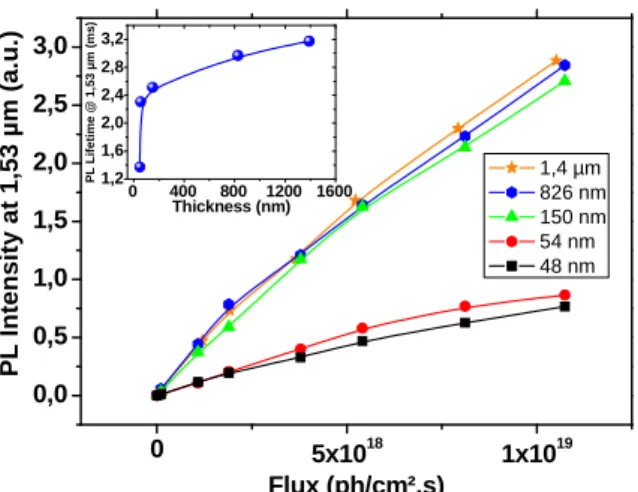
It appears that, whatever is the deposition temperature, the thick samples are approximately 4 times more emitting than the thin samples, after annealing at 900 °C. We re-mind the reader that this annealing is usually used for ap-plications relating to optically excited thick layers or elec-trically excited thin layers [14, 16, 24]. To shed some light on the origin of this difference between thin and thick lay-ers, we performed a more careful study of the effects of the thickness for samples processed with optimized conditions for maximum Er PL (500 °C-deposition, 900 °C annealing). Figure 5 displays the normalized PL intensities of samples with thickness ranging from 48 nm to ~1.4 µm according to the photon flux.
Figure 5 Normalised PL Intensity at 1.53 µm wavelength versus
photon flux for 500 °C deposition annealed 900°C. Inset: Corre-sponding lifetime values.
We can see that, all along the photon flux, the PL intensity for the thin films is significantly lower than that for the thicker ones. A gap even exists when the thickness is creased from about 50 nm to 150 nm, increasing the PL in-tensity by a factor of 4. The PL remains unchanged when the thickness is further increased from 150 nm to about 1.4 µm. An abrupt change was also observed for the evolution of the lifetime, displayed in the inset, showing a steep in-crease from 1.3 ms to more than 2.6 ms when the thickness reaches 150 nm. Such a behaviour of the lifetime towards the thickness, for an unchanged amount of Si excess and Er content can be explained by the evolution of the Local Density of Optical States (LDOS) which increases with the proximity of the substrate, giving rise to a concomitant re-duction of the lifetime [25]. The lifetime improves more smoothly for thicker samples, reaching a value of 3.2 ms at 1.4 µm.
4 Discussion The data reported in Table 1 deserve some comments. First, the quasi linear evolution of the thickness with the deposition duration is largely expected, as being merely due to the constancy of the growth rate. This growth rate appears however slightly lower for the deposition at 500 °C, due to some increasing
interac-tions/reactions between the deposited species, resulting in the formation of volatile elements such as SiO for Td ≥
300 °C [26-28]. Such processes could be, therefore, re-sponsible of the small inflexion of both growth rate and amount of Si excess (Table 1), for the sample grown at 500 °C when compared to that deposited at RT. Apart from this small difference of about 1 at %, the total Si ex-cess determined by XPS appears unchanged with the dura-tion for either RT or 500 °C deposidura-tion. By comparison, the amount of Si excess determined by FTIR is signifi-cantly lower for each temperature deposition and it shows, additionally, a systematic decrease with the deposition du-ration. We have already mentioned that the FTIR approach is unable to detect the Si atoms agglomerating in the form of Si-ncs. The increasing discrepancy between the XPS and FTIR values can be easily explained by the increasing formation of Si-nc when the duration of the deposition is prolonged. This effect is more pronounced for the tion at 500 °C, with the same evolution than a RT deposi-tion, as illustrated by the variation of the fraction of pure Si within Si-ncs, in function of the thickness (Fig. 2). It is clear that the increase of the deposition temperature from RT to 500 °C is expected to favor the formation of Si-nc, through the increasing surface mobility of the sticking elements. For a given thermal budget, the formation of Si-nc is also favored by the thickness iSi-ncrease. In this regards, two corroborating origins have been demonstrated earlier for the thickness dependence of Si-nc formation: (i) the ex-istence of a nucleation barrier for Si-nc in function of the separation distance from the substrate, i.e. the thickness [18,29], (ii) the stress-induced effect which affects the phase separation and then the formation of Si-nc. [19] Concerning the PL properties, consistent results were ob-tained, as shown by the typical spectra of Fig. 3 for the thicker sample deposited at RT. These results allow one to infer that:
- the detection of PL from the as-deposited is indicative of the formation of Si-nc, even at RT, compatible with the ~5% of pure Si estimated for this sample ( Fig. 2). To note that higher emission was detected from the counterpart layer grown at 500 °C (not shown)
- the Er PL is improved with annealing up to the optimum temperature of 900 °C, whereas the visible emission at about 750 nm, usually assigned to Si-nc, collapses after in-creasing the annealing temperature from 600 to 900 °C. This indicates that, in this range of annealing, we are deal-ing with an increasdeal-ing sensitizdeal-ing role of Si-nc which are more coupled to Er ions and then less emitters in the visi-ble. The effects of the thickness is also evidenced by the comparison of the spectra (normalized to the thickness) displayed in Fig. 4 for typical thin and thick sample an-nealed at the optimum 900 °C. It appears that, for both de-position temperatures, the Er emission from the thicker samples is nearly 4 times higher than the thinner ones. This supports the earlier mentioned suggestions concerning the favoring character of the thickness increase for the forma-tion of Si-nc. The benefit of thickness increase is slightly accentuated when the deposition is performed at higher temperature (500 °C). From the evolution of the Er PL
in-0 5x10¹⁸ 1x10¹⁹ 0,0 0,5 1,0 1,5 2,0 2,5 3,0 0 400 800 1200 1600 1,2 1,6 2,0 2,4 2,8 3,2 P L L if e ti me @ 1, 53 µm (m s) Thickness (nm) PL Intensity at 1,53 µm (a.u.) Flux (ph/cm².s) 1,4 µm 826 nm 150 nm 54 nm 48 nm
Phys. Status Solidi C 8,
w
0,00E+000 5,00E+018 1,00E+019
0,0 0,5 1,0 1,5 2,0 2,5 PL Intensity at 1,53 µm Flux (ph/cm².s) 1.33 W/cm² 1.63 W/cm² 1.93 W/cm² 2.22 W/cm²
tensity vs the photon flux, displayed in Fig. 5 for various thicknesses, one can also notice the existence of kind of threshold for the thickness to favorably allow the forma-tion of Si-nc. For the case of Fig. 5 that concerns the sam-ples deposited at 500 °C and then annealed at 900 °C, this thickness threshold is somewhere between 50 and 150 nm. Note also that the observed lifetime for thinnest film (inset Fig. 5) is twice lower than for thicker films, hence contrib-uting to the half decrease for the Er-PL emission of the thin film. The remaining half part of the four-fold reduction of Er PL should be due to lower Si-nc’s sensitization, as the result of lower formation of sensitizers. For the amount of Si excess present in our sample, the layer should be thicker than the threshold value to allow the formation of a sub-stantial density of Si-nc sensitizers. However, since the thickness of the layer should not exceed some tens of nm for electrically-driven Si light emitting devices [16-17,24], the alternative solution is apparently lying in the variation of the Si excess. We have consequently varied the Si ex-cess in thin films (~50nm) deposited at 500 °C and an-nealed at 900 °C, by increasing the power applied on Si cathode. The evolutions of their Er PL intensities vs the flux are shown in Fig. 6.
Figure 6 PL Intensity versus photon flux for different power
ap-plied on the Si cathode, deposited at 500 °C. The reference sam-ple is the ‘1,63 W/cm²’.
It can be seen that the increase of the Si excess leads to a significant improvement of the Er PL to a level compared to that observed for thick samples. Besides, the Er lifetime is continuously decreasing from ~1.8 ms to ~1 ms. This in-dicates that more and more sensitizers are formed in the thin films. The key solution consists, therefore, in more en-richment with Si, which offers the double advantage of minimising the limiting factors related to the film thinness, and favouring the transport of the electrically injected car-riers.
5 Conclusions In summary, the influence of the layer thickness on the formation of Si nanocluster sensitizers have been investigated for two typical deposition
tempera-tures, ambient and 500 °C. It was found that the formation of such Si-ncs is highly thickness dependent, requiring ei-ther layers thicker than a threshold value or more Si excess. The thinness-induced limitations may consist in some bar-rier for the nucleation and growth of Si-ncs, as well as stress-induced effects affecting the phase separation. For the films as thin as tens of nm required for the electrical excitation approach and applications, the alternative was found in more incorporation of Si excess which seems to minimize the thinness-related limiting factors.
References
[1] L. Dal Negro, P. M. Fauchet, and F. Iacona, in: Frontiers in Silicon-Based Photonics – Proceedings of Symposium C of E-MRS, 26–29 May 2008, Strasbourg, France (Physica E 41, 2009).
[2] B. Jalali and S. Fathpour, J. Lightwave Technol. 24, 4600 (2006).
[3] M. Paniccia and S. Koehl, IEEE Spectrum 42, 38 (2005). [4] A. J. Kenyon, P. F. Trwoga, M. Federighi, and C. W. Pitt, J.
Phys.: Condens. Matter 6, L319 (1994).
[5] M. Fujii, M. Yoshida, Y. Kanzawa, S. Hayashi, and K. Ya-mamoto, Appl. Phys. Lett. 71, 1198 (1997).
[6] G. Franzò, V. Vinciguerra, and F. Priolo, Appl. Phys.A, Ma-ter. Sci. Process 3, 69 (1999).
[7] D. Pacifici, G. Franzò, F. Priolo, F. Iacona, and L. Dal Negro, Phys. Rev. B 67, 245301 (2003).
[8] F. Gourbilleau, M. Levalois, C. Dufour, J. Vicens, and R. Rizk, J. Appl. Phys. 95, 3717 (2004).
[9] J. H. Jhe, J. H. Shin, K. J. Kim, and D. W. Moon, Appl. Phys. Lett. 82, 4489 (2003).
[10] F. Gourbilleau, R. Madelon, C. Dufour, and R. Rizk, Opt. Mater. 27, 868 (2005).
[11] M. Wojdak, M. Klik, M. Forcales, O. B. Gusev, T. Gregor-kiewicz, D. Pacifici, G. Franzò, F. Priolo, and F. Iacona, Phys. Rev. B 69, 233315 (2004).
[12] B. Garrido, C. García, S.-Y. Seo, P. Pellegrino, D. Navarro-Urrios, N. Daldosso, L. Pavesi, F. Gourbilleau, and R. Rizk, Phys. Rev. B 76(24), 245308 (2007).
[13] K. Hijazi, R. Rizk, J. Cardin, L. Khomenkova, and F. Gourbilleau, J. Appl. Phys. 106, 024311 (2009).
[14] N. Daldosso, D. Navarro-Urrios, M. Melchiorri, C. García, P. Pellegrino, B. Garrido, C. Sada, G. Battaglin, F. Gourbil-leau, R. Rizk, and L. Pavesi, IEEE J. Sel. Top. Quantum Electron. 12, 1607 (2006).
[15] F. Priolo, C. D. Presti, G. Franzò, A. Irrera, I. Crupi, F. Ia-cona, G. Di Stefano, A. Piana, D. Sanfilippo, and P. G. Fal-lica, Phys. Rev. B 73, 113302 (2006).
[16] O. Jambois, Y. Berencen, K. Hijazi, M. Wojdak, A. J. Ke-nyon, F. Gourbilleau, R. Rizk, and B. Garrido, J. Appl. Phys. 106(6), 063526 (2009).
[17] C. A. Barrios and M. Lipson, Opt. Express 13, 10092, (2005).
[18] Y. C. Fang, W. Q. Li, L. J. Qi, L. Y. Li, Y. Y. Zhao, Z. J. Zhang, and M. Lu, Nanotechnology 15, 494 (2004). [19] I. Ahmad, M. P. Temple, A. Kallis, M. Wojdak, C. J. Oton,
D. Barbier, H. Saleh, A. J. Kenyon,and W. H. Loh, J. Appl. Phys. 104, 123108 (2008).
[21] P. G. Pai, S. S. Chao, Y. Takagi, and G. Lucovsky, J. Vac. Sci. Technol. A 4, 689 (1986); N. Tomozeiu, Appl. Surf. Sci.
25, 376 (2006).
[22] B. J. Hinds, F. Wang, D. M. Wolfe, C. L. Hinkle, and G. Lu-covsky, J. Non-Cryst. Solids 227-230, 507 (1998).
[23] S. Cueff, C. Labbé, J. Cardin, and R. Rizk, IOP Conf. Ser., Mater. Sci. Eng. 6, 012021 (2009).
[24] O. Jambois, F. Gourbilleau, A. J. Kenyon, J. Montserrat, R. Rizk, and B.Garrido, Opt. Express 18, 2230 (2010).
[25] P. Horak, W. Loh, and A. J. Kenyon, Opt. Express 17, 906 (2009).
[26] P. Wickboldt, H. M. Cheong, D. Pang, J. H. Chen, and W. Paul, Mater. Res. Soc. Symp. Proc. 358, 127 (1995). [27] Y. Takakuwa, M. Nihei, and N. Miyamoto, Jpn. J. Appl.
Phys. 32(2), L480 (1993).
[28] D. Gautam, E. Koyanagi, and T. Uchino, J. Appl. Phys. 105, 073517 (2009).
[29] M. Zacharias and P. Streitenberger, Phys. Rev. 62, 8391 (2000).