Biasing Techniques for Linear Power Amplifiers
by
Anh Pham
Bachelor of Science in Electrical Engineering and Economics California Institute of Technology, June 2000
Submitted to the Department of Electrical Engineering and Computer Science in partial fulfillment of the requirements for the degree of
Master of Engineering in Electrical Engineering and Computer Science at the
MASSACHUSETTS INSTITUTE OF TECHNOLOGY May 2002
@ Massachusetts Institute of Technology 2002. All right reserved.
8ARKER &UASCHUSMrS Wi#DTE OF TECHNOLOGY
JUL 3 12002
LIBRARIES AuthorDepartment of Electrical Engineering and Computer Science May 2002
Certified by _
Professor of Electrical Engineering and
Charles G. Sodini Computer Science Thesis Supervisor
Accepted by
Arthuf-r ESmith, Ph.D. Chairman, Committee on Graduate Students
Biasing Techniques for Linear Power Amplifiers
by
Anh Pham
Submitted to the Department of electrical Engineering and Computer Science on May 10, 2002 in partial fulfillment of the requirements for the degree of Master of Science in Electrical
Engineering and Computer Science
Abstract
Power amplifiers with conventional fixed biasing attain their best efficiency when operate at the maximum output power. For lower output level, these amplifiers are very inefficient. This is the major shortcoming in recent wireless applications with an adaptive power design; where the desired output power is a function of the bit-error rate, channel characteristics, modulation schemes, etc. Such applications require the power amplifier to have an optimum performance not only at the peak output level, but also across the adaptive power range.
An adaptive biasing topology is proposed and implemented in the design of a power amplifier intended for use in the WiGLAN (Wireless Gigabits per second Local Area Network) project. Conceptually, the adaptive biasing circuitry senses the input signal, scales appropriately, then takes the average. The result dc signal is used to moderate the biasing current for the power transistors. The bias level is; therefore, a function of the input signal. By selecting the
appropriate scaling factor, the biasing current can be adjusted to improve the efficiency across a wide range of operating power levels.
The power amplifier that was designed, has two stages with a nominal gain of 17.3dB. The output at 1 -dB compression point is 20dBm. Both stages employ the adaptive biasing technique. The peak efficiency is 35% at l9dBm output power while the mid-range operation efficiency
shows a significant improvement from conventional fixed biasing. Operating at 5.8GHz center frequency, the amplifier also exhibits good linearity with -56.66dBc and -58.1 ldBc, 2n and 3rd
Acknowledgements
The work presented in this thesis could not have happened without the help and support of many people. First, I would like to thank Professor Charles Sodini for providing me with this research opportunity. His guidance is instrumental and his intuition approach to technical problems is intriguing. I am also greatly indebted to all of my colleagues in the H. S. Lee and C. G. Sodini research groups. Don Hitko vast knowledge and experience in circuit design are essential to the completion of this thesis work. Todd Sepke is always patient and helpful with design tools and
other computing issues. I found solutions for a lot of the problems during our countless coffee break discussions. I would like to thank Andy Wang for his help on system issues that I often ran into during the course of this thesis. Andrew Chen and Mark Peng seem to know all the
tricks to get things done around MIT, and are willing to offer their assistance. Andrew is the photographer for all the photos presented in this thesis. I greatly appreciate all the groups'
members for making our office a friendly and supportive research environment.
I would like to express my gratitude to Jeff Gross, and Eric Johnson at IBM for their support on the SiGe process. Aiman Shabra, a former colleague, and Bob Broughton at ADI offered tremendous help with packaging. I am grateful for their kind support.
Vickram Vathulya at Philips Research USA introduced me to integrated power amplifier design and shared his industry "how-to" experience many times thereafter. I would like to thank Philips Research USA, especially Satyen Mukherjee and Tirdad Sowlati, for giving me the opportunity to design power amplifiers for GSM and CDMA cellular phones.
Marilyn Pierce helps me greatly with all the deadlines and administrative requirements that I often overlook. I greatly appreciate her dedication.
I would like to thank Pat Varley, and her successor Kathy Patenaud, for their help with all the purchasing and paperwork.
I would like to thank my parents for their support and encouragement. Their love for me is simply boundless.
Contents
I
Introduction ... 131.1 Pow er Am plifier Biasing ... 14
1.2 Efficiency... 14
1.3 Fully Integrated Pow er Am plifier Issues ... 16
1.4 The W iG LAN Project ... 16
1.5 Thesis Overview ... 16
2 N onlinearities and Pow er Link B udget ... 19
2.1 D istortion ... 19
2.1.1 H arm onics ... 20
2.1.2 1-dB Com pression ... 21
2.1.3 IIP3 and Interm odulation Products ... 21
2.2 Receiver Sensitivity and Bit-Error-Rate (BER)... 23
2.3 Path Loss... 25
2.4 Pow er Link Budget ... 26
3 C onducting Pow er A m plifiers ... 29
3.1 Class-A ... 30
3.2 Reduced Conduction Angle Mode, Class-AB, B and C ... 32
4 B iasing T echniques... 39
4.1 Current M irror N etw ork... 39
4.1.1 H ow does it w ork? ... ... ... ... . . 40
4.1.2 Effects on gain, linearity, and efficiency ... 41
4.2 D iode-Connect ... 43
4.2.1 H ow does it w ork? ... ... ... 43
4.2.2 Effects on gain, linearity, and efficiency ... 43
4.3 Cascode Current M irror ... 45
4.3.1 H ow does it w ork? ... ... ... ... . . 45
4.3.2 Effects on gain, linearity, and efficiency ... 46
4.4 A daptive Biasing... 47
4.4.1 The Concept ... 47
4.4.2 H ow does it w ork? ... ... ... 48
5 D esigning a C lass-A Pow er A m plifier ... 55
5.1 Optim al Load and Output M atching N etw ork ... 55
5.1.1 Conjugate M atch vs. Pow er M atch... 55
5.1.2 Optim al Load ... 56
5.1.3 M atching N etw orks... 58
5.2 Transistor Size and Biasing Point... 68
5.3 G ain and M ultiple Stages... 69
6 Power Amplifier Design Example for WiGLAN ... 73
6.1 Specification ... 73
6.2 Determine ROp1 . . . . 73
6.3 Output M atching N etw ork ... 74
6.4 Output Stage Transistor Size ... 76
6.5 Output Stage G ain and Im pedance ... 76
6.6 Output Stage Biasing ... 79
6.6.1 Fixed Biasing Topologies ... 79
6.6.2 A daptive Biasing Topology ... 79
6.7 Driver Stage ... 80
7 Sim ulation R esults ... 81
7.1 Gain, Efficiency, and Linearity Perform ance ... 81
7.2 Layout ... 83
8 M easurem ent Procedure and R esults ... 85
8.1 Die Photo and Packaging ... 85
8.2 Test Board... 86
8.3 M easurem ent Setup... 86
8.4 Results... 87
9 C onclusion ... 91
Appendix A . H arm onics C alculation ... 93
Appendix B. Gain and Input Impedance Calculation... 96
Appendix C. Schem atics ... 98
List of Figures
Figure 1-1: Basic Pow er Am plifier Circuit... 14
Figure 1-2: Collector Voltage and Current Waveforms ... 15
Figure 1-3: Typical Power Amplifier Efficiency Curve ... 15
Figure 2-1: Pow er A m plifier M odel ... 19
Figure 2-2: 1-dB Com pression Point ... 21
Figure 2-3: Two-Tone Test Output Spectral Density ... 22
Figure 2-4: Input Third Intercept Point... 23
Figure 2-5: BER Curves for Gaussian and Rayleigh Channels ... 25
Figure 2-6: Transceiver Block Diagram for Power Link Budget ... 26
Figure 3-1: A 2-Port Model of An Inductively Coupled Power Amplifier ... 29
Figure 3-2: Equivalent Power Amplifier Models for (a) Conducting Classes and (b) Switching C la sse s... 3 0 Figure 3-3: Waveforms of A Class-A Power Amplifier... 31
Figure 3-4: Power Amplifier Circuits for Calculating Output Power and DC Power... 31
Figure 3-5: Waveforms of A Reduced Conduction Angle Amplifier... 32
Figure 3-6: Efficiency and Maximum Output Power (Normalized to Class-A) vs. Conduction A n g le ... 3 6 Figure 3-7: DC and Harmonics Components of The Output Current... 37
Figure 4-1: Current M irror B iasing... 39
Figure 4-2: Base-Em itter V oltage Loop ... 40
Figure 4-3: Small Signal Equivalent Circuit for Conventional Biasing ... 41
Figure 4-4: D iode-Connect Biasing ... 43
Figure 4-5: Small Signal Equivalent Circuit for Diode-Connect Biasing ... 44
Figure 4-6: Cascode Current Mirror Biasing ... 45
Figure 4-7: Small Signal Equivalent Circuit for Cascode Current Mirror Biasing ... 47
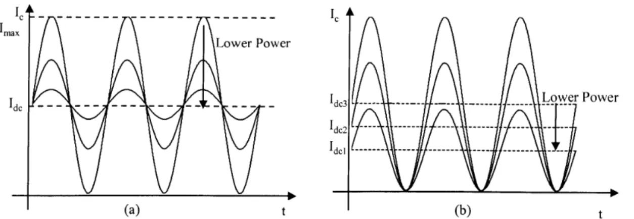
Figure 4-8: Collect Current in Fixed Biasing (a) and Adaptive Biasing (b)... 48
Figure 4-9: Adaptive Biasing Circuit Concept ... 48
Figure 4-10: A daptive B iasing... 49
Figure 4-11: Small Signal Equivalent Circuit for Adaptive Biasing ... 51
Figure 4-12: R -C A veraging Circuit ... 51
Figure 4-13: Ripple Attenuation of the Averaging Circuit with Different Pole Location... 52
Figure 4-14: Example of 256-QAM Waveform with Symbol Period Ts, Carrier Period Tc, and A veraging T im e C onstant ... 53
Figure 5-1: Current Generator with Impedance Zs Delivers Power to Load ZL ... 55
Figure 5-2: Conjugate Match Yields Less Power than Power Match... 56
Figure 5-3: Power Amplifier Optimal Load ... 57
Figure 5-4: Maximum Linear Collector Current and Voltage Waveforms ... 57
Figure 5-8: Mismatched Circles vs. Power Contours ... 62
Figure 5-9: Im pedance M atching... 63
Figure 5-10: L-C M atching Section... 63
Figure 5-11: L-C M atching Using Sm ith Chart... 64
Figure 5-12: Frequency Response of an L-C Matching Section for Different m Ratios... 65
Figure 5-13: Single and Double L-C Matching Sections Bandwidths ... 66
Figure 5-14: Replacing Parallel Capacitors with Equivalent Harmonics Shorts... 67
Figure 5-15: B JT fT C urve... .... 69
Figure 5-16: Two-Stage Pow er Am plifier ... 70
Figure 5-17: Gain Partitioning in M ultiple Stages... 70
Figure 6-1: 2-Section L-C Low-Pass Matching Network... 74
Figure 6-2: Output Matching Network with Packaging Parasitic Inductor ... 76
Figure 6-3: Equivalent Small Signal Model with Emitter Wire-Bond Inductor... 77
Figure 6-4: Gain and Input Impedance vs. Emitter Degeneration ... 78
Figure 6-5: Replacing the Conventional Biasing Resistor with the Adaptive-Current PMOS in the A dapting B iasing Schem e... 79
Figure 7-1: Gain vs. Output Power Curves for PAs with Four Different Biasing Topologies.... 81
Figure 7-2: Power Added Efficiency Curves vs. Output Power... 82
Figure 7-3: Output Spectral Density (normalized to the carrier) at Maximum Output Power .... 82
Figure 7-4: Phase Variation across the Output Power Range... 83
Figure 7-5: Adaptive Biasing Power Amplifier Layout ... 84
Figure 8-1: Pow er A m plifier D ie Photo... 85
Figure 8-2: T est B oard Photos ... 86
Figure 8-3: M easurem ent Setup... 86
Figure 8-4: Negative Feedback to Reduce Gain and Stop Oscillation ... 87
Figure 8-5: Measurement Results for Power Amplifier with R-C Feedback ... 88
Figure 8-6: Second Assembled PA without Feedback Measurement Results... 89
Figure B-1: Small Signal Model for Output Stage Gain and Impedance Calculation... 96
Figure C-1: Schematics for Conventional Biasing Power Amplifier ... 98
Figure C-2: Schematics for Diode-Connect Biasing Power Amplifier ... 100
Figure C-3: Schematics for Cascode Current Mirror Biasing Power Amplifier ... 102
List of Tables
Table 2-1: Power Amplifier Output in Response to a Single Tone Input... 20
Table 2-2: Power Amplifier Output in Response to a Two-Tone Input ... 22
Table 2-3: Example Values for Receiver Sensitivity... 25
Table 2-4: Path Losses at Various Distances for Typical Wireless Standards ... 26
Table 2-5: Typical Required Transmitting Power for the WiGLAN PA in Rayleigh Channel... 27
Table 3-1: M odes of O peration... 33
Table 3-2: DC and Harmonics Components of Output Currents in Reduced Conduction Angle O p eration M od es... 37
Table 6-1: WiGLAN Power Amplifier Specification... 73
Table 6-2: Device Parameter for NPN transistor, SiGe 6HP... 77
Table C-1: Component Values - Conventional Biasing Power Amplifier... 99
Table C-2: Component Values - Diode-Connect Biasing Power Amplifier ... 101
Table C-3: Component Values - Cascode Current Mirror Biasing Power Amplifier... 103
1
Introduction
Because of the explosion of wireless PDAs (Personal Digital Assistant) use, we are now living in a "mobile" information era where information from every corner of the world is available at the touch of a fingertip regardless of our location. However, current wireless systems are too costly
and limited to exploit this vast amount of information. What we need is not merely a wireless connection, but a fast, efficient, and reliable wireless connection.
Every wireless system employs one or multiple power amplifiers, and it is usually the case that the performance of a wireless system is determined by the linearity and efficiency of its power amplifiers. However, current linear power amplifiers are very inefficient. They are the most power "hungry" block in a wireless system, and they consume many times the combined power
of the rest of the transceiver circuitry. Not only do they severely reduce the battery lifetime, but they also degrade the performance of adjacent circuitries by releasing tremendous amounts of heat. The need for an efficient linear power amplifier has been the focus of much industrial and academic research in the past decade.
Moreover, although power amplifiers have been used since the early days of transistors, there is no comprehensive documentation of its biasing techniques. Thorough knowledge of various biasing topologies and the tradeoff between them will greatly help power amplifier designers. Motivated by the above challenges, this thesis focuses on high efficiency biasing techniques for power amplifiers. Three power amplifiers, each uses a different biasing topology, are designed
and simulated to study and compare the three biasing circuits. In addition, an innovative adaptive biasing topology is proposed. An adaptive biasing power amplifier is designed, fabricated, and tested to demonstrate the proposed concept.
The remainder of this chapter presents an overview of the thesis. We will begin by reviewing specific issues in biasing, efficiency, and SOC (System On Chip) that often challenge power amplifier designers. As the thesis is part of the ambitious WiGLAN project, a brief introduction of the WiGLAN is presented to explain the challenges and requirements for the power amplifier design. The chapter concludes with a detailed outline of the thesis.
1.1 Power Amplifier Biasing
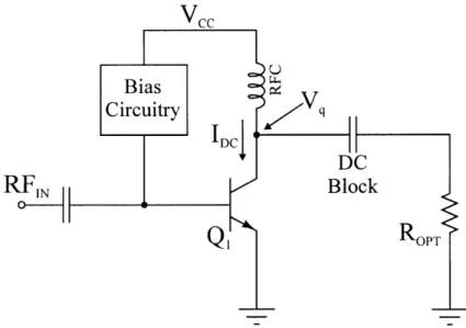
Antenna Bias Circuitry |Output Matching DC Block RFin Power Transistor Q,Figure 1-1: Basic Power Amplifier Circuit
Figure 1-1 shows a basic power amplifier circuit with the power transistor connected to the supply via an RF choke (RFC). The output matching circuit transforms the output impedance to the 50Q antenna load. The goal is to provide the bias circuitry for the power transistor. Much of the amplifier operating conditions and performance depend largely on this biasing circuit.
The collector current of a power transistor is usually in the range of hundreds of milliamps. Therefore, any emitter degeneration resistor is undesirable*. The use of the RF choke allows the collector to connect directly to the supply voltage with minimal loss. In order to achieve high
efficiency, the biasing circuitry should consume as little power as possible. Also, its impedance
should be large so that it does not load the RF circuit and reduce the gain.
1.2 Efficiency
Assume transistor Qi in Figure 1-1 is biased with a fixed quiescent current I, and voltage V,. The set (V; , Iq) is usually called the transistor's biasing point. When an RF input is applied, the
collector current and voltage swing around their respective biasing points. Figure 1-2 shows an example of the collector current and voltage waveforms under sinusoidal excitation.
Smaller power Vnmsiax
..--- -.. -....-
-.. --- -..
...
I' Smaller power InmsImax
----
---t
t
Figure 1-2: Collector Voltage and Current Waveforms
Let 1,.Im, and V,§ be the largest root mean square value for the collector current and
voltage, respectively. Assume a lossless matching network, the maximum rms (root mean square) output power is given by
Pmax = rmsmaxIrmsjmax (1-1)
Under the bias condition of V and I, the supply power is
Pd, = VqIq (1-2)
Therefore, the maximum attainable efficiency is
77=max - r;msImax 'rms~max
P VI
dc q q
Depending on the current and voltage waveforms as well as efficiency could be anywhere from 0 to a theoretically ideal
PAE
inlax
P
P.-their relative phases, the maximum value of 100 percent.
Figure 1-3: Typical Power Amplifier Efficiency Curve
V,
V-(1-3)
When a smaller input is applied, the voltage and current swings are smaller, and the output power is smaller than P..a However, since the bias points Vk, and Iq are fixed, the supply
power stays constant regardless of the input. Therefore, the power amplifier efficiency drops at lower output levels. Figure 1-3 shows a typical PAE (Power Added Efficiency) versus output power curve. The power amplifier is most efficient when operating at its maximum designed output power.
Power amplifiers with this type of efficiency curves work fine for fixed output power
applications. However, they pose a significant shortcoming for adaptive power systems, where the output power varies depending on the channel condition.
1.3 Fully Integrated Power Amplifier Issues
With the advanced development of semiconductor and integrated circuit technologies, system on chip (SOC) is now the favored possibility. However, power amplifiers remain a sticky issue for integrated circuit systems. Designers face two main challenges for fully integrated power amplifiers. First, as the technology scales, both supply voltages and transistor breakdown voltages become smaller. For the same output power, the current increases as the voltage decreases. Designers now have to work with much higher currents that make them more vulnerable to parasitic and series resistor loss. Second, spiral on-chip inductors are too lossy for matching networks, especially output matching networks where RF power is high.
Overcoming these challenges will require much more research and innovations.
1.4 The WiGLAN Project
The power amplifier designed in this thesis is intended for use in the ongoing WiGLAN (Wireless Gigabit per Second Local Area Network) project in the Microsystems Technology Laboratory (MTL) at MIT. Using the ISM (Industry Scientific and Medical) band at 5.8GHz with 150MHz bandwidth, the project calls for a design of a wireless network with 1 Gigabit per
second throughput. In order to achieve such a high speed, an adaptive modulation scheme utilizing multiple OFDM (Orthogonal Frequency Division Modulation) channels with up to
256-QAM (Quadrature Amplitude Modulation) is used. Such a modulation scheme requires a power amplifier with extremely high linearity.
Moreover, in order to maximize battery lifetime, the WiGLAN also adapts the transmitting power based on the distance to receivers and environment conditions. Power adaptation poses yet another challenge to the power amplifier designs. As discussed earlier, conventional power amplifiers are very inefficient at lower output levels. Therefore, innovative biasing techniques are required to improve low level operation efficiency.
1.5 Thesis Overview
The rest of the thesis is divided into two parts. The first part, Chapter 2-5, provides relevant background and detailed theoretical analysis for power amplifiers. Chapter 2 reviews useful RF terminologies and nonlinearities. Chapter 3 discusses the conducting power amplifier modes,
Class-A, AB, B, and C. Detailed operation of each mode is studied to determine the tradeoff between gain, efficiency, and linearity. In Chapter 4, three fixed power amplifier biasing topologies as well as the proposed adaptive biasing technique are presented. For each topology, details of the bias setting mechanism, as well as effects on gain, linearity and efficiency of the overall amplifying stage are discussed and compared. Chapter 5 goes over the step-by-step design of a class-A power amplifier. Extra efforts are given to demonstrate and clarify the difference between power match and conjugate match in power amplifier design.
The second part of the thesis, Chapter 6-9, is devoted to the practical designs of power amplifiers to validate the observation of the four biasing topologies studied in Chapter 4. In Chapter 6, a 5.8GHz, 20dBm class-A power amplifier is designed using the step-by-step procedure from Chapter 5. The power amplifier has four versions, each using one of the four biasing techniques discussed in Chapter 4. Simulation results of the design are presented and discussed in Chapter
7.
The adaptive biasing version of the power amplifier is fabricated in the IBM SiGe 6HP BiCMOS process. Chapter 8 explains the fabrication, test board, and measurement setups for the power
amplifier. Measurement results are provided in Chapter 9. Chapter 10 concludes the thesis and discusses further research topics on the subject.
2 Nonlinearities and Power Link Budget
This chapter reviews some general nonlinearity and RF terminologies. Most of these
terminologies, in general, apply for all gain blocks. For simplicity, however, they are addressed here in the context of a power amplifier.
Power amplifiers are usually designed for a certain set of specifications such as output power, efficiency, and linearity. However, power amplifier designers often have to design their PA to work with a certain given set of receiver characteristics and channel link to produce a certain required bit-error-rate output. In such cases, designers have to start from the receiver output, work their way back through the receiver chain and the channel link to derive the acceptable
specifications for the power amplifier. Therefore, familiarity with receiver characterizations as well as the channel link is certainly helpful for power amplifier designers. The last part of this chapter addresses this connection and suggests a rough estimation for the power link budget of a transceiver.
2.1 Distortion
xOt
P>
y (t)
PA
Figure 2-1: Power Amplifier Model
Power amplifiers are usually nonlinear, which results in unintended signals with frequencies outside of the band of operation. These out-of-band signals can cause significant interference to other channels. In order to study the nonlinearity, we use a polynomial series to model the power amplifier as suggested by Razavi [1]. For simplicity, we restrict our analysis to fifth order
Let y()=a1x(t)+a2x(t) +a3x( 3 +a3x( 4 +a5x(tY be the output when an input x(t) is applied to the power amplifier as shown in Figure 2-1.
2.1.1 Harmonics
If a sinusoidal x(t)= A cos(ot) is applied to the power amplifier, then the output is given by
y
(t)=
aA cos(ot)+ a2(Acos(ot))
2 +a(A
cos(t))3+a4 (A cos (ct))4 +a5 (A cos (Cot))
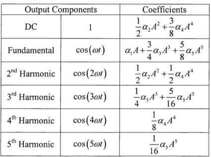
Expanding the high order terms using trigonometric identities, we can rewrite the output in terms of dc, fundamental and harmonic components. Please refer to Appendix A for detail calculation; the result is listed here in Table 2-1. The second column contains the dc, fundamental and harmonic terms. The coefficients for these terms are in the third column.
Table 2-1: Power Amplifier Output in Response to a Single Tone Input
Because of the nonlinear behavior, the output contains integer multiples of the input frequency. These higher frequency components are called harmonics. To minimize interference to other bands, these harmonics components should be suppressed as much as possible. FCC (Federal Communications Commission) Part 15 specifies the rules regarding harmonics signals of a transmitting system.
Output Components Coefficients
1 3 4
DC 1 -a 2A2 +-a4A4
2 8
35
Fundamental cos(ct) aA+-aA3 +-,A 5
4 8
2nd Harmonic cos(2cot) a2A2 +-aA 4
2 2
3rd Harmonic cos(3wt) 1a3A + 55
4 16
4th Harmonic Cos(4cot) -a4A 4
8
5th Harmonic Cos(5ct) I a5A5
2.1.2
1-dB Compression
POUT
.. ... dB.
1
P1-dB PIN Figure 2-2: 1-dB Compression Point
From Table 2-1, the above amplifier has a fundamental gain of a, A +-a 3A3 +-5aA , where A
4 8
is the input amplitude. In low power operation, where A is small, aA is much larger than 35
- a3A3 + -a 5A. In this case, the fundamental gain is approximately a1A. On the
logarithmic-4 8
scale plot, the output power versus input power curve has a slope of 1 at low power levels.
3
3+5 5As A increases, -ca3A3 +- k 5A increases faster than a,A. Therefore, as the input power rises
to a certain level, 31a
3A~ ± -5a5A5 is no longer negligible compare to ajA. If a3 and a5 are
4 8
negative, the gain starts leveling off when A is sufficiently large. In other words, the gain is "compressed" from its extrapolated linear value. The 1-dB compression point is defined as the input power level where the gain drops by 1 -dB as shown in Figure 2-2.
An important observation from the fundamental term coefficient is that only the odd power terms in the polynomial series (Ca3 and aC in this case) affect the fundamental gain.
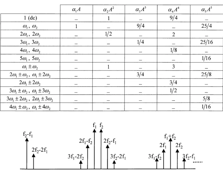
2.1.3 IP 3 and Intermodulation Products
When a signal with two different frequency components x (t) = A, cos (cot) + A2 cos (co2t) is
applied to the power amplifier, the output exhibits multiple mixings of the two frequencies called intermodulation products (IM). Using the same power amplifier model,
y (t)= a,
(A,
cos(ot)+
A2 cos (o2t)) + a2(A,
cos (Coit)+ A2 cos(C2t))2+a3 (A1 cos
(Colt)+
A2 cos ((02t + a4 (A cos(ot)+
A2 cos (0 2t)) 4+a5 (A1cos (~0t)+ A2cos (C 2t )
5
(2-2)
For simplicity, we assume here that the two tones have the same amplitude, i.e. A, = A2 = A. Expanding the series, besides the familiar dc, fundamental and high-order harmonics
components with frequencies co,, 2a1, 3to, 4a1, 5col, co2, 2CO2, 3tO2 , 402, and 502, we also have intermodulation components between the two input frequencies. Again, detailed
calculation is presented in Appendix A. The result is listed here in Table 2-2. The first column represents the output frequency components. The top row shows represents the amplitude. The
grid contains the respective coefficients. A "-" represents a zero.
Table 2-2: Power Amplifier Output in Response to a Two-Tone Input
1
(dc) _1
_ 9/4 _ Col, C2 1 _ 9/4 - 25/4 2co, 2o2 - 1/2 - 2 -3co, 302 - - 1/4 - 25/16 4co, 42 - _ _ 1/8 -5 co, , 5 2 - - 1/16 (0+( t) 1 -3
-2o +-2o, ± 2+ 2 -_ 3/4 - 25/8 2(01 2c2 - - - 3/4-3co±2 co, (±3co2 - _ _ 1/2
-3co, ±2(02, 2o± 32 _ _ - 5/8 4co± co2, 0± 402 _ _ _ _ 1/16 fl f2 f2-fl A 2f2-2f1 2f, -f2 3f -2f2 2f2-f1 3f2-2f1
f,
A 2f, 2f 2 3fH f2 f2-flFigure 2-3: Two-Tone Test Output Spectral Density
a2A 2 a4A 4 aA A5
Of particular interest are the third-order and fifth-order IMs with frequencies (2co, - (02), (202 - Cl), (3co, -2 2), and (3CO2 2co,) because when C, and C2 are close enough, these
third-order and fifth-order products could fall in the band of interest. The rest of the
intermodulation products are usually further away from the operating band that receiver filters easily suppress them. At low power level when A is small, a3A3 is much larger than a5A'. Therefore, on the logarithmic-scale plot versus the input power, the power of these third-order IMs has a slope of 3 because their amplitudes are proportional to A3. Analogously, the power of the fifth order IMs has a slope of 5 as shown in Figure 2-4.
Power amplifier linearity is usually specified by IIP3 (input third intercept point), which is
defined as the input power where the third-order IM power is as large as the fundamental. POUT Fundamental 3 3rd m 5thIM IP 3 PIN
Figure 2-4: Input Third Intercept Point
2.2
Receiver Sensitivity and Bit-Error-Rate (BER)*
Receiver sensitivity is defined as the minimum signal power at the receiver antenna that can produce an acceptable signal to noise ratio. To calculate the sensitivity, we start with the noise
figure equation
NF = SNRin Prx ant (prs noise *BW (2-3)
SNROL, SNRout
where
P antis the receiving signal power at the antenna,
Pnoise is the source resistance noise power per unit bandwidth, assume conjugate match at the input, P noise = kT = -I74dBm/Hz,
SNRO1 , is the signal to noise ratio at the output of the receiving chain.
Rearrange the terms,
PIXant =NF * SNRou,* Ps -nois *BW (2-4) By definition, P,, , is the receiver sensitivity S0 when SNRou, is smallest. In dB terms,
SO =-l 74dBm/Hz + NFdB +1 logBW+SNR ,,4
in-band -white-noise (2-5)
total-noise-floor
Given a specific communication channel with a certain bandwidth and receiver noise figure, we can use equation (2-5) to calculate the sensitivity from the minimum signal-to-noise ratio. However, the minimum signal-to-noise ratio is often given in terms of bit-error-rate (BER), which is defined as the average number of erroneous bits observed at the output of the receiver divided by the total number of bits received in a unit time.
Let Eb be the bit energy,
R be the data rate (i.e. IGb/s),
N be the white Gaussian noise power spectral density.
Then the total signal power is R * Eb , and the total noise power is B W * N. Therefore,
SNR t = igna R *Eb R (E (2-6)
Pnoise BW*N0 BW
No
Eb
/N
directly relates to the bit-error-rate. Depends on modulation types and coding schemes,we can readily use BER versus Eb /NO curves to determine Eb /NO from a given value of BER. A typical BER versus Eb
/N
plot for a Gaussian and a Rayleigh channel is shown in Figure 2-5. From equation (2-5), replace SNR OUtI with equation (2-6)SO =-74dBm/Hz + N~d +10logR+101og ( (2-7)
in-band -white-noise
Since Eb /NO is determined for a given BER, equation (2-7) allows us to directly calculate the receiver sensitivity based on BER. One interesting observation from the equation is that sensitivity is independent of bandwidth when expressed in terms of Eb /NO .
Table 2-3 shows some example values for receiver sensitivity of typical receiver specifications. The values are calculated for two channel types, Gaussian and Rayleigh channels.
Values for Receiver Sensitivity 101 10 10'1 10-10 10-6 10 -0 5 10 15 20 25 30 35 Eb/No (dB)
Figure 2-5: BER Curves for Gaussian and Rayleigh Channels Courtersy of Andy Wang M.S. Thesis [2]
2.3 Path Loss
Signals propagating through free space experience a power loss proportional to the square of the distance. However, in a typical wireless LAN environment, there are walls, furniture, moving objects, reflecting surfaces, ... For these environments, the exponential proportionality constant is larger than 2, with experimental measurement values for a typical office setting between 3 and
Receiver Sensitivity So
Specification Gaussian Channel Rayleigh Channel
Receiver Noise Figure NFdB = 6dB
Data Rate R=lGbit/s (256-QAM) -71 dBm -54 dBm
Bit-Error-Rate BER=1 03
Receiver Noise Figure NFdB = 6dB
Data Rate R=lMbit/s (4-QAM) -101 dBm -84 dBm
Bit-Error-Rate BER=1
0~3
Table 2-3: Example ... ... . .. ... .. .. ... .... ... .... ...* . .. . . .... ....... .. ...... .. ... ... ... .... ... . .. . . .. . ... ... ... ... ... 7 7 7 7 . . . . . . . . . . . . : : : : : : : : : : : : : : : : - : . . I *. ' .' * . . . .. . . . . .. * . .. . . . .. .. . . . . . . . . . . . . . . . . . . .. .. . . . . . . . .. .. . . . .. . . . . . . . . . . . . . . . . . . . .. . . . . . . . . . . .. . . .. . . . . . . . . . . . . . . . . . . . . . . .. . . . . . . .. .. .. .. . . . . . . . .. . . .. . . . . . . . . . . . ... . . .. . . . . . . . . . . . . . . . . . . . . . . . . . . . . . . . . :7 7 . . . .. . . . . .. . . . . . . . . .. . . . .. . . . . . . . . . . . . . . . . . . . . . . . .. . . . . . . . . . . ... . . . .Lave = -10 log 2 n (2-8)
with
2 = c/f is the signal wavelength in meter,
d is the distance between transmitter and receiver in meter, n is the path loss exponent.
Table 2-4: Path Losses at Various Distances for Typical Wireless Standards
d =1m d=10m d =100m
Blue Tooth (fo = 2.4 GHz) 29 dB 59 dB 89 dB
802.11a (fo = 5.3 GHz) 36 dB 66 dB 96 dB
WiGLAN (fo = 5.8 GHz) 36.7 dB 66.7 dB 96.7 dB
2.4 Power Link Budget
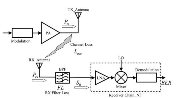
TXAntenna P -- A PA Modulation Channel Loss Lave RXAntenna LO BPF Demodulation: P:X LNA So * BER FL
>:
Mixer RX Filter Loss Receiver Chain, NFFigure 2-6: Transceiver Block Diagram for Power Link Budget
We can use our knowledge of power amplifier and receiver characteristics to plan the power link budget for the WiGLAN. Consider the block diagram for the WiGLAN transceiver as shown in Figure 2-6 where
P, is the transmitter power,
FL is the receiver filter loss, S0 is the receiver sensitivity,
NF is the total noise figure of the receiver chain,
P, = P,+ L, = So + FL+ L,
Replacing the terms on the right from equations (2-7) and (2-8).
P =-174+NF+101ogR+101ogb + No Receiver Sensitivity FL +10log Filter Loss Path Loss
Given the data rate R
,
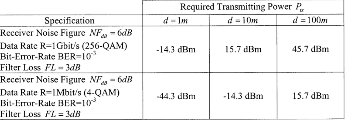
bit error rate (in terms of Eb /NO ), and the distance d, equation (2-10) relates the transmitting power P, to the receiver noise figure NF .Table 2-5: Typical Required Transmitting Power for the WiGLAN PA in Rayleigh Channel
Required Transmitting Power P,
Specification d = lm d =10m d = 100m
Receiver Noise Figure NFdB = 6dB
Data Rate R=IGbit/s (256-QAM) -14.3 dBm 15.7 dBm 45.7 dBm Bit-Error-Rate BER= 10-3
Filter Loss FL =
3dB
Receiver Noise Figure NFB = 6dB
Data Rate R=lMbit/s (4-QAM) -44.3 dBm -14.3 dBm 15.7 dBm Bit-Error-Rate BER=10 3 Filter Loss FL = 3dB (2-9) (2-10) 2 (4;T)d" n
3 Conducting Power Amplifiers
Power amplifiers are divided into classes based on their output waveform shapes and relative phases. However, the actual implication of the power amplifier classes is related to the three
main figure-of-merits: gain, linearity, and efficiency. Before discussing power amplifier classification, we shall first review the definitions for gain, efficiency, and linearity.
PDC
R S
---C
-1H
I1H
--
-- --
I
INPUT
VV
OUTPUT
9VMATCHING IN
MATCHING
R
NETWORK
P
NETWORK LOADFigure 3-1: A 2-Port Model of An Inductively Coupled Power Amplifier
Consider a simple power amplifier as a two-port network in Figure 3-1. The dc supply is connected via an RFC (Radio Frequency Choke). Such a supply configuration is called inductively coupled. Assume that both input and output matching networks are lossless. The power amplifier gain is simply
P
G = ' (3-1)
p Where Pi, is the input power, and
P'u, is the output power.
(3-2)
d7
= e
Where P, is the dc supply.
Usually when the gain is large, P, is much larger than Pj, then efficiency is loosely defined as
')Ut /Pd.
Power amplifier linearity is usually specified by the input third order intercept product IIP3 as
discussed in chapter 2. Intuitively speaking, a power amplifier is perfectly linear if its response to a single frequency input signal contains no other frequency components besides the input frequency. r-_ I
Matching
Network
RLoad C-C= -CI C_-I cam--- - I(a)
RLoad(b)
Figure 3-2: Equivalent Power Amplifier Models for (a) Conducting Classes and (b) Switching Classes
There are two main types of power amplifier classes: the conducting classes and the switching classes as shown in Figure 3-2. In conducting-class power amplifiers, the transistor acts as a current source generator driving a resistive load. Depending on the current waveforms,
conducting-class power amplifiers can be very linear. Switching-class power amplifiers, on the other hand, use the transistor as a switch. They rely on a resonant tank network to store energy and switch the transistor on and off to divert the stored energy to RE output power. Because of the switching nature operation, switching-class power amplifiers are extremely nonlinear and unsuitable for the type of quadrature amplitude modulation employed by the WiGLAN. Therefore, we will limit our discussion here to conducting-class power amplifiers where good
linearity is inherited.
3.1 Class-A
A power amplifier operates in class-A mode when its power transistors are on for the entire period of the input signal. Therefore, a class-A amplifier is said to have a 3600 conduction angle.
Resonant
Tank
Assume there is a base-emitter voltage V,(,,,, above which the transistor is on, and below which
the transistor is off. In order for the amplifier to operate in class-A mode, the transistor has to be
biased with a base voltage Vbia, such that the base voltage V" is larger than Vb() during the
entire period. In such case, the transistor output voltage and current waveforms are pure sinusoidal as shown in Figure 3-3.
vbia N Z2 Input vbe(on) --- - --- -- --- --- voltage -- -Current -v V--- --- utput _________________________________Voltage t
Figure 3-3: Waveforms of A Class-A Power Amplifier
Vcc Bias Circuitry 1Dj Vq DCC
RFIN
BlockQ1
ROPTFigure 3-4: Power Amplifier Circuits for Calculating Output Power and DC Power
The power amplifier in this case is biased with a quiescent collector current Iq = IDC and voltage
V = Vcc. At maximum output power, the collector voltage and current waveforms swing across the entire available linear range of 0 to I,,,a, and 0 to V. , respectively, where I.a = 21= 21
DC
max max - DC CC(33)
olutmax ~ rs rms 2,[2 2,T2 2
The dc supply power is constant and given by
d, = DC CC (3-4)
Therefore, the maximum achievable efficiency for an inductively coupled class-A power amplifier is
P
r = outi max = 0 35
dc
Note that because of the coupled inductor, the collector voltage can swing higher than the supply voltage. In effect, it doubles the maximum linear voltage swing. For class-A power amplifier without the coupled inductor, the maximum efficiency is 25%.
Assuming the collector current and voltage are perfectly sinusoidal, class-A power amplifier output waveforms contain nothing but the original frequency of the input drive. Therefore, class-A mode is perfectly linear.
3.2 Reduced Conduction Angle Mode, Class-AB, B and C
Vb Input
v Vbe(-n--- lasag --- Voltage
-a Output Current vasX a/2 Output vq/ --- --- --- Voltage t
Figure 3-5: Waveforms of A Reduced Conduction Angle Amplifier
In order to improve efficiency, power amplifiers can be biased at a lower quiescent point
compare to that of a class-A as shown in Figure 3-5. The idea is to use an RF drive large enough to swing the transistor into conducting. Therefore, a class-B amplifier requires a higher drive than a class-A amplifier operating in the same output power condition.
Table 3-1: Modes of Operation
Quiescent Base Bias Point (Vbi,, - Vbe(n )
Quiescent Collector
Current (I, ) Conducting Angle
Class -A V "x 'max 2;T
2 2
Class-AB 0- '"-max 0- "x /T- 2arx
2 2
Class-B 0 0 __
Class-C <0 0 <;_
From Figure 3-5 we can see that the transistor base is biased at a low enough voltage that the transistor enters cut-off for a certain interval in each period. The result is a clipped sinusoidal output current. The transistor is only on for an angle a < 360'. Therefore, this mode of
operation is called reduced conduction angle mode. Depend on their conduction angles; power amplifiers are categorized into different classes. Class-A power amplifiers have a 360'
conduction angle. Class-B operates with a 1800 conduction angle. Class-AB falls somewhere in between with a conduction angle between 1800 and 3600. Class-C conduction angle is reduced
further to less than 180'. Table 3-1 lists different modes of operations for conducting power amplifiers, their respective biasing conditions as well as their conduction angles.
Compared to class-A amplifiers, reduced conduction angle amplifiers trade gain for efficiency. As discussed earlier, amplifiers operate in this mode have lower bias points, and rely on a larger RF drive to swing them into conducting. Therefore, reduced conduction angle amplifiers have
less gain compare to their class-A counterparts. In order to see how this improves the efficiency, we can calculate the output and dc power of the amplifier based on the current and voltage waveforms in Figure 3-5.
First, we should find the expression for the collector current I, in terms of I.a and the conduction angle a. The collector output current in Figure 3-5 can be written as
I{ + (Imax -I )oS0 0 a a -- <0<-2 2 otherwise cos(a/2)=- Iq Imax -I Or Where (3-6) (3-7)
I = s(a/2)
cos(a/2)-i
Substituting Iq from equation (3-8) into equation (3-6),
(cos0 - cos (a/2)) 1-cos (a/2)
0
Next, the dc current is simply the average of I,. Therefore,
1 " I I- ;rd Idc -d
2Z
-a -i2 2rT aImax (cos 0 - cos (a/2))
1- cos (a/2)
1
I2
'dc = 2 max (sin 0-0cos (a/2) 2
2 (1-cos(a/2))
2
Which simplifies to
Imd 2 sin (a/2)- a cos (a/2)
Te d 2r pl- Cos
(a/2)
The dc supply power is then given by
Pdc = Idc =dc = m j
2 2/T
2 sin (a/2)--a cos(a/2)
1-cos(a/2)
To find the maximum fundamental output power, we first determine the magnitude of the fundamental current I , which is simply
a 1 ;
If0 =- I cosOdO
ff )
'max (cos0 -cos (a2))
1-ccosd 1- Cos
(a/2)
2 (3-8) ImaIc=1
a a< 0 < -a 2 2 otherwise (3-9) Or (3-10) (3-11) (3-12) (3-13) Or (3-14)a
L
+ sin (20)Ifo ma 2 -sin0cos(a/2) (3-15)
* r c(I- cos
(a/2))
2a
2
Equation (3-15) simplifies to
I = (a-sina (3-16)
2 1,-cos(a/2
)
Therefore, the maximum fundamental output power is
P - ax - Vm Im a-sina (3-17)
Nf12- 4 2 1-cos(a/2))
From equations (3-13) and (3-17) the efficiency is given as
P 1 a-sina
Pd, 2 2sin (a/2)- a cos (a/2)
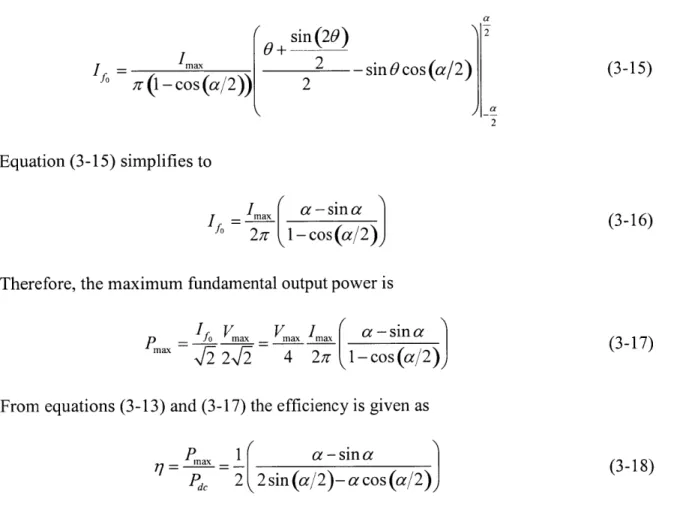
Figure 3-6 plots both the efficiency q and maximum output power versus conduction angle a. This graph was originally reported by Steve Cripps [3]. As expected, class-A mode shows an ideal efficiency of 50%. The efficiency increases as the conduction angle reduced. For a class-B
amplifier, a = ir yields a maximum possible efficiency of 7 = ;T/4 = 78.54%. The efficiency
continues to increase as the conduction angle is reduced further into class-C mode.
This plot shows a very interesting point. Between class-A and class-B modes, the maximum fundamental output power is approximately constant while the efficiency improves from 1/2 to
r/4. When the conducting angle is reduced further into class-C mode, the efficiency increases and approaches a perfect 100% when the conduction angle reaches 0*. However, the efficiency improvement is accompanied by a substantial reduction in the fundamental output power. In modem technologies, especially integrated circuits, power usually comes as a premium.
Therefore, integrated circuit power amplifiers rarely operate in class-C mode because of the low maximum output power.
100
Efficiency 1l (
7: 0---50
0_j Max Output Power
-2e
N
-5
---
4----4---A AB B C Conduction A ng1e
Figure 3-6: Efficiency and Maximum Output Power (Normalized to Class-A) vs. Conduction Angle
By making amplifiers more efficient with reduced conduction angle modes, we not only give up gain but linearity as well. Clipping effects on the output current waveforms introduce
nonlinearities at the output. We can analyze these nonlinearities quantitatively by calculating the high order harmonics components of the output currents. The nth order harmonics can be written as,
-12
1
max(Cos
0 - Cos (a/2))Inf =- I, cos (nO)dO = - cos (n0)dO (3-19)
rc r -a/2 1- cos (a/2)
Using the above expression, we can determine the harmonic components of the output current as functions of the conducting angle. Results of the dc and the first five harmonics components are listed in Table 3-2.
Table 3-2: DC and Harmonics Components of Output Currents in Reduced Conduction Angle Operation Modes Expression Class-A a = 27r Class-AB a = 3;f/2 Class-B a= fT I 2sin(a/2)-acos(a/2) Im I(3r+4) m DC 2ff 1-cos(a/2) 2 2r (2+[) /
Fundamental max a-sina I Ima (3r +2) 'max
27 Il-cos(a/2) 2 2/T(2+V-2) 2
I (1-cosa)sin(a/2) Imax 2Imax
Secod m"x ___'"
3;r (l- cos (a/2)) 3r (l+ -,12 3;r
Tm&X (l-cosa)sina
-max-6fr (l-cos(a/2)) 3f (2+ 2)
Im. (5sin(3a/2)-3sin(5a/2)) 2Imax 21max
ou 60fr (l- cos (a 2)) 15ff (I+ V) 15r
Fifth im (3 sin (2a) - 2sin (3a)) 0 -1f ax
60;T (I -cos (a/2)) 15;T (2+ N2 X a: N C
z3
UiA
0.5
0 --- Fundamental DC 27r r 0 A AB B C Conduction Angleobservation that between class-A and class-B conditions, the fundamental output power is approximately constant. As we reduce the conducting angle, the dc current decreases which explains the efficiency improvement. This is accompanied by the increases in harmonics. The second harmonics dominates throughout the conducting angle range. One interesting
observation is that between class-A and class-B conditions, only the second harmonic is
substantial, all the higher order harmonics are small. Therefore, by biasing the amplifier toward class-B condition in a differential configuration we can significantly improve the efficiency while suffer little setback in linearity.
4 Biasing Techniques
In this chapter, we will study three different fixed biasing topologies: current mirror network, diode-connect, and cascode current mirror. We analyze each topology by addressing the following questions:
Li How does it work? We will discuss the role of each component in the biasing circuit, and ultimately derive the expression to determine the power transistor quiescent current. L What are the effects of the biasing circuit on the gain, linearity, and efficiency of the
amplifier stage and how do we control these effects? By answering this question, we can show the tradeoff in optimizing the circuit for a specific performance requirement.
Finally, we will look at the proposed adaptive biasing topology and study how it improves the efficiency of the overall power amplifier stage.
4.1 Current Mirror Network
VCC
Q
202
U-1X nRj,W Rb RF In IQ0 nX Output Matching R load4.1.1 How does it work?
Luo and Sowlati [5] reported a very popular power amplifier biasing circuitry is shown in Figure 4-1. This conventional biasing technique uses the power transistor
Q
0 as part of a current mirror network. TransistorsQ
andQ,
form a 1: n current mirror network based on their size ratio. TransistorQ
2 provides base current correction for this current mirror network. The baseresistors Rb and nRb provide negative feedback to set
Q
's collector current. To see how this feedback mechanism works, consider the base-emitter loop equation acrossQ
andQ,
as shown in Figure 4-2.bias bias
Figure 4-2: Base-Emitter Voltage Loop
I cI
nc
b b Rb
VbeO± RV +-inRb (4-1)
where
Vbe0 andVF are Qg and Q base-emitter voltage, respectively,
V VI
Ic and
re
beOQ'and Q=
baemtervtgspelyIcO = 1O exp and I= "e) exp bel are
Q0
andQ, collector currents,
VT VT
,8 is the dc current gain of the transistors.
An obvious solution for the above equation is cO = nI,, where VbeO Vbel Consider, however,
the case when V eo drops below V,,. The voltage across resistor Rb will increase which forces more current into transistor
Q
0 's base. This extra base current increasesQ
0 's collector currentby a factor of 6 which, in turn raises VbeO back up.
Similarly, when Vkeo rises above Vbel, the voltage across Rb is smaller. This leads to smaller base and collector currents for Q, which reduces VbeO . Therefore,
Q
collector current IC isQ1,
we can set the quiescent collector current for the power transistorQ
0 while minimizing the current consumption by the biasing network.Resistor Rbias sets the dc collector current for
Q,
. Ignore the base current and the voltage dropsacross the base resistors, we have
(4-2)
I ~I -(VC -2VBE (on)
c1 bias ~R
Ria
Therefore,
Q
0 collector current is determined by(4-3) c=n (Vcc --2VBE(on)
IcO
Rba
The bypass capacitor C, is used to short out any RF signal might present at transistor
Q,
's collector preventing the current bia, from being modulated by the RF signal.4.1.2 Effects on gain, linearity, and efficiency
Vcc Q2 0 , Cl U LL-Qi nRb Output X Rb Matching RF In Zbias Rbacj Z nx - /gM2 Looking into Q2's emitter
nRb
:j77zbiasFigure 4-3: Small Signal Equivalent Circuit for Conventional Biasing
Let Zbi,,, and Z,, be the small signal equivalent resistances of the biasing circuit and the power transistor, respectively, as shown in Figure 4-3. Depending on the resistance ratio Zba
/Z
, a certain portion of the RE signal splits into the biasing circuit, thereby reduces the gain of the amplifier stage. To minimize the biasing circuit's effect on gain and linearity Zbi,,, has to be much larger than Z, .Assuming that the bypass capacitor C, is large enough so that
Q
's collector is at ac ground, from the equivalent small signal circuit for the biasing circuitry in Figure 4-3, we can determineZbias as
Zbias = Rb + (1/gm2
)1
(nRb + r) (4-4)Typically, 1/gm2 is much smaller than nRb+ r, . Therefore, equation (4-4) simplifies to
Zblas = Rb + 1/g. 2 (4-5)
The quiescent collector current of transistor
Q
2 is the sum of the two base currents of transistorsQ0 and Q, .
Ic2 = IbO +Ib] (4-6)
Rewrite in terms of
QO
's collector current and the current ratio n.=c2 2 + Ico (4-7)
Combine equations (4-5) and (4-7)
~RkT n2 kT
Zbis = R +--q = Rb + (4-8)
qIc2 (n+1) qIcO
By selecting the appropriate value for the base resistor Rb and the current ratio n, we can make
sure that Zbia, is much larger than Zn so that the biasing circuit does not affect the RF drive signal feeding to
Q
0 's base. However, there is a limit of how big Rb can be. The base current of a power transistor could be several milliamps. If we make Rb too big, the energy loss due to Rbis significant. In addition, the voltage drop across Rb could reduce the overall voltage headroom and invalidate the initial assumption of negligible base resistance voltage.
With regard to efficiency, the biasing circuit should consume as little energy as possible. By increasing the scaling ratio n of the current mirror, we can reduce the current used in the biasing circuit. However, the dependency of
Q
0 's collector current on process variation in Rbias , Rb andQ, is also scaled by n. Therefore, there is a tradeoff between reducing the current needed for the biasing circuit and keeping the process variation tolerable.
4.2 Diode-Connect
VCC Output Matching di 0 RF InFigure 4-4: Diode-Connect Biasing
4.2.1 How does it work?
Kawamura, et al, [6] proposed diode-connect biasing circuit shown in Figure 4-4. Transistor Q,
is diode-connected with a series base resistor Rb . Ignore Q, 's base current, the current through
Rbias is
'bas = VcC - 2VBE(on) (49)
Rbias
,bias is the base dc current of transistor Q,. Therefore, Q 's collector current is determined by
'cO = cc -2VBE(on) (4-10)
The bypass capacitor C, is used to short out any RF signal at transistor Q 's collector preventing the current 'bias from being modulated by the RF signal.
4.2.2 Effects on gain, linearity, and efficiency
Again, let Z,, and Zbia, be the equivalent input resistances of the biasing circuit and power amplifier, respectively.
VCC R,,OuputD M0chn RFi _C biaU ZL Rb V 711
r
7rgM
1 V 7T it x biasVFigure 4-5: Small Signal Equivalent Circuit for Diode-Connect Biasing
Assuming that the bypass capacitor C, is large enough so that
Q,
's collector is at ac ground, the small signal circuit for the biasing circuitry is shown in Figure 4-5. To find Zbi,,, we apply a test voltage toQ,
's emitter. Kirchoff current law atQ,
's emitter givesr, bV r,,, + Rb
(4-11)
(4-12)
(4-13)
Q,
's collector current is simplyQ
0 's base current. Therefore, equation (4-13) can be rewritten as(4-14)
Zbias - T + Rb
qIco 8
From equation (4-14), we can see that by selecting an appropriate value for Rb we can make
Zbia, sufficiently larger than Z,, to make sure that the biasing circuit does not affect the gain of the amplifying stage.
The biasing circuit does not consume any extra current beside the base current for the power transistor. Therefore, it does not affect the overall efficiency of the amplifying stage.
Or V b IX = - V + r., + Rb Therefore IX(1+p8) V r,, +Rb V rf +Rb 1 Rb b Ias - _g, i___ _ _ 1+ Ix 1+,8 gm, /6