Control and Application of a Pixel-Parallel
Image Processing System
by
Gary Hall
B.S. Electrical Engineering
University of Florida, 1994
Submitted to the Department of Electrical Engineering and Computer Science
in Partial Fulfillment of the Requirements for the Degree of
Master of Science in Electrical Engineering and Computer Science
at the
Massachusetts Institute of Technology
February 1997
© Massachusetts Institute of Technology, 1997 All rights reserved.
Signature of Author
De artment of Electrical Engineering and Computer Science December 4, 1996
Certified by
Accepted by
Prof. Charles G. Sodini Professor of Electrical Engineering and Computer Science Thesis Supervisor
Prof. Arthur C. Smith, Chairman
...
.. ... Department Committee on Graduate Students
Control and Application of a Pixel-Parallel Image Processing System
Control and Application of a Pixel-Parallel
Image Processing System
by
Gary Hall
Submitted to the
Department of Electrical Engineering and Computer Science December 1997
in Partial Fulfillment of the Requirements for the Degree of Master of Science in Electrical Engineering and Computer Science
Abstract
This thesis deals with the design and implementation of a control path for a Pixel-Parallel Image Processing system. This system uses high-density parallel processors (HDPPs) with a processor-per-pixel architecture to perform efficient manipulations of data. To do this, it employs SIMD (single instruction, multiple data) techniques well suited towards many image-processing algo-rithms. This system has been designed with low cost as a primary goal, such that it may be used in a consumer market for which typical parallel-processing systems are prohibitively expensive. The control path must be capable of delivering instructions to the processor array at the highest speed the array is capable of supporting. It must also be able to interface with an inexpensive workstation as the host computer and human interface. These two requirements necessitated some form of instruction expansion from the host-controller interface to the controller-array inter-face, in order to achieve the bandwidth amplification called for.
Previous work has been done on a control path for a similar system, using a content-addressable parallel processor (CAPP) to build the processor array. This controller was designed for 10 MHz operation, which would suffice to support the CAPP array. However, new research has yielded the HDPP array, which uses more dense design and clock rates of up to 20 MHz. A new control path has been constructed to support the increased instruction rate requirements of this processor, as well as address several issues remaining with the previous control path design. In addition, fur-ther work has been done to generate useful image processing primitives, which have been designed for use in more complex image processing applications.
Thesis Supervisor: Charles G. Sodini
Control and Application of a Pixel-Parallel Image Processing System
Acknowledgments
First, I'd like to thank Charlie Sodini, for the opportunity to work with him and his students, and for having good advice about the real world. The time I've been in the group has been a great combination of school and practical work experience, and I'm glad to have been a part of it. I also owe a large debt to Jeff Gealow, who I worked closely with during the course of this research. While it's true that, on occasion, I did him some favors and answered a few questions, I'm quite sure I'm very far from catching up to the number of times he's helped me. I appreciate his patience in dealing both with tricky hardware questions and stupid UNIX questions, which occurred with roughly equal frequency.
Then there's the tons of fellow researchers who I have enjoyed spending time with over the last year or so. Joe Lutsky, Jen Lloyd, Steve Decker, and Jeff have provided endless hours of amusing conversation over WhoppersTM and fries. There have also been many evening dinners with them, Andy Karanicolas, and Dan Sobek, where I learned lots of interesting tidbits about industry, and discovered the joy of pan-fried rays. To Mike Perrott, I owe debt for most of the exercise I man-aged to get at MIT, and earned a healthy respect for road bikes in a head wind. And to bring back a blast from the past, thanks to Daphne Shih, for showing me the ropes at MIT, and being the first good friend I had here.
Thanks to Iliana Fujimori, her brother Marco, MeeLan Lee, Howard Davis, and Tony Cate for getting me out of my dorm room every once in a while, and showing me most of what I saw of the social scene in Boston. I had fun every time we went out, and I'll miss that part of Boston a lot. I'd also like to thank some friends at Ashdown, for going hiking, eating dinner, wasting time watching TV, and even studying once in a while. I can't list them all here, but thanks to Laura Johnson, Tom Lee, Pat Walton, Rebecca Xiong, Kathy Liu, and John Matz, who were the main culprits in forcing me out of my room to have a life.
I'd like to thank my bosses, mentors, and friends at Motorola for making this return to grad school possible. To Neil Eastman and Jerry Johnson I owe special thanks. I'll always appreciate their hard work and special attention that got me here, and I hope that in the future I can repay both of them in some way. I also thank Rae Zhang, Phil Teeling, Dave Melson, Hsi-Jen Chao, and Sandhya Chandarlapaty for guidance and advice when I worked with them. I also want to include Jason Robertson, Jerry Hsiao, Harry Chow, Tod Hufferd, Greg Coonley, and Mike Weatherwax, for being about the coolest group of people to hang out with after work that ever was, and keeping me going through grad school even though they knew they were having more fun.
Control and Application of a Pixel-Parallel Image Processing System
had the epiphany that happens to everyone at some point, when I realized how smart they were, and how ignorant I was, in many facets of life. They got me started along the right path, helped me keep going when I was ready to quit, and gave me just the right amount of support along the way. If I can remember half of what they taught me, and apply that half as well as they did, I'll consider myself a success in all ways that matter.
Control and Application of a Pixel-Parallel Image Processing System
Table of Contents
Chapter 1
Introduction
1.1 1.2 1.3 Background ... 15Controlling a Real-Time Image Processing System ... 15
Organization of Thesis ... 17
Chapter 2
Controller Architecture
2.1 Previous Work ... 2.1.1 Controller Strategies ... 2.1.2 Controller Model ... 2.2 Hardware Implementation ... 2.2.1 VMEBus Interface ... 2.2.2 ControlPath ... 2.2.3 Data Registers ... 2.2.4 Microprogram Unit ... 2.2.5 Host-Controller Interface .. 2.2.6 Control Store... 2.2.7 Memory Refresh Interrupt ....
19
...
19
... 23 ... 24 ... 24 ... 26 ... 27 ... 29 ... 31 ... 33 ... 35Chapter 3
New Controller Requirements
39
3.1 Decreasing Board Size... 3.1.1 PCB Technology ... 3.1.2 Logic Integration... 3.1.3 Logic Modification ... 3.1.4 Results of Integration/Modification ... 3.2 Increase System Speed... 3.2.1 10 MHz Controller Critical Path ... 3.2.2 Sequencer I-Y Correction ... 3.2.3 Sequencer CCMUX Correction ... 3.2.4 Opcode Register Output Enable Correction .. 3.2.5 Controller Idle Loop ... 3.3 Increasing Controller Robustness ......
39
...
39
... 40 ... 40 ... 42 ... 44 ... 44 ... 45 ... 47 ... 49 ... 50 ... 5119
Control and Application of a Pixel-Parallel Image Processing System
Chapter 4
Software Application Framework
4.1 Framework Abstraction Levels ...
4.1.1 Application Programmer's Interface ... 4.1.2 Hardware Abstraction Level ... 4.1.3 Hardware Interface Level ...
4.2 Software Simulators... 4.3 Application Writing ...
4.3.1 Initialization Overhead ...
4.3.2 Sequences and Code Generators ... 4.3.3 Presequences and Control Instructions ... 4.4 New Applications... 4.4.1 Edge Detection ... 4.4.2 Template Matching ... ... 55 ... 55 ... 56 ... 58 ... 58 ... 59 ... 59 ... 59 ... 61 ... 62 ... 62 ... 64
Testing and Results
5.1 5.2 5.3 5.4 Board Production Problems ... Clocked Testing ... ... Interrupt / Memory Write Conflict ... Perform ance Analysis ...69
. 69
.70 .72 .7377
6.1 Accomplishments ... 77 6.2 Future Work ... 78 Appendix A Test Points / Jumper Positions 81Appendix B
Board Documentation
B.1 Controller Board Schematics ... 8383
55
Chapter 5
Chapter 6
Conclusions
Control and Application of a Pixel-Parallel Image Processing System
B.2 EPLD Internal Schematics ...
83
B.3 Pertinent File Information ...
83
B.3.1 ABEL Files ... ... 83
B.3.2 Conversion of ABEL to PDS ... 83
B.3.3 EPLD Simulation Files ... 84
B.3.4 Other Important Files ... 84
Appendix C
Software Maintenance
85
C.1 Com pilation ... ...
85
C.2 XAPP Structure ...
85
Appendix D
Template Matching Application Code
89
D.1 Method 1 - Maximum Speed ...
89
D.2 Matching 2
-
Maximum Template Size ...
92
Control and Application of a Pixel-Parallel Image Processing System
List of Figures
1-1: Block Diagram of Image Processing System ... 16
2-1: Direct Control From Host (System I DBA) ... 20
2-2: Complex Microcontroller (System II DBA) ... 20
2-3: Current Controller Strategy ... 22
2-4: Instruction Selection ... 23
2-5: Controller Implementation Model...24
2-6: VM Ebus Interface ... 25
2-7: Control Path ... ... 26
2-8: Microprogram Unit Architecture...29
2-9: 10 MHz Controller Control Store ... 34
2-10: Old AIM, CIM Instruction Formats ... 35
2-11: New AIM, CIM Instruction Formats...36
3-1: FPGA CLB Architecture ... 41
3-2: EPLD (XC7300) Device Block Diagram ... 42
3-3: Critical Paths of 10 MHz Controller ... 45
3-4: Critical Path Fix ... 46
3-5: VM E W rite Cycle ... 52
4-1: Programming Framework Overview ... 56
4-2: Programming Framework Abstraction Levels ... 57
4-3: Edge Detection...63
4-4: Template Matching Algorithm ... 64
4-5: Parallelizing Template Matching ... 65
4-6: Template M atching...67
5-1: VME MODSEL Timing Problem ... 71
5-2: Controller Performance Comparison...74
A-1: Test Point Location ... 81
Control and Application of a Pixel-Parallel Image Processing System
List of Tables
2-1: Controller Status Register Bits ... 27
2-2: Low-Level Host-Controller Interface Operations ... 31
3-1: Part Count Comparison ... 42
3-2: PLD Integration Results ... 43
3-3: Expansion of a Conditional Branch...49
3-4: Idle Loop Code Expansion ... 51
4-1: Controller Instruction Interface Functions ... 61
5-1: End-to-End Bus Transaction Delays ... 70
5-2: Application Performance with HDPP Array ... 75
Control and Application of a Pixel-Parallel Image Processing System
Chapter 1
Introduction
1.1 Background
Image processing in real time presents many difficulties for most general-purpose computers. The most serious of these is the well-known von Neumann bottleneck, which requires the proces-sor to individually access each data element (usually a pixel in this context). Doing image pro-cessing with this type of machine would require an exceptionally fast general-purpose computer, as even a modest-sized image of 256 x 256 has 65,536 pixels which would all be processed sepa-rately.
Many image processing tasks today can be implemented to take advantage of data parallelism, which is a method of assigning one processor to each data element and performing all operations on the data in parallel [1]. This is known as single-instruction-multiple-data (SIMD) processing. This method has given rise to several forms of parallel processors, which have a much higher pro-cessor-to-memory ratio than general-purpose computers. The Connection Machine [1] is an example, with up to 64K processing elements (PEs), with each PE having up to 64K bits of mem-ory (in the CM2). The fully configured CM2 requires four front-end host machines, as well as a
data vault, to house the processor memory and provide data I/O.
However, this type of machine is too expensive for many common applications in industry. The expense of the processor itself is significant, and the overall system expense is such that it would be impossible to produce a reasonable consumer application containing this technology. This has given rise to new research on inexpensive systems that still take advantage of data parallelism, while having a simpler interface, more integration, and maintaining real-time performance.
Researchers at MIT have developed a system to meet this goal, using processors with a 16 x 16 internal PE array and content-addressable memory [2]. This system demonstrated efficient image processing with parallel-oriented tasks, but did not include a complete real-time image I/O mech-anism. Further research is currently being conducted on a high-density parallel processor (HDPP) which contains 64 x 64 PEs on chip [2]. There is also a corresponding system design to allow image I/O at frame rate (30 frames/sec), as well as a simple programming interface. Figure 1-1 shows a block diagram of the system. A new architecture for the Control Path in this system is the subject of this thesis. Software applications demonstrating some capabilities of the system to per-form useful image processing in real time are also shown.
1.2 Controlling a Real-Time Image Processing System
Control and Application of a Pixel-Parallel Image Processing System
)ntrol
)ntrolath
_F
\ II C MImagerADC
0 0 4-6CV
o8
Processed
Images
o Ll. o I.J..Image
Data Path
Figure 1-1: Block Diagram of Image Processing System
fast enough to place the bottleneck on the processors themselves, not on the control path. As most of the design time and expense on this type of project was devoted to these processors, one would prefer to get the most out of the processing power they present. Second, for a project of this scope, the controller had to be kept to a low expense. For a system to be commercially viable, it cannot be in the high price range of typical research systems for image processing in real time. Finally, it had to be small enough to be practical in the real world. A typically successful recipe in going from research to practice is smaller, faster, cheaper; though for this application, machines such as the CM2 and successors are so fast that a practical system can be much slower.
The primary function of this controller was to deliver sequences of array instructions to the pro-cessors fast enough to keep them busy as much as possible. In addition, certain other functions of the system fell under the controller's responsibility, such as any memory refreshes of the proces-sors' internal DRAM, supervising and synchronizing image I/O between the array and the datap-ath hardware, and providing an interface between the system itself and the top-level application programmer.
One part of this research was to complete the next evolution of a controller for use in a pixel-par-allel image processing system. The previous controller, designed by Hsu [3], was used in an image processing system employing the aforementioned CAPP array. The controller resides in the system built by Hermann and Gealow [2] around their image processing arrays. This system
Control and Application of a Pixel-Parallel Image Processing System
includes both the hardware shown in Figure 1-1, as well as an extensive amount of software sup-port. This software consists of simulators, to build and test application code on the system, and hardware interface code, to allow programmers to run image processing tasks on the system with-out a detailed knowledge of it's internal architecture.
There were three primary requirements to be met by this new controller, to be discussed in more detail in later sectionsý
* Decrease board size -the controller must fit completely inside a standard double-height VME chassis
* Increase system speed from 10 MHz to a target of 20 MHz -the new array processors will have a higher clock rate than their content-addressable counterparts
* Increase controller robustness -the previous controller exhibited intermittent problems at var-ious clock frequencies, including the target of 10 MHz
Due to the large amount of software support for the previous controller's architectural model, it was advantageous to remain as similar as possible to that model, while still meeting the new requirements. This thesis documents the similarities and the differences between the two control-ler implementations.
In addition, a part of this research demonstrates the viability of this system, with some basic image-processing tasks. Several of these programs have already been written, to do tasks such as smoothing and segmentation, median filtering, and optical flow, on static images. This research extended these operations to real-time images, and produced new operations such as edge detec-tion and primitive template matching.
1.3 Organization of Thesis
This chapter outlined the primary goals of this research, with some background on parallel pro-cessing methodologies. It introduced the concepts of SIMD propro-cessing and parallelism, and
pre-sented an overall system for parallel image processing.
Chapter 2 discusses the architectural model of the new controller design. It shows the evolution in controller design for this type of project, and discusses the similarities and differences in hard-ware implementation between this and the previous controller.
The decisions made in meeting the new requirements are discussed in Chapter 3. It includes an in-depth analysis of the critical paths of both the old and the new controller, outlining problems that were fixed with this design. It also presents some of the logic that went into the decision of what strategy to use for new logic integration.
Chapter 4 deals with the software application framework. It describes the interface provided to programmers creating applications on this system. It includes some tips on efficient use of resources in applications, and details some new applications written as part of this thesis.
Control and Application of a Pixel-Parallel Image Processing System
The testing of the controller and results are described in Chapter 5. This chapter shows some of the pitfalls encountered with this design, some problems in board fabrication, and workarounds. It also includes the quantitative results in execution speed and a comparison to the previous con-troller.
The final chapter of this thesis is the conclusions from the work done, and a short description of where future work might lead. Following that are several appendices provided for reference on details such as board test points and organization of files used in this thesis (source code, board schematics, etc.). This includes pointers to documentation on that source code and details of the controller hardware.
Control and Application of a Pixel-Parallel Image Processing System
Chapter 2
Controller Architecture
As mentioned in the introduction, one of the attributes of this controller is a design that is much simpler, and whose cost is much lower, than the sophisticated controllers used in expensive mod-em parallel-processing machines. This goal was accomplished by Hsu [3] in a previous thesis. This new design has other goals to be discussed later, but also sought to take advantage of earlier work done in this area.
To this end, the controller built for this system was designed to be software compatible with the previous design done by Hsu. The programming framework that supports this controller, and the system in general, simulates both bodies in software, and provides a layer of abstraction to the hardware. There is an obvious advantage to staying software compatible at the top-level control-ler model, so that application and high-level interface code may remain unchanged. Along these same lines, the closer the hardware implementation remained to the original, the less modification was needed to the low-level interface code in the framework. However, some changes were required to meet the new goals of the controller design. Therefore, there were some decisions to be made between this hardware/software trade-off. Some of these decisions will be discussed here, and some in the next chapter.
This chapter outlines the main architectural details put forth by Hsu in a previous image process-ing system, which are in common with the new controller. It also discusses changes made in this architecture, for the new controller design.
2.1 Previous Work
2.1.1
Controller Strategies
The controller model used in this design has evolved from work done on previous iterations of this research. A discussion of these previous implementations will help clarify the choices made behind the new controller model. This section summarizes a discussion by Hsu [3] on several controller strategies investigated before choosing a new model.
Figure 2-1 shows a simple control strategy used in the first system constructed by the Associative Processing Project (APP) (predecessor to this research). This system was constructed around a Database Accelerator chip (DBA), and the system was termed System I [4]. The control model used in this system was to have the host computer act as the controller as well, generating low-level instructions to be sent directly to the PE array. This model offers one obvious benefit, in that the "controller" is built almost entirely in software, with the only exception being the interface between the host's bus and the array. There were, however, two key limitations of this approach.
Control and Application of a Pixel-Parallel Image Processing System
Figure 2-1: Direct Control From Host (System I DBA)
The first was that the instructions were generated at run time, which required the host computer to generate instructions as fast as the array could process them. The second limitation was that the system was slowed by the rate at which the instructions could be delivered to the array, through the bus interface. These problems combined to cause the system's performance to be degraded by two orders of magnitude below its potential [5].
The second approach was to use a more complex controller. This model, shown in Figure 2-2, has the host issuing macroinstructions to the controller. The controller then decodes these
Control and Application of a Pixel-Parallel Image Processing System
tions and expands them into nanoinstructions which are sent to the PE array. In interpreting the microinstructions to produce the correct instructions for the PE array, the controller itself locally executes microinstructions. This approach eliminates both of the previous drawbacks, in that the host computer doesn't need to generate many instructions at run time, and the required bus band-width is reduced. This was the method used to build a controller for the second DBA system, System II [5]. System H's controller consisted of a microprogram control store and sequencer, and it's datapath for delivering instructions contained register files, a 32-bit arithmetic logic unit (ALU), a 32-trit1 ternary logic unit (TLU), and control and interface logic. This type of
architec-ture was also used in the Connection Machine [1].
However, this approach was not without its own shortcomings. In this model, the controller is a microprogrammed machine. It stores array instructions in a writable control store, allowing dif-ferent array architectures to be used, with arbitrary instruction widths and formats. However, to be able to generate these instructions at a sufficient rate, the controller must be very fast and com-plex. System II's data path needed expensive and sophisticated components, the 32-bit ALU and 32-trit TLU, in order to generate the instructions fast enough to avoid the DBA chips becoming idle. This approach also greatly complicates application development for the system. In addition to writing code for the application itself, the microprograms on the controller must also be devel-oped.
A new, simpler controller model was set forth by Gealow et. al. [2], which still draws upon the idea of amplifying the bus bandwidth using a form of instruction expansion. However, this new model focuses more on a simple, inexpensive implementation that can still meet the speed requirements of the processors being used in this research. One of the new ideas for this model was generating the sequences of array instructions at compile time, instead of run time. This reduces the need for a datapath in the controller, since the instructions are not generated on the fly. This new system architecture is shown in Figure 2-3. In this new architecture, the sequences of instructions (similar to procedure definitions) are stored in the controller. The host computer then simply calls these sequences at run-time, much like calling procedures. As noted by Gealow et. al., this type of system poses two problems for this system's designer:
* Run-time scalar data. Any sequences that depend on the use of data generated at run
time (such as variables) would, in the simplest implementation, require the data to be compiled into the instruction stream. This would necessitate instruction generation on-the-fly.
* Run-time flow control. If the flow of program execution depends on results generated
at run time, the instructions cannot be generated at compile time.
In a general sense, these problems would be very difficult to overcome. However, the fact that these processors are implemented in a bit-serial fashion gives some unique possibilities to circum-vent the problem.
Control and Application of a Pixel-Parallel Image Processing System
Figure 2-3: Current Controller Strategy
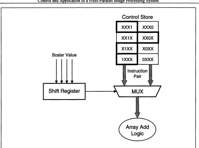
In the important case of bit-serial arithmetic, a solution to the first issue is instruction selection. Consider the case of adding a run-time scalar to an n-bit value stored in the array. One simple solution would be to generate a sequence of instructions for all 2n possible scalar values, but clearly this is not acceptable for any significant value of n. However, most bit-serial algorithms can be broken down into pairs of instructions, one pair per bit. A simple case of this is shown in Figure 2-4, for a four-bit addition. The example shown is adding the binary value 1101. The sequence for adding 1 is stored in one portion of the control store, and another sequence for add-ing 0 is stored in another portion. At run-time, the scalar value is loaded into a shift register on the controller. This register then controls which instruction is sent to the array. The value is loaded in the shift register, and appropriate instructions are sent to the array. Practically speaking, the hardware can be further optimized, since a MUX of the width of the control store (32 bits for this controller) is impractical, but this diagram shows the model used.
The problem of run-time flow control is more complicated. In previous processors, which were associative, a mechanism called responder feedback was used to solve this problem [2]. Each processing element would provide a one-bit input to a response resolver. This resolver would per-form a logical OR operation on its inputs, allowing Some/None operations to be done, which is a common feature of associative processors. One example of the usefulness of this mechanism to remove the need for run-time flow control is a maximum value computation. Without the response resolver, a program would have to traverse a binary tree of maximum values. For instance, it would first check for PEs with 1XXX. If none were found, it would check for 01XX; otherwise, it would check for 11XX. This would continue, and this program's flow is clearly dependent on the results of run-time generated data.
With the response resolver, this dependent flow is not necessary. First, all processing elements are active. A match is performed on 1XXX. Processing elements that match this value are left acti-vated, while the rest are turned off. The response resolver is used to determine if any PEs
array instructions sequence calls
Control and Application of a Pixel-Parallel Image Processing System
Figure 2-4: Instruction Selection
matched -- if not, then the previously active PEs remain active. The output of the response resolver is then shifted into a serial output register that will contain the maximum value. Succes-sive matches are then performed on X1XX, XX1X, and XXX1. The PEs still active contain the maximum value, and the output register contains this value.
However, in the most recent version of the parallel processor being used with this controller, the response resolver is not present. Hardware exists to activate certain PEs based on various criteria, but there is no Some/None feature present to determine if any PEs are currently active. This means that run-time flow control for some algorithms is not possible, or not as efficient, as with architectures supporting the response resolver. However, as we will see in Section 4.4.2, for some important algorithms, efficient software solutions can be created to get around this problem.
2.1.2
Controller Model
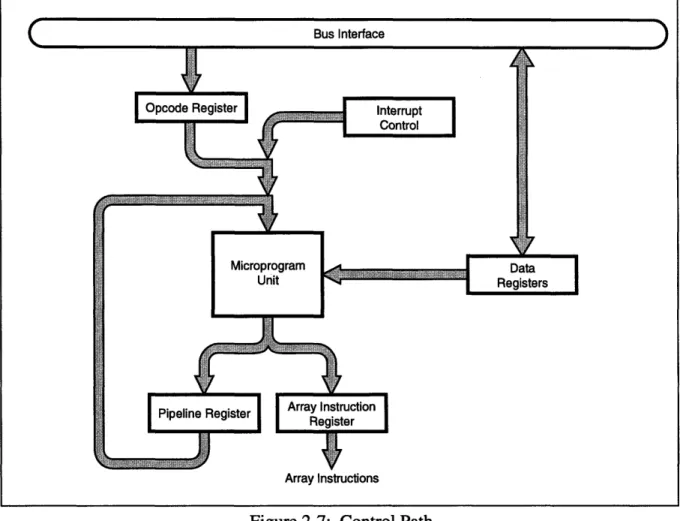
The final model for the controller implementation is shown in Figure 2-5 [2]. This figure shows the various components that were part of the previous controller, and kept in this implementation for software compatibility. This model is that seen by the software framework, but in this control-ler, certain parts of the model are merely a layer of abstraction.
Control Store
Control and Application of a Pixel-Parallel Image Processing System
Array Status Values Array Instructions
Figure 2-5: Controller Implementation Model
2.2
Hardware Implementation
2.2.1
VME Bus Interface
The details of the bus interface are largely unchanged from the previous implementation of this controller. Due to this fact, and the fact that bus interface is a fairly common and simple part of any system connected to a proprietary bus, the reader is referred to previous work for many of the details of this portion of the design [6], [3].
In this system, the host SPARCstation, along with the PT-SBS915 (the VME chassis used in this system) act as the VMEbus master The controller board is the VMEbus slave. Because the con-troller has no need of external interrupts or block data transactions, the only transfers supported is read and write. Specifically, the bus interface is designed to support only 32-bit transfers, in
Control and Application of a Pixel-Parallel Image Processing System either user or supervisor mode.
For choice of address space, attention was paid to the other two VMEbus slaves designed as part of this research: the previous controller board, and the data path board [7] shown in Figure 1-1. Each of these boards occupy some of the available 32 bits of address space, ideally a few addresses each. The previous controller decoded eight bits of the VME address for comparison to a base address, occupying the addresses of FXXXFX00-FXXXFXIF. This design uses the same base address, to reduce the software changes to the VMEbus driver for the controller. The datap-ath board occupies address space XXXXAX00-XXXXAX1F (decoding only four bits for the base address).
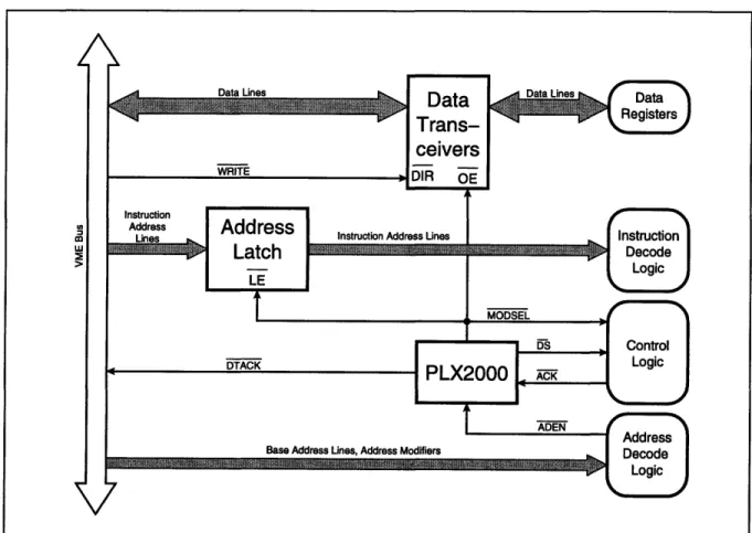
Figure 2-6 shows the VMEbus interface implemented in all of the slave modules used in this research project to date. The PLX2000 chip interfaces directly with the VMEbus, signalling the
Figure 2-6: VMEbus Interface
start of a data transfer with MODSEL (module select) and its completion with DTACK (data transfer acknowledge). DS (data strobe) indicates valid data is present on the bus data lines. It uses ADEN (address enable), a signal asserted by the slave module when the address lines and address modifiers indicate a bus transfer for this module.
Control and Application of a Pixel-Parallel Image Processing System
EPLDs (erasable programmable logic devices). The reasoning behind this is discussed in depth in Section 3.1.2. Address decoding and the other interface signals to the PLX2000 were also done in these EPLDs.
2.2.2
Control Path
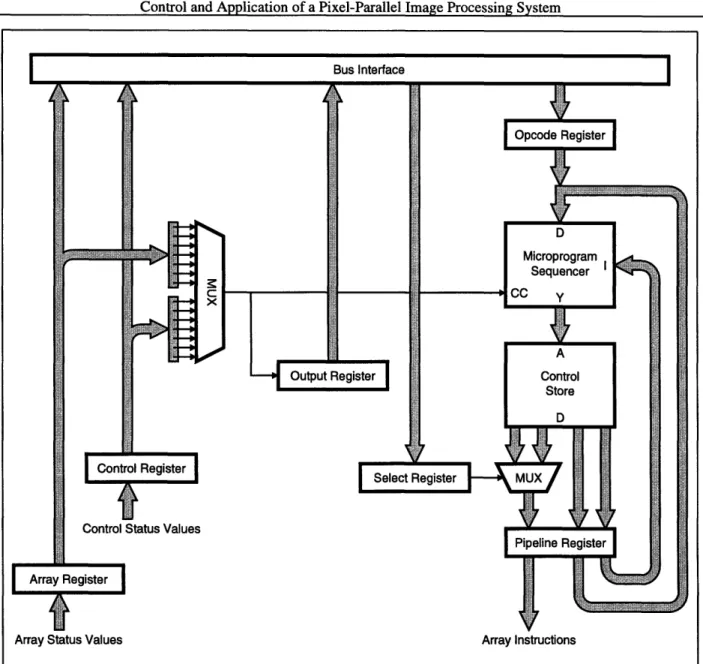
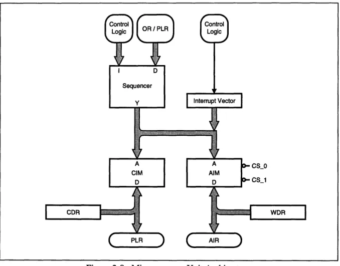
The control path is responsible for accepting control instructions from the host, and delivering array instructions to the array. Figure 2-7 shows the components of this path. The host computer
Figure 2-7: Control Path
writes the address of a sequence to be launched into the Opcode Register (OR). The Micropro-gram Unit is the most important part of this path, containing the Control Store (holding the instructions for the array and the controller), and the Microprogram Sequencer, which controls program flow on the controller. The data registers allow programming of the microprogram unit and interrupt control, and also serve as a method of returning controller status, array status, and other array output to the host computer.
The Interrupt Control mechanism here differs significantly from that of the previous controller. In that controller, interrupt control was a very complicated part of the architecture, supporting multi-ple priority interrupts, nested interrupts, and masked interrupts. In this immulti-plementation, it was decided to use the interrupts explicitly for refreshing the DRAM in the array processors. This was
Control and Application of a Pixel-Parallel Image Processing System
due to the fact that the interrupt control was not used in the previous controller, never having been tested, and therefore memory refresh was the job of the programmer, who had to explicitly place a memory refresh sequence as part of the application.
2.2.3
Data Registers
As mentioned, one of the goals in implementing this controller was to stay software-compatible with the previous controller to as large an extent as possible. One way of achieving this goal was to make the data registers the same in both controllers, which makes the input/output interface of both controllers the same. For the sake of completeness, the description of the data registers is included as part of this thesis.
The Controller Status Register (CSR) is a read-only register containing various status bits from the controller. The host computer reads this register to determine what state the controller is in, and determine what operations it is ready to handle. Table 2-1 shows the make-up of the CSR.
bit 7 6 5 4 3 2 1 0
Table 2-1: Controller Status Register Bits
The reserved bits are currently tied to ground. The meaning of the bits are as follows:
REFRESH signifies that the controller is currently performing a memory refresh operation. For the most part, this bit is used by the controller itself, to control the interrupt logic and the memory programming logic. However, this bit is available for the host to read. This is the only bit in the CSR that is active low (that is, this bit is 0 if a refresh is currently being performed). Note that, due to the method for programming the control store (explained later), it is unsafe to attempt a memory write while a refresh is occurring. But in order to stay software compatible with the pre-vious controller (which did not have this status bit), and to avoid race conditions where a refresh occurs between a CSR read and a memory write, this problem is resolved in hardware.
WMEMBUSY (write memory busy) shows the status of memory writes in the controller's Con-trol Store. This bit is 1 if a memory write to the ConCon-troller Instruction Memory (CIM) or Array Instruction Memory (AIM) is currently pending or active. The host should read this bit before attempting another memory write -- this checking is done in the software framework, transparent to the application programmer.
DIBUSY (direct instruction busy) contains status pertaining to Direct Instruction operations on the controller. If the host has sent an array instruction directly to the array, bypassing the Control Store, this bit stays active until the instruction has been successfully delivered. The framework reads this bit before attempting another direct instruction, or a memory write.
Control and Application of a Pixel-Parallel Image Processing System
automatically upon the launch of a sequence, and cleared by the software framework at the com-pletion of each sequence. This bit is read before attempting a memory write.
APBUSY (associative processor busy) is used when, during a sequence, the array is placing a
value in the Output Shift Register (OSR). This bit is high until the value is valid to be read by the controller. The name is an artifact of the previous system, which used associative processors. This bit is set at the start of each sequence, and cleared by the software framework when the out-put is valid. It is also checked before attempting a memory write.
GO signals the host that a sequence is currently pending. This will occur if one sequence is
run-ning, and the host launches another sequence. This sequence will be saved in the Opcode Regis-ter until the previous sequence completes. The framework checks this bit before launching a
sequence.
The Array Status Register (ASR), a read-only 8-bit register, contains status bits from the array, used by the controller in special situations. This mechanism provides for some limited run-time flow control with sequences created at compile time, limited in that the array can only provide certain status bits in the ASR. One use of this register is to forward status signals from the data path board to the controller, which controls the handshaking during image I/O.
The Select Shift Register (SSR) is the write-only 32-bit register used to perform the instruction selection mechanism shown in Figure 2-4 on page 23. The input operand is loaded in parallel into the register, and the LSB of this register is used to select an instruction from part of the AIM (either AIMO or AIM1, depending on the bit value).
The Output Shift Register (OSR) is the read-only 32-bit register that allows the host to read vari-ous data outputs from the array. This shift register's input is tied to a 16:1 multiplexer, which also serves as the input to the sequencer's Condition Code (CC) bit (to control conditional branches). This register is generally written by array assembly code, transparent to the application program-mer. The programmer would simply issue the sequence, and then read the OSR, and the frame-work would monitor the status and pend the read until the data is valid.
The Controller Control Register (CCR) functionality has changed slightly since the previous con-troller. Previously, it was a 24-bit register, 16 bits of which were used to load a refresh counter (this mechanism was never used on that controller). Six of the remaining bits were unused, and the last two bits were used to clear the Pipeline Register (PLR) and the Array Instruction Register (AIR), respectively. In this design, the clearing of both of these registers is completely controlled in hardware -they are cleared upon a Reset, and at appropriate times during programming of the controller. The CCR is now a 16-bit write-only register, whose contents are used to load a refresh counter. However, as will be discussed in Section 2.2.7, the behavior of this register and the counter have changed.
The Write Data Register (WDR) is a write-only 32-bit register, used to program the Array Instruc-tion Memory (AIM) porInstruc-tion of the control store. The data to be written to memory is loaded into this register, and another operation provides the address, and does the memory write. This
func-Control and Application of a Pixel-Parallel Image Processing System tion is hidden from the application programmer, in the software framework.
The Control Data Register (CDR) performs the same function as the WDR, providing data to the Controller Instruction Memory (CIM), rather than the AIM. It is written simultaneously with the WDR, and is present only to avoid connecting the data outputs of the CIM and AIM.
The Opcode Register (OR) is an additional data register on the controller. To launch a sequence, the host sends the address in the CIM of the sequence, and signals the controller to branch to this
address. The OR holds this destination address until the sequence has been successfully begun.
2.2.4
Microprogram Unit
The Microprogram Unit consists of the Microprogram sequencer [8], the CIM and AIM, and var-ious control logic. Figure 2-8 shows the architecture of this system component. The Interrupt
Figure 2-8: Microprogram Unit Architecture Vector is a part of the refresh interrupt circuitry, and will be discussed later.
The Sequencer has a four-bit instruction input (I), a 16-bit branch address input (D), and a 16-bit address output (Y). In deciding which address to finally output to memory, the sequencer can choose from several sources. If there is no branching involved, there is an internal program
Control and Application of a Pixel-Parallel Image Processing System
counter that is incremented and sent to the Y outputs. If the instruction is a Return of some sort, the sequencer uses the value on the top of its internal stack (presumably placed there by a gosub or loop instruction). If it is a branch instruction, the sequencer examines the Condition Code (CC) input, as well as the Condition Code Enable (CCEN) input. If these evaluate to a condition allow-ing the conditional branch (either both are TRUE or CCEN is FALSE), the sequencer uses the D inputs as the branch destination, and passes them through to the Y outputs. In this case, the branch destination is part of the PLR, which is enabled by the control logic. Finally, the sequencer can take an address from an external source (here, the OR), enables this source with a MAP output on the sequencer, and passes this value through from the D inputs to the Y outputs. With these resources, there are sixteen control instructions provided by the sequencer. However, only eleven of these were useful in the construction of this system, and were provided interface functions in the software framework (Section 4.3.3). In the following descriptions, any "condi-tional" instruction means that the action is only taken if the CC and CCEN inputs dictate action:
Jump zero (JZ) -It resets the sequencer's stack pointer and causes the sequencer to jump to the very first location in microprogram memory. This is the location of the "idle loop," which then launches the next sequence. This instruction is added by the framework to the end of every sequence.
Jump map (JMAP) -Used to jump to an external "map" register. This gives the application designer added flexibility in branching, where the destination doesn't have to be in the pipeline path. In this system, the OR is used as the map register, and this instruction is used to launch new sequences.
Conditional branch to subroutine (CJS) - This instruction allows the controller to gosub to a subroutine, placing the return address on the stack. This is the instruction used when an interrupt is generated. The destination address is sup-plied from the Interrupt Vector register to the D inputs.
Conditional return (CRTN) -Used to return from a subroutine call.
Conditional jump to pipeline (CJP) - Same as CJS, except that there is no method of returning to the present address. This is the basic jump instruction. Load counter and continue (LDCT) -Part of the Loop...endloop instruction set. This instruction loads the lone loop counter, and continues.
Repeat pipeline, counter != 0 (RPCT) -Used to continue looping N times, this instruction jumps back to the start of the loop until the counter is 0.
Push/load counter (PUSH) - Part of the Repeat...until instruction set. This instruction loads the lone loop counter, and pushes the address of the start of the loop onto the stack.
Control and Application of a Pixel-Parallel Image Processing System
Test end of loop (LOOP) - Tests the condition input, and either jumps to the address on the top of the stack (continue looping), or pops the stack and continues. Used to terminate the repeat...until sequence.
Conditional jump to pipeline and pop (CJPP) - Used as a conditional break from the repeat...until sequence. If the condition is passed, pops the start of the loop from the stack (discarding it), and jumps to the address in the pipeline.
Continue (CONT) - Program flow continues to the next instruction.
2.2.5
Host-Controller Interface
There are several low-level interface functions between the host computer and the controller. All of these functions have higher-level wrappers provided by the software framework, but any com-munication between the host and the controller must go through the register reads/writes shown in Table 2-2. Note that in this controller, 12 functions are used, which is a reduction from 17 in the previous controller [3]. This reduction is due to the fact that the HDPP's instruction word is 27 bits wide, vs. 88 bits for the CAPP, and the reorganization of the Control Store that this fact allowed. To the system software, each of these operations appears as register read or write. The offsets shown are the memory-mapped offsets of the "registers" in the VMEbus interface.
Offset from
Read /
Operand
se fr
Operation
e
Output Size
CSR bits to be checked
Base Addressa Write (bits)b
(bits)b
0
WRTORG
W
16
GO
1
WRTCIM
W
16
GO, ALLBUSY,
DIBUSY, WMEMBUSY
2
WRTAIMO
W
16
GO, ALLBUSY,
DIBUSY, WMEMBUSY
3
WRTAIM1
W
16
GO, ALLBUSY,
DIBUSY, WMEMBUSY
4
GODI
W
32
GO, ALLBUSY,
DIBUSY, WMEMBUSY
5
WRTSSR
W
32
GO, ALLBUSY
6
WRTWDR
W
32
7
WRTCCR
W
16
8
RDCSR
R
8
Control and Application of a Pixel-Parallel Image Processing System
Operand/
Offset from
Read /
Operand
ase
from
Operation
e
Output Size
CSR bits to be checked
Base Addressa Write (bits)b
(bits)b
9
RDASR
R
8
GO, APBUSY, DIBUSY
10
RDOSR
R
32
GO, APBUSY, DIBUSY
11
RESET
W
n/a
Table 2-2: Low-Level Host-Controller Interface Operations
a. Because these transactions are 32-bit operations, where the minimum width possible on the VMEbus is 16 bits, address bits A5 - A2 are used to determine offset. A1 is ignored.
b. All bus transactions are 32 bits; this value signifies the amount of this 32 bits that is used.
WRTORG -Write Origin. This operation takes the operand, which is the address in the Control Store of a sequence, and places it in the OR. It also sets the GO bit of the CSR, signalling the controller to launch this sequence.
WRTCIM -Write Controller Instruction Memory. The operand for this operation is the address of the memory location to be written. The data to be written is taken from the CDR, which should be placed there by a previous use of WRTWDR. WRTAIMO - Write Array Instruction Memory 0. Serves the same function as WRTCIM, but the data is taken from the WDR, and written into AIM0.
WRTAIM1 -Write Array Instruction Memory 1. Same as above, but writes to AIM1.
GODI -Go Direct Instruction. This operation takes the input and sends it directly to the array, without accessing the control store, for a single cycle. In the current implementation, the actual register used is the WDR, as the array instruction width was reduced to 27 bits. Assumes the WRTWDR has occurred previously.
WRTSSR - Write SSR. Writes the input data into the SSR, to be used to select instructions from the AIM.
WRTWDR - Write WDR. Writes a value into the WDR (and the CDR), to be used in a WRT(CIM/AIMO/AIM1) or GODI instruction.
WRTCCR -Write CCR. Uses the 16-bit input to load the top 16 bits of a 24-bit counter, used for the refresh interrupt.
Control and Application of a Pixel-Parallel Image Processing System
RDASR -Read ASR. Reads the 8-bit ASR from the controller.
RDOSR - Read OSR. Returns the 32-bit OSR, whose values are the 32-bits shifted in from the CCMUX.
RESET - Resets the controller. Clears the PLR and AIR until a WRTORG or GODI are executed. Stops refresh interrupts from being generated until the same. Forces the sequencer to continually execute a JZ instruction. Clears any pending memory writes or sequence launches.
2.2.6
Control Store
Both the architecture and the programming of the new control store are significantly simplified over the 10 MHz controller. This is partly due to the fact that instructions for the CAPP were 88 bits wide, and therefore required a very wide instruction memory and surrounding architecture for reading and programming.
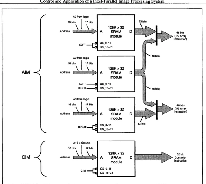
Figure 2-9 shows the old control store arrangement. Each memory module was 128K x 32 bits. The CIM used one module, and simply threw away 64K of memory space. Because the array instruction was 88 bits, a total of 96 bits were stored for each array instruction, 88 of which are used by the array, with the remaining eight being used as extra instruction bits for the controller. Rather than having 88 wires going from the controller to the array, the instructions were sent out in two 44-bit chunks. This was done by clocking the AIM reads twice as fast as the rest of the controller, sending half of the instruction each time. Address bit A0 in the AIM was used to do
the instruction selection, while the Left/Right chip selects were used to send either half of the 88 bits to the array. This arrangement added complexity and hardware to the 10 MHz controller's architecture. To program the AIM, two instructions had to be combined together, and divided into three 32-bit pieces to be loaded into the various modules. There were four host-controller inter-face functions (WRTAIMLO, WRTAIMRO, WRTAIML1, WRTAIMR1) used to write to the mem-ory.
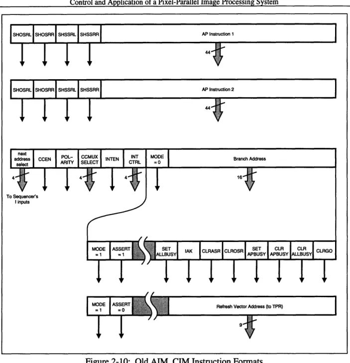
The new design uses three 64K x 32 SRAM SIMMs. One module is for the CIM, and two are for the AIM, for the instruction selection. All address and data lines are wired identically, the only difference being the chip selects for the two AIM modules come directly from the SSR's output bit. This simplified the hardware present on the board, the logic controlling chip select signals, and the programming of the control store. There are now only two host-controller functions used to write the memory, and memory programming takes less cycles than in the previous controller. The instruction format for the controller instructions was also significantly simplified. Figure 2-10 shows the CIM and AIM words for the old controller, and Figure 2-11 for the new controller. The software framework provided the controller instruction assembler, to translate from the high-level control instructions into the actual bits of the CIM word. To maintain software compatibil-ity, the interface to the assembler was kept the same, and the assembler itself was changed to pro-duce the new bits. For instance, an old instruction such as "next (shssrl shosrr)" now assembles to
Control and Application of a Pixel-Parallel Image Processing System
Figure 2-9: 10 MHz Controller Control Store
produce active bits (SSRCE, SHSSRL, OSRCE), rather than (SHSSRL, SHOSRR). There were many ways such as this to take advantage of the software interface in order to make the hardware more efficient without impacting the existing application programmer's interface. The reason for this particular change, in the SSR and OSR signals, lies in the way shift registers are implemented internally in the EPLDs.
Other changes are more obvious. A bit was eliminated by consolidating SETALLBUSY, CLRALLBUSY, SETAPBUSY, CLRAPBUSY into SETCLR, AP, ALL. This makes it impossi-ble to, for instance, set ALLBUSY and clear APBUSY in the same cycle, but this capability is never required. Another change is that the GO bit is now cleared by hardware when a sequence is launched, removing the CLRGO bit. The interrupt logic is now entirely hardware controlled, removing the need for the IAK bit. Removing priority interrupts got rid of four INTCTRL bits. And simplifying the interrupt vector address generation removed the need for the 9-bit refresh vector address field. With these modifications, the control instruction is able to fit into the 32-bit CIM, without the need for the MODE or ASSERT bits changing the function of various bits
Control and Application of a Pixel-Parallel Image Processing System
next
address CCEN PRIT SELC INTEN TC L
4
44
4 f To Sequencer's I inputs MODE RT =1J
MODE Branch Address
-= 0 1
ISE
ISY
ICLR C CLRGO_A RS , APBUSVI APBUSYu'
I
CGOFigure 2-10: Old AIM, CIM Instruction Formats
(which significantly complicates instruction decoding). However, to accomplish this, the new controller uses five bits in the AIM for control instructions, where the old controller used four. This is acceptable, as the HDPP chips need only 27 bits for each instruction.
2.2.7
Memory Refresh Interrupt
As mentioned, the previous controller had hardware support for four levels of priority interrupts, which could be interrupted by higher-priority interrupts. This hardware was developed with no clear purpose in mind, and in the final system, was not used at all. In fact, the only real use for interrupts would have been to refresh the DRAM cells in the array, but even here, the interrupts were not tested or used -- instead, memory refresh sequences were embedded in the application explicitly by the programmer.
I
Control and Application of a Pixel-Parallel Image Processing System
Figure 2-11: New AIM, CIM Instruction Formats
The final system has as a goal, as complete a separation between the hardware and the program-mer as possible. One aspect of this is removing the need to know about the refresh requirements of the array being used. Therefore, a requirement for an interrupt for use in memory refresh was
added to this controller, as well as built-in implementation of this interrupt.
This dictated the need for only a single interrupt, so priorities were eliminated. However, because the memory on the HDPP chips has not yet been characterized, there is a need for greater flexibil-ity in the refresh interval. In addition, it is also desirable to have some method of specifying in
software where the refresh sequence will be, as opposed to hard-coding the location.
A requirement for refresh intervals varying from 100 us to 500 ms was set, to cover all possible refresh intervals needed by the array. Because it was impossible to generate this much resolution in a 16-bit counter without adding several clock dividers, a new CCR architecture was developed. The 16-bit CCR is used to load the upper 16 bits of a 24-bit counter. The lower 8 bits are reset when starting the refresh count. This gives the capability of a count ranging from 256 to 16,776,960. Assuming a 20 MHz clock, this equates to refresh intervals from 12.8 us to .839 s. In addition, the framework now initializes this counter to set a refresh interval of 100 ms (assum-ing a 20 MHz clock), load(assum-ing the 16-bit CCR with hexadecimal 1E85 (decimal 7813).
The generation of the interrupt vector was also changed. In the old controller, an additional regis-ter (TPR) was used to hold an inregis-terrupt address. There was a specifically formatted CIM instruc-tion for programming this register, that didn't use the host-controller interface (see Figure 2-10). This register would then point to the memory location containing the interrupt service routine (ISR).
In the new controller, logic more similar to general-purpose computers is used. An address is hard-wired on the controller board, pointing to an interrupt vector table. In this case, the table has
next
select ARITY ISELECT CLR AP ALL CLRPS CLROSR MAP Branch Address
4 4 16
To Sequencer's I inputs
Control and Application of a Pixel-Parallel Image Processing System
only one entry, but the idea is the same. When an interrupt occurs, the register's contents are sup-plied to the memory, and the current address is placed on the stack. At this memory location resides the interrupt vector, which is simply a branch to wherever in memory the ISR resides. In this way, the table may be placed in a small portion of reserved memory, but the larger ISRs may be placed anywhere in memory, and moved around at run time. At the end of each ISR, then, is the return that pops the stack and continues program flow.
Control and Application of a Pixel-Parallel Image Processing System
Chapter 3
New Controller Requirements
The previous controller had a number of issues that motivated this research. These issues were as follows:
Decreasing board size -the new system is targeted to fit into a VME chassis on a workbench.
This is to enable this system to be portable and somewhat more sturdy. Because the previous con-troller was done using wire-wrap techniques and a large number of PLDs, there are ample oppor-tunities to optimize the size of the board itself.
Increasing system speed -the previous controller was to deliver complete instructions to the array
at a frequency of 10 MHz. This figure was chosen because it was estimated that this would be close to the maximum speed at which the array could operate. The new processor in this system is expected to have a higher clock frequency, and thus the controller must have a corresponding increase in speed. The new controller is capable of delivering instructions at 20 MHz.
Increasing controller robustness -a wire-wrap board, while suitable for fast prototyping and
test-ing, is not a robust method for a portable system that is intended to operate for any long period of time. In addition to this shortcoming, the previous controller wouldn't function at a clock period of 100 ns or lower (the target), and fell into and out of stability at certain lower clock periods. The new design investigated this problem and implemented changes.
3.1 Decreasing Board Size
3.1.1
PCB Technology
As mentioned, one of the primary goals of this thesis was to achieve greater logic integration on the controller board, in order to have a system that will fit cleanly into a standard VME chassis. One way to achieve this goal was to make this controller a printed circuit board. This, along with using surface-mount ICs as much as possible, greatly reduced board area. This was due to the fact that not only were modem surface-mount ICs available with much smaller footprints than equiva-lent DIP packages, but the newer parts were also more integrated. For instance, register chips included twice as many registers as before.
Not all devices were available in surface-mount packages, however. Notably, the microprogram sequencer in a DIP package was retained on the new controller. This was due to the fact that other packages were not readily available, and too much work in the software application framework was built around the sequencer's architecture to change to a microprocessor-based controller.
Control and Application of a Pixel-Parallel Image Processing System
3.1.2
Logic Integration
Another strategy was to integrate as much of the logic as possible into Xilinx programmable logic devices. The decision to use Xilinx was made primarily for economic reasons: previous research in this lab has been done with Xilinx products, so the software tools were already owned and installed.
Xilinx offered two suitable types of programmable logic devices: Field Programmable Gate Arrays (FPGAs), and Erasable Programmable Logic Devices (EPLDs). Each offers distinct advantages and disadvantages to different types of applications. EPLDs are suitable for complex controllers, high speed state machines, wide decoders, and PAL-integration. FPGAs have key applications as simple state machines, complex logic replacement, and board integration [9]. As the previous controller board consisted of 29 PALs (primarily 22V10s), EPLDs would make combining these devices a simpler task than with FPGAs, simply because the design software (at the time this research was begun) supported ABEL-style design files with EPLDs, but not with FPGAs. However, FPGAs allow much more integration of SSI logic, such as registers, and are capable of more complex logic internally. EPLDs have predictable timing paths and guarantee 100% routability and use of resources, while FPGAs have variable timing based on routing, and will not allow use of all internal resources due to routing limitations.
As the critical path analysis in Section 3.2.2 will show, only 15 ns of overhead was finally avail-able in the 50 ns clock period, to resolve several 13-input 1-output registered equations. Xilinx FPGAs are made up of a dense array of Configurable Logic Blocks (CLBs) which allow any type of logic to be implemented using basic lookup tables. Figure 3-1 shows the structure of a Config-urable Logic Block in a Xilinx FPGA. Each CLB receives eight inputs from the I/O blocks. These can each be used to generate two outputs based on four inputs each, or can be combined in the H logic block, to generate an output based on nine inputs. Xilinx specifies the delay through each CLB (via the H' path) as 7.0 ns (this is based on the fastest version of the 4000H family, which is high I/O). To implement the 13 input equation, a minimum of two CLBs would be nec-essary. Taking into account routing delays (which are significant and unpredictable in FPGAs)
and I/O delays, the worst-case critical path using this FPGA would exceed 50 ns.
Figure 3-2 shows the basic design of a Xilinx X7300 family EPLD (more or less function blocks are present depending on which EPLD is chosen). Each Fast Function Block (FFB) receives a total of 24 inputs, from the Fast Input block and from the Universal Interconnect Matrix (UIM). Each FFB contains nine "macrocells", and each of these can implement five product terms with 24 inputs, with a total block delay of 7.0 ns. Therefore the critical path equation can be done with a single FFB, yielding the resultant critical path that is under 50 ns (refer to Section 3.2 for this calculation).
3.1.3
Logic Modification
In addition to increased logic integration, effort was taken to redesign any portions of logic that could be further reduced to save resources. One of the first ways of doing this was taking advan-tage of the new HDPP architecture, which only requires 27 bits per instruction (compared to the
Control and Application of a Pixel-Parallel Image Processing System
Figure 3-1: FPGA CLB Architecture
CAPP, which required 88 bits). This saves in several areas -- less registers were required to latch and read or write these instructions to the AIM or the array. In addition, the AIM could be con-structed with two 64K x 32 SRAMs, rather than three, as was the case in the previous controller. This had other side effects of reduced memory-interface logic in the EPLDs, as well.
Another place where logic was saved was the Interrupt Control portion of the controller. The pre-vious controller employed a sophisticated and complicated interrupt controller. It was capable of four levels of interrupts, the highest priority of which was used for memory refresh. It also sup-ported nested interrupts, and maskable interrupts. However, in practice, this interrupt controller was never tested or used in the CAPPs image processing system. Instead, memory refresh sequences were explicitly added to application code by the programmer.
It was desired to completely hide the memory refresh from application writers in the final design, so this solution was not acceptable. In the interests of making the controller as simple as possible, though, it was decided not to have an interrupt capability comparable to that of a complete desk-top computer. Instead, support for a single interrupt for use as memory refresh only, was added to the new design. The previous design used five PAL22VO10s for the interrupt logic, and two more for the CCR refresh counter. By eliminating much of this logic, the counter is still present, but the five PALs were reduced to the equivalent of three (three function blocks in one EPLD).
Control and Application of a Pixel-Parallel Image Processing System
Figure 3-2: EPLD (XC7300) Device Block Diagram
3.1.4
Results of Integration/Modification
The final results of these efforts to reduce board size were successful. Table 3-1 shows a compar-ison of the final parts used on the old and the new controllers. Clearly, the largest savings were in