HAL Id: tel-01104855
https://hal.archives-ouvertes.fr/tel-01104855
Submitted on 19 Jan 2015HAL is a multi-disciplinary open access archive for the deposit and dissemination of sci-entific research documents, whether they are pub-lished or not. The documents may come from teaching and research institutions in France or abroad, or from public or private research centers.
L’archive ouverte pluridisciplinaire HAL, est destinée au dépôt et à la diffusion de documents scientifiques de niveau recherche, publiés ou non, émanant des établissements d’enseignement et de recherche français ou étrangers, des laboratoires publics ou privés.
Public Domain
wireless autonomousdevices
Yuwei Zhou
To cite this version:
Yuwei Zhou. Contribution to electromagnetic energy harvesting for wireless autonomousdevices. En-gineering Sciences [physics]. UNIVERSITE DE NANTES, 2013. English. �NNT : ED503-203�. �tel-01104855�
Thèse de Doctorat
Yuwei ZHOU
Mémoire présenté en vue de l’obtention
du grade de Docteur de l’Université de Nantes
Sous le label de l’Université Nantes Angers Le Mans
Discipline : Electronique
Spécialité : Télécommunications Laboratoire : IETR UMR 6164
Soutenance le 31 octobre 2013
École doctorale Sciences et Technologies de l’Information et Mathématiques (STIM) Thèse N° ED503-203
Contribution à la récupération
de l’énergie électromagnétique ambiante
pour les objets communicants autonomes
JURY
Président : M. Benoit GUIFFARD, Professeur, Faculté des Sciences et Techniques, Université de Nantes
Rapporteurs : M. Jean Lou DUBARD, Professeur, Université de Nice Sophia Antipolis M. Fabien NDAGIJIMANA, Professeur, INPG Grenoble
Examinateurs : M. Eduardo MOTTA-CRUZ, Ingénieur/HDR, Bouygues Telecom, Nantes
Directeur de Thèse : M. Tchanguiz RAZBAN, Professeur, Ecole polytechnique de l’université de Nantes
Co-encadrant : M. Bruno FROPPIER, Maître de Conférences, IUT de la Roche s/Yon
Acknowledgements
One of the joys of completion is to look over the journey past and remember all the professors, friends, and family who have helped and supported me along this long but fulfilling road.
I would like to express my heartfelt gratitude to my supervisors, Professor Tchanguiz RAZBAN and Professor Bruno FROPPIER, for providing me with the opportunity to complete my PhD thesis at the University of Nantes. They are not only mentors but dear friends. They have been actively interested in my work and have always been available to advise me. I am grateful for their encourage-ment, patience, motivation, enthusiasm, and immense knowledge in the field of microwave passive components and RF circuit design, antennas and propagation, and their applications in wireless communications.
I also would like to thank the members of my PhD committee, Professor Jean Lou DUBARD, Professor Fabien NDAGIJIMANA, Professor Benoit GUIFFARD, and Professor Eduardo MOTTA-CRUZ, who have provided encouraging and con-structive feedback. It is not a easy task to review a thesis. I am grateful for helping to shape and guide the direction of the work with their thoughtful and instructive comments.
For this thesis, some layout realisation and experiments are essential. I grate-fully acknowledge the assistance of many colleagues at IETR and Polytech’ Nantes, especially Guillaume LIRZIN and Marc BRUNET, for the fabrication and mea-surements.
In the process of layout design and modelization, I met some problems about circuit simulation. I sent my questions to Agilent EEsof EDA and received their valuable responses. So I thanks to the engineers in the department of Technical Support Engineer and Trainer, Franz KUSIDLO and Haim SPIEGEL, for offering suggestions on works in progress and their generous support.
I am thankful to my friends in the University of Nantes for all the great times that we have shared. And I would like to thank my old friends in China for the happiest memories in the past.
This last word of acknowledgement I have saved is for my family because of their love, support, and sacrifices. Without their selfless dedication, I would not
have been living a life in France. Owing to the studying experience abroad, I am on the way to make my dream come true.
Contents
Acknowledgements i
List of Figures vii
List of Tables xv
1 Introduction 1
1.1 Background of energy harvesting . . . 1
1.1.1 Thermoelectric generator . . . 2
1.1.2 Mechanical resonator . . . 2
1.1.3 Photovoltaic cell . . . 3
1.1.4 RF sensor . . . 3
1.1.5 Implantable or wearable sensor . . . 3
1.2 Motivation . . . 4
1.3 Preliminary analysis of rectifying process . . . 6
1.3.1 Rectifying principle . . . 7
1.3.2 Diode model . . . 12
1.3.3 Impact of diode parameters . . . 20
2 State of The Art 29 2.1 Configuration of rectennas . . . 29
2.2 From series diode rectifier to bridge rectifier . . . 31
2.3 Compact bridge rectifier with no via-hole connection . . . 32
2.4 Dual-diode rectenna with harmonic-rejecting design . . . 34
2.5 Stacked rectenna with radial stubs . . . 35
2.6 Circularly polarized rectenna with unbalanced circular slots. . . 37
2.7 Harmonic-rejecting circular-sector rectenna . . . 38
2.8 Rectifier with high Q resonators . . . 39
2.9 Spiral rectenna for surrounding energy harvesting . . . 40
2.10 Dual-frequency for energy harvesting at low power levels . . . 41
2.11 Conclusion of the art state . . . 42
3 RF/DC Conversion 45 iii
3.1 Power range . . . 45
3.2 Design for high power levels . . . 47
3.2.1 Choice of the diode . . . 47
3.2.2 Choice of the load. . . 47
3.2.3 Realisation and measurement . . . 49
3.2.4 Analysis of matching circuits. . . 51
3.2.5 Sensitivity of the matching circuit . . . 55
3.3 Design for low power levels . . . 58
3.3.1 Choice of the diode and the load . . . 58
3.3.2 Design of matching circuits . . . 59
3.3.3 Comparison among different circuits . . . 65
3.3.4 Investigation in the simulation model . . . 67
3.4 Research to increase the efficiency . . . 71
3.4.1 Choice of lumped components . . . 71
3.4.2 Layout and realisation . . . 72
3.4.3 DC voltage and conversion efficiency . . . 73
3.5 Power management . . . 75
3.5.1 DC modelization . . . 75
3.5.2 MPPT . . . 79
3.6 Conclusion of the design of rectifying circuit . . . 80
4 Antenna Design for Energy Harvesting 83 4.1 Characteristics of antennas . . . 83
4.1.1 Microwave transmission equation . . . 83
4.1.2 Emitting antenna . . . 85
4.1.3 Description of the received power . . . 88
4.2 Patch antenna . . . 90
4.2.1 Dimension of the patch . . . 91
4.2.2 Impedance of the patch. . . 93
4.2.3 Frequency response of the patch . . . 95
4.2.4 Radiation patterns and gain . . . 95
4.3 Monopole antenna . . . 98
4.3.1 Prototype of the monopole . . . 99
4.3.2 Frequency response of the monopole . . . 100
4.3.3 Radiation patterns and gain . . . 101
4.4 Monopole with a shorting pin . . . 103
4.4.1 Prototype of the modified monopole. . . 104
4.4.2 Frequency response of the modified monopole . . . 105
4.4.3 Radiation patterns and gain . . . 105
4.4.4 Analysis of the received power . . . 108
4.5 Conclusion of the antenna design . . . 110
5 Combination and Integration of Rectenna 113 5.1 Design for high power levels . . . 113
Contents v
5.1.1 Rectenna experiment . . . 113
5.1.2 Rectifying circuit with HSMS-2820 . . . 114
5.2 Design for low power levels . . . 117
5.2.1 Rectifying circuit with HSMS-2860 . . . 117
5.2.2 Measurement in an anechoic chamber . . . 118
5.3 Rectenna integration . . . 121
5.3.1 Integrated monopole rectenna: rectenna I. . . 122
5.3.2 Integration of DC loop: rectenna II . . . 123
5.3.3 Anechoic chamber experiment . . . 124
5.4 Rectenna with high efficiency . . . 127
5.4.1 Rectifying circuit with HSMS-2850 . . . 128
5.4.2 Integrated rectenna with HSMS-2850: rectenna III . . . 129
5.4.3 Integrated rectenna with new DC loop: rectenna IV . . . 130
5.4.4 DC voltage and equivalent efficiency . . . 131
5.5 Conclusion of rectenna design . . . 134
6 Conclusion and Perspective 137 6.1 Conclusion . . . 137
6.2 Perspective . . . 140
Bibliography 143
List of Figures
1.1 Schematic of the power harvesting system . . . 1
1.2 Equivalent model of Schottky diode without parasitic package . . . 7
1.3 Half-wave rectification . . . 10
1.4 Scheme of a rectifying circuit . . . 10
1.5 Prototype of a rectifying circuit with single serial diode . . . 11
1.6 Cross-section of Schottky diode . . . 12
1.7 Equivalent circuit model of diode chip . . . 12
1.8 Metal-semiconductor junction . . . 13
1.9 DC simulation of diode models . . . 17
1.10 Comparison of diode models in DC simulation . . . 17
1.11 Schematic current-voltage characteristic of Schottky diode HSMS-2860 . . . 18
1.12 S-parameter simulation of diode models: (a)Vendor model; (b)SPICE model; (c)SPICE model with package parasitics . . . 19
1.13 Comparison of diode models in S-parameter simulation . . . 19
1.14 Schematic of the simulated model considering zero-bias junction capacitance . . . 20
1.15 Efficiency comparison in terms of zero-bias junction capacitance . . 21
1.16 Schematic of the simulated model considering series ohmic resistance 22 1.17 Efficiency comparison in terms of series ohmic resistance . . . 22
1.18 Efficiency comparison in terms of saturation current . . . 23
1.19 Efficiency comparison in terms of junction potential . . . 23
1.20 Efficiency comparison in terms of emission coefficient . . . 24
1.21 Efficiency comparison in terms of grading coefficient . . . 24
1.22 Efficiency comparison in terms of breakdown voltage . . . 25
1.23 Efficiency comparison among Schottky diode 2810, HSMS-2820, HSMS-2850, and HSMS-2860 . . . 25
2.1 Topologies of rectennas . . . 30
2.2 Serial and bridge rectifiers designed by H. Takhedmit . . . 31
2.3 Compact bridge rectifier designed by H. Takhedmit . . . 32
2.4 Impedance schema of diodes D1-D4 . . . 33
2.5 Geometry of dual-diode rectenna (dimensions in mm) designed by H. Takhedmit . . . 34
2.6 Layout of the stacked rectenna designed by J. A. G. Akkermans . . 36 vii
2.7 Antenna and rectifying circuit configuration and the photographs of proposed rectenna designed by T. C. Yo. Geometry parameters for the CP antenna are: W=60, L=60, Rp=15.5, Fr=6.5, d1=5.2,
r1=5.2, d2=8.3, r2=2.3, h1=1.6, h1=0.8 (Dimension:mm) . . . 37
2.8 Schematic and photograph of doubler rectifier with 3rd harmonic rejection radial stub designed by T. C. Yo . . . 38
2.9 Rectenna with a microstrip circular-sector antenna designed by J. Y. Park . . . 39
2.10 Equivalent circuit with 24 MHz crystal resonator QCand two
HSMS-286x diodes from Agilent for the rectification, designed by T. Ungan 39
2.11 Rectenna prototype with spiral antenna designed by D. Bouchouicha 40
2.12 Dual-frequency rectenna designed by Z. Saddi . . . 41
3.1 Series diode circuit with matching circuit . . . 45
3.2 S parameters and efficiencies for given designs of different power levels 46
3.3 Effective efficiency versus the transmitted power in terms of load resistance . . . 48
3.4 Input impedance of 10 dBm design versus the transmitted power. . 48
3.5 Configuration of a rectifying circuit designed for 10 dBm . . . 49
3.6 Frequency response of a rectifying circuit designed for 10 dBm . . . 49
3.7 DC output voltage of 10 dBm design versus the input power . . . . 50
3.8 Conversion efficiency of 10 dBm design versus the input power . . . 50
3.9 Scheme of single stub matching circuit . . . 52
3.10 Frequency response of circuits with single stub matched for 10 dBm 52
3.11 Power response of circuits with single stub matched at 2.45 GHz . . 52
3.12 S parameter variation of the design with single stub matching circuit 53
3.13 Scheme of tapered line matching circuit . . . 53
3.14 Frequency response of circuits with tapered line matched for 10 dBm 54
3.15 Power response of circuits with tapered line matched at 2.45 GHz . 54
3.16 S parameter variation of the design with tapered line matching circuit 54
3.17 Fabricated rectifying circuits with some different details . . . 55
3.18 Frequency response simulated (red curve) and measured (blue curve) with more precise layouts. . . 56
3.19 Measured output DC voltage of 10 dBm design for precise layout . 57
3.20 Measured conversion efficiency of 10 dBm design for precise layout . 57
3.21 design 1 : rectifying circuit with single stub matching circuit . . . . 59
3.22 Return loss of a rectifying circuit with single stub . . . 60
3.23 Measured DC voltage of rectifying circuits with single stub: design 1 forward diode (cyan curve); design 1r reverse diode (magenta curve) 60
3.24 Measured conversion efficiency of rectifying circuits with single stub: design 1 forward diode (cyan curve); design 1r reverse diode (ma-genta curve) . . . 61
3.25 design 2 : rectifying circuit with radial stubs low pass filter . . . 61
List of Figures ix
3.27 Measured DC voltage of rectifying circuits with radial stubs low pass filter: design 2 forward diode (black curve); design 2r reverse
diode (red curve) . . . 63
3.28 Measured conversion efficiency of rectifying circuits with single stub: design 2 forward diode (black curve); design 2r reverse diode (red curve) . . . 63
3.29 design 3 : rectifying circuit with compact structure . . . 64
3.30 Return loss of a rectifying circuit with compact structure . . . 64
3.31 Measured DC voltage of rectifying circuits with compact structure: design 3 forward diode (green curve); design 3r reverse diode (blue curve) . . . 65
3.32 Measured conversion efficiency of rectifying circuits with compact structure: design 3 forward diode (green curve); design 3r reverse diode (blue curve). . . 65
3.33 DC voltage comparison of rectifying circuit configurations. . . 66
3.34 Efficiency comparison of rectifying circuit configurations . . . 66
3.35 Configuration of a rectifying circuit designed for -20 dBm . . . 68
3.36 Post-simulated and measured return loss of the rectifying circuit designed for -20 dBm against the frequency. . . 69
3.37 Post-simulated and measured return loss of the rectifying circuit designed for -20 dBm against the input power . . . 69
3.38 Post-simulated and measured DC output voltage of the rectifying circuit . . . 70
3.39 Post-simulated and measured conversion efficiency of the rectifying circuit . . . 70
3.40 Configuration of a rectifying circuit with HSMS-2850 . . . 72
3.41 Simulated and measured frequency response of the rectifying circuit with HSMS-2850 . . . 72
3.42 Simulated and measured DC voltage of the rectifying circuit with HSMS-2850 . . . 73
3.43 Simulated and measured conversion efficiency of the rectifying cir-cuit with HSMS-2850 . . . 74
3.44 Simulated conversion efficiency of the rectifying circuit with HSMS-2850 against the length of L3 . . . 74
3.45 Simulated conversion efficiency of the rectifying circuit with HSMS-2850 against the load . . . 75
3.46 Single serial diode configuration of rectifying circuits . . . 75
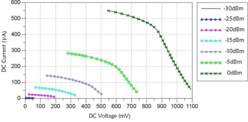
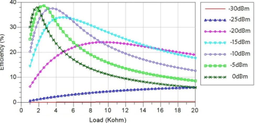
3.47 Simulated DC current-voltage curves of diodes HSMS-2860 for dif-ferent power levels . . . 76
3.48 Simulated efficiencies of diodes HSMS-2860 in terms of load resis-tances for different power levels . . . 77
3.49 Simulated DC current-voltage curves of diodes HSMS-2850 for dif-ferent power levels . . . 78
3.50 Simulated efficiencies of diodes HSMS-2850 in terms of load resis-tances for different power levels . . . 78
4.1 Experimental set-up of an antenna . . . 83
4.2 Scheme of antenna measurements . . . 84
4.3 Emitting horn antenna . . . 85
4.4 Measured gain of the emitting horn antenna . . . 87
4.5 Power density versus range . . . 90
4.6 Microstrip patch antenna . . . 91
4.7 Top view of patch antenna . . . 92
4.8 Equivalent circuit of rectangular patch antenna . . . 93
4.9 Configuration of the patch . . . 94
4.10 Simulated and measured return loss of the patch . . . 95
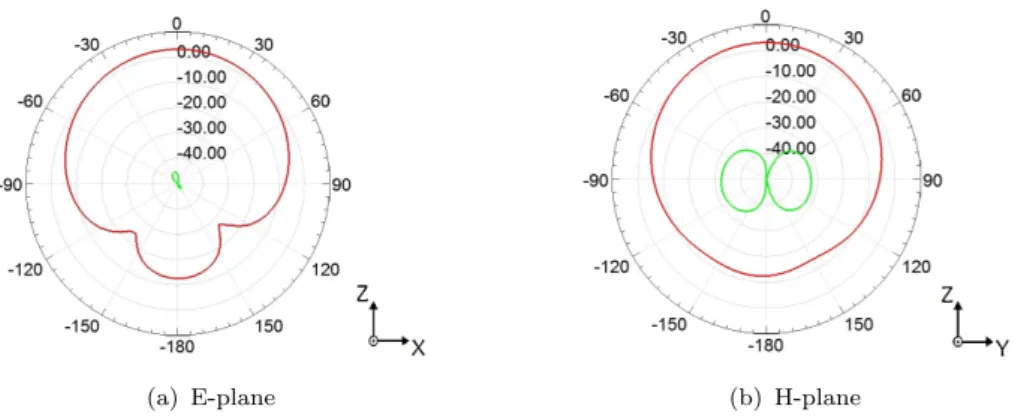
4.11 Simulated radiation patterns of E-plane and H-plane in co-polarization (red line) and cross-polarization (green line) of the patch . . . 96
4.12 Measured radiation patterns of E-plane and H-plane in co-polarization (red line) and cross-polarization (green line) of the patch . . . 96
4.13 Radiation patterns of the patch with frequency sweep . . . 97
4.14 Simulated 3D gain of the patch . . . 98
4.15 Configuration of the monopole . . . 99
4.16 Simulated and measured return loss of the monopole . . . 100
4.17 Simulated (red line) and measured (blue line) radiation patterns of the monopole . . . 101
4.18 Radiation patterns of the monopole with frequency sweep . . . 102
4.19 Measured gain of the monopole . . . 103
4.20 Simulated 3D gain of the monopole . . . 103
4.21 Configuration of the monopole with a shorting pin . . . 104
4.22 Simulated and measured return loss of the monopole with a shorting pin . . . 105
4.23 Simulated (red line) and measured (blue line) radiation patterns of the monopole with a shorting pin . . . 106
4.24 Radiation patterns of the modified monopole with frequency sweep 107 4.25 Measured gain of the monopole with a shorting pin . . . 107
4.26 Simulated 3D gain of the monopole with a shorting pin . . . 108
4.27 Measured received power of the monopole with a shorting pin against the frequency . . . 109
4.28 Measured received power of the monopole with a shorting pin against the rotation angle . . . 109
5.1 Rectenna experiment set-up with a movable position . . . 113
5.2 Modified rectifying circuit with a patch antenna . . . 115
5.3 Output DC voltage of the rectenna integrated with a patch . . . 115
5.4 Conversion efficiency of the rectenna integrated with a patch . . . . 116
5.5 Output DC voltage of the rectenna integrated with a patch against power densities . . . 116
5.6 Conversion efficiency of the rectenna integrated with a patch against power densities . . . 117
List of Figures xi
5.8 Antenna shelf . . . 119
5.9 Vout comparison between the rectifying circuit and the circuit with the monopole . . . 119
5.10 Efficiency comparison between the rectifying circuit and the circuit with the monopole . . . 120
5.11 Output DC voltage of the rectifying circuit with the antenna against the rotation angle . . . 121
5.12 Conversion efficiency of the rectifying circuit with the antenna against the rotation angle . . . 121
5.13 Configuration of the rectenna I . . . 122
5.14 Configuration of the rectenna II . . . 124
5.15 Experimental set-up of a rectenna . . . 124
5.16 Measured DC voltage of the rectennas I and II against the power density at 0◦ . . . 125
5.17 Equivalent efficiency of the rectennas I and II against the power density at 0◦ . . . 125
5.18 Measured DC voltage of the rectennas I and II against the power density at -90◦ . . . 126
5.19 Equivalent efficiency of the rectennas I and II against the power density at -90◦ . . . 127
5.20 Rectifying circuit with HSMS-2850 connected with the modified monopole . . . 128
5.21 Configuration of the rectenna III . . . 129
5.22 Configuration of the rectenna IV . . . 130
5.23 Measured DC voltage of the rectennas III and IV against the power density at 0◦ . . . 131
5.24 Equivalent efficiency of the rectennas III and IV against the power density at 0◦ . . . 132
5.25 Equivalent efficiency of the rectennas III and IV against the incident power at 0◦ . . . 132
5.26 Measured DC voltage of the rectennas III and IV against the rota-tion angle . . . 133
5.27 Equivalent efficiency of the rectennas III and IV against the rotation angle . . . 133
6.1 Conversion efficiency of rectifying circuits in Epoxy and in Arlon . . 140
6.2 Conversion efficiency of circuits in Epoxy and in Arlon against the equivalent power density with 3 dBi antenna . . . 140
6.3 Sch´ema du syst`eme de r´ecup´eration d’´energie. . . 155
6.4 Mod`ele ´electrique d’une diode Schottky avec les ´el´ements parasites du boˆıtier . . . 158
6.5 Sch´ema d’un circuit de redressement . . . 161
6.6 Sch´ema d’un circuit redresseur de diode s´erie . . . 162
6.8 S11 en fonction de la fr´equence pour la conception de niveaux de
puissance ´elev´es . . . 164
6.9 Tension DC de sortie pour la conception de niveaux de puissance ´elev´es . . . 165
6.10 Rendement mesur´e et simul´e pour la conception de niveaux de puis-sance ´elev´es . . . 165
6.11 Circuit de redressement pour la conception de faibles niveaux de puissance . . . 166
6.12 S11en fonction de la fr´equence pour la conception de faibles niveaux de puissance . . . 167
6.13 S11en fonction de la puissance pour la conception de faibles niveaux de puissance . . . 168
6.14 Tension DC de sortie pour la conception de faibles niveaux de puis-sance . . . 168
6.15 Rendement mesur´e et simul´e pour la conception de faibles niveaux de puissance . . . 169
6.16 Circuit de redressement pour la conception `a haute efficacit´e . . . . 170
6.17 S11 en fonction de la fr´equence pour la conception `a haute efficacit´e 171 6.18 Tension DC de sortie pour la conception `a haute efficacit´e . . . 171
6.19 Rendement mesur´e et simul´e pour la conception `a haute efficacit´e . 172 6.20 Rendement simul´e en fonction de la longueur L3 . . . 172
6.21 Rendement simul´e en fonction de la r´esistance de charge . . . 173
6.22 Antenne patch rectangulaire . . . 174
6.23 S11 en fonction de la fr´equence pour l’antenne patch . . . 174
6.24 Les diagrammes de rayonnement simul´es sur le plan E et sur le plan H en co-polarisation (courbe rouge) et en polarisation crois´ee (courbe verte) pour l’antenne patch . . . 175
6.25 Les diagrammes de rayonnement mesur´es dans le plan E et dans le plan H en co-polarisation (courbe rouge) et en polarisation crois´ee (courbe verte) pour l’antenne patch . . . 176
6.26 Les diagrammes de rayonnement en fonction de la fr´equence et de l’angle de rotation pour l’antenne patch. . . 176
6.27 Antenne monopˆole . . . 177
6.28 S11 simul´e et mesur´e d’antenne monopˆole . . . 178
6.29 Les diagrammes de rayonnement simul´es (courbe rouge) et mesur´es (courbe blue) d’antenne monopˆole . . . 178
6.30 Les diagrammes de rayonnement en fonction de la fr´equence et de l’angle de rotation pour l’antenne monopˆole . . . 179
6.31 Gain mesur´e de l’antenne monopˆole . . . 180
6.32 Antenne monopˆole court-circuit´ee . . . 180
6.33 S11 simul´e et mesur´e d’antenne monopˆole court-circuit´ee . . . 181
6.34 Les diagrammes de rayonnement simul´es (courbe rouge) et mesur´es (courbe blue) d’antenne monopˆole court-circuit´ee . . . 181
6.35 Les diagrammes de rayonnement en fonction de la fr´equence et de l’angle de rotation pour l’antenne monopˆole court-circuit´ee . . . 182
List of Figures xiii
6.36 Gain mesur´e de l’antenne monopˆole court-circuit´ee . . . 183
6.37 Rectenna pour des niveaux de puissance ´elev´es . . . 184
6.38 Montage exp´erimental de la rectenna avec une position mobile . . . 184
6.39 Tension DC de sortie de la rectenna pour les niveaux de puissance ´elev´es . . . 185
6.40 Rendement mesur´e et simul´e de la rectenna pour les niveaux de puissance ´elev´es . . . 185
6.41 Rectenna I pour les faibles niveaux de puissance . . . 186
6.42 Rectenna II pour les faibles niveaux de puissance . . . 187
6.43 Tension DC de sortie des rectennas I et II en fonction de la densit´e de puissance `a 0◦ . . . 188
6.44 Rendement ´equivalent des rectennas I et II en fonction de la densit´e de puissance `a 0◦ . . . 188
6.45 Tension DC de sortie des rectennas I et II en fonction de la densit´e de puissance `a -90◦ . . . 189
6.46 Rendement ´equivalent des rectennas I et II en fonction de la densit´e de puissance `a -90◦ . . . 190
6.47 Rectenna III `a haute efficacit´e . . . 190
6.48 Rectenna IV `a haute efficacit´e . . . 191
6.49 Tension DC de sortie des rectennas III et IV en fonction de la densit´e de puissance `a 0◦ . . . 192
6.50 Rendement ´equivalent des rectennas III et IV en fonction de la densit´e de puissance `a 0◦ . . . 193
6.51 Tension DC de sortie des rectennas III et IV en fonction de l’angle de rotation. . . 193
6.52 Rendement ´equivalent des rectennas III et IV en fonction de l’angle de rotation. . . 194
List of Tables
1.1 Typical parameters of Schottky diode HSMS-28xx . . . 26
1.2 Typical parameters of other Schottky diodes . . . 27
2.1 Reference of rectenna design . . . 43
3.1 Comparison of rectifying circuits designed for 10 dBm . . . 58
3.2 Comparison of rectifying circuits designed for -20 dBm . . . 67
4.1 IDPH-2018 specifications . . . 86
5.1 Measured results of rectenna design . . . 135
6.1 Comparison of rectenna designs . . . 139
6.2 Les param`etres typiques des diodes Schottky de la s´erie HSMS-28xx 160 6.3 Les r´esultats mesur´es des rectennas . . . 194
6.4 Comparaison des rectennas. . . 196
Dedicated to whom I love and who loves me, especially
my parents. . .
Chapter 1
Introduction
1.1
Background of energy harvesting
People have searched for some ways to obtain the energy from nature re-sources, such as thermal effect, mechanical vibration, photovoltaic cells, and
elec-tromagnetic energy receivers, as shown in Fig. 1.1. These methods have provided
efficient and practical solutions to consumer, industrial, and military needs.
Figure 1.1: Schematic of the power harvesting system
The search for new energy harvesting devices is driven by sensor networks and green communications. The autonomous sensors exchange their data cooperatively through the network to a main location thanks to the technology of energy self-sufficiency at the terminals. The energy harvesting is needed to increase the
life-time of the sensor and to minimize the energy impact of the communication [1,2].
1.1.1
Thermoelectric generator
Thermoelectric power generation presents many advantages including solid-state operation with no moving parts, long life-times, no emission of toxic gases,
and high reliability [3]. The drawbacks of existing thermoelectric generators are
low efficiency and large size. A new generation of nano-structured thermoelectric energy harvesters has been introduced by companies such as Micropelt offering the promise to greatly increase thermoelectric efficiency. As a result, there is new interest in the commercial field with automakers looking at thermoelectric as a replacement for alternators thereby improving fuel efficiency. In this scenario, the thermoelectric generator could be wrapped around a car’s exhaust pipe to harvest
the waste heat and produce electricity [4].
1.1.2
Mechanical resonator
Mechanical energy harvesting devices produce electricity from vibration,
me-chanical stress and strain of the surface sensor [5]. Mechanical vibrations cause the
mass component to move and oscillate. This kinetic energy can be converted into electrical energy via an electromagnetic field, such as the strain on a piezoelectric material. Most vibration-powered systems rely on resonance to work, which im-plies there is a peak frequency and the system derives most of its energy at this
frequency [6].
The main device in mechanical energy harvesting is the piezoelectric device. Piezoelectric energy harvesting converts mechanical energy to electrical energy
by straining a piezoelectric material [7]. Strain or deformation in a piezoelectric
material causes charge separation across the device, producing an electric field, and consequently a voltage drop proportional to the stress is applied. The oscillating system is typically a cantilever-beam structure with a mass at the unattached end of the lever, since it provides higher strain for a given input force. The voltage produced varies with time and strain, effectively producing an irregular AC signal. Piezoelectric energy conversion produces relatively higher voltage and power levels
than the electromagnetic system [8].
Apart from piezoelectric sensors, mechanical energy harvesting can rely on natural sources from the environment such as wind and water flow. At large scale, windmills and turbines are well documented and can operate near the maximum
Chapter 1. Introduction 3 theoretical power. This is not the case for miniature devices which operate at a
much higher speed [9].
1.1.3
Photovoltaic cell
Ambient light can be used by photovoltaic cells to produce electricity either indoors or outdoors. Photovoltaic energy conversion is considered to be a ma-ture integrated circuit-compatible technology with potentially long life-times and
higher output power levels than other energy-harvesting mechanisms [10].
Photo-voltaic cells are exploited across a wide range of size scales area and power levels. The challenge is to conform to small surface area and its output power which strongly depends on environmental conditions, for example, on varying light in-tensity. Additionally, for different indoor light source, different emission spectra
affect the conversion efficiency for a given apparent light level [11].
1.1.4
RF sensor
A large number of potential RF sources exist in metropolitan environments, such as broadcast radio and TV, mobile telephony, and wireless networks. It is beneficial to collect parts of these disparate sources and convert them into useful energy. The conversion of electromagnetic energy is based upon a special type of rectifying antenna which is used to directly convert microwave energy into DC electricity. This device can operate 24 hours per day and even in an embedded de-vice. A simple rectenna can be constructed from a Schottky diode placed between antennas and loads. In laboratory environments, rectennas are highly efficient for
converting microwave energy to DC electricity [12,13]. However, the energy levels
actually are so low that present electronic devices are difficult to be supplied [14].
1.1.5
Implantable or wearable sensor
The biological body moves and radiates heat continuously. For an instance, the human body at rest is emitting about 100 watts into the environment. It is possible to capture some of this energy by power wearable electronics. Two meth-ods include active and passive energy harvesting methmeth-ods. The active powering of
electronic devices takes place when the user of the electronic product is required to perform a specific task that they would not normally carry out. The passive powering of electronic devices harvests energy from everyday actions the user, such
as walking, breathing, body heat, blood pressure, and finger motion [15].
While energy harvesting from human body may be useful as a supplemental power source, the current research in this field tries to combine existing techniques to create more efficient power generators. A number of efforts have been funded to harvest energy from leg and arm motion, shoe impacts, blood pressure for low
level power, and implantable or wearable sensors [16,17]. The need is to improve
the energy generation capabilities of individual techniques.
1.2
Motivation
The technology of energy self-sufficiency has received an increasing attention
in the field of power supplying for wireless devices [18]. Rectennas (Rectifying
antennas) give a reliable way to increase the life-time of network sensors and to minimize the energy impact of wireless devices. A rectenna usually consists of a receiving antenna and a rectifying circuit. It is capable of capturing the microwave energy from surrounding environments and converting the electromagnetic energy into useful DC energy.
The existing designs of rectennas are mostly applicable with high conversion efficiency for high power levels at frequency bands of ISM (Industry, Scientific, and
Medical) or GSM (Global System for Mobile) [19]. These rectennas participate
in the application of microwave power transmission. First of all, DC electrical power is converted into RF power by power generators. The RF power is then transmitted through space to some distant point by antennas. Finally the power
is collected and converted into DC power at the receiving point by rectennas [20].
The overall efficiency of energy transmission system is necessarily the product of the individual efficiencies associated with the energy emitting, receiving, and converting processes of the system. The usability depends upon efficient conversion technology as well as upon aperture-to-aperture transfer efficiency. The modern free-space power transmission needs to achieve the combined objectives of high efficiency, low cost, high reliability, and low mass at the transmitting and receiving
Chapter 1. Introduction 5 For example, an efficient rectenna based on a dual Schottky diodes converter and harmonic-rejecting configuration at 2.45 GHz exhibits an efficiency of 83 % at
0.31 mW/cm2 [22]. Another design is a CP (Circularly Polarized) gain
high-efficiency rectenna array in a coplanar stripline circuit. Each antenna has CP gain of 11 dB and each rectenna element achieves RF-to-DC conversion efficiency of 81
% at 5.71 GHz [23].
However, high levels of power density are not available everywhere. In the field of power transmission from a base station, the attenuation of microwave energy is inevitable for a long distance. Besides, human activities exist at low power densities in respect of the health standard.
According to the ICNIRP (International Commission on Non-Ionizing
Radia-tion ProtecRadia-tion) exposure guidelines, power densities are limited to 0.45 mW/cm2
(41 V/m) at 900 MHz and 0.9 mW/cm2 (58 V/m) at 1.8 GHz for mobile phone
base station frequencies, and 1 mW/cm2 (61 V/m) at the microwave oven
fre-quency 2.45 GHz [24, 25]. Announced by WHO (World Health Organization),
typical maximum public exposure levels are 10 µW/cm2 (6 V/m) for TV and
ra-dio transmitters and for mobile phone base stations, 20 µW/cm2 for radars, and 50
µW/cm2 for microwave ovens [26]. The investigation of electric field in practical
cases is between 0.14 V/m (5.2 nW/cm2) and 3 V/m (2.4 µW/cm2) as shown in
the COPIC newsletters and articles [27].
Under this condition, the device of power harvesting for low power levels is restricted by the diode behaviour. For an instance, the rectifier with a high Q crystal quartz resonator can achieve DC voltage 1 V and conversion efficiency more than 22 % for the power level -30 dBm but at a medium wave frequency 24
MHz [28]. Another example is a spiral rectenna with conversion efficiency 0.7 %
at the power power density 3.55 nW/cm2 at 1.85 GHz [29]. All in all, the rectenna
design succeeds in high efficiency at high power densities and low efficiency for low power levels. With the research of power density in an ambient environment, we found that in the aim of increasing the life-time of wireless devices without a specific RF beam, a rectenna with splendid efficiency at low power densities is necessary.
In this thesis, we present a study of Schottky diode rectenna for RF energy harvesting systems. The radiating part is a narrowband patch antenna or a broad-band monopole antenna. Integrated with the antenna on a PCB (Printed Circuit
Board), rectifying circuits are proposed with single Schottky diode for RF-DC conversion. Matching circuits are optimised to improve the power at fundamental frequency transferring inside the diode and to reject harmonic signals. The param-eters which determine the rectenna performance have been simulated in Agilent ADS (Advanced Design System) and Ansoft HFSS (High Frequency Structure Simulator).
Our rectennas can be used in point-to-point power transmission of high energy levels and power supplying far away from centralized power sources. Besides, these rectennas are suitable for power harvesting from surrounding environments at ISM frequencies, such as Wi-Fi, Bluetooth, and ZigBee networks. Batteries of wireless devices are recharged by rectennas which captures RF energy from ambient radiation sources at low power densities.
1.3
Preliminary analysis of rectifying process
The rectenna was invented by W. C. Brown and has been used for various applications such as the microwave power helicopter and the receiving array for
solar power satellites [30, 31]. It is one of the most important components in
microwave power transmission system. The main objective of the rectenna design is to obtain high conversion efficiency. The first approach is to collect maximum RF power. The second one is to convert the captured energy into DC energy efficiently.
The key to improve RF-to-DC conversion efficiency is the rectifying circuit.
The typical circuit includes a Schottky diode [32, 33], an input matching circuit,
an output low pass filter, and a load resistor. The performance of the circuit is determined by the non-linear process of Schottky diodes, by the barrier losses, and
by the series resistance loss [34–36]. It is difficult to predict the rectenna system
optimized for the maximum conversion efficiency. Some theoretical methods have
been studied to analyse the converting process in the time domain [37] and in the
Chapter 1. Introduction 7
1.3.1
Rectifying principle
The non-linear behaviour of Schottky diodes is performed due to two elements
of the equivalent model, a junction resistance Rj and a junction capacitor Cd, as
presented in Fig. 1.2. These two elements are non-linear, so as the series resistance
Rs. But Rsis generally considered as linear resistance because of its small variation
under forward bias [38].
Figure 1.2: Equivalent model of Schottky diode without parasitic package
Cd is the functions of Vd which is the voltage at two ends of Rj.
Cd∝ V
−1/2
d (1.1)
Suppose that the component Vd is driven by a RF power generator in form of
a sinusoidal voltage and the phase shift is zero.
Vd= V0cos(ωt + ϕ)
ϕ=0
−→ Vd= V0cos(ωt) (1.2)
where V0 is the maximum value of the sinusoidal voltage.
The current Id, passing through the junction resistance Rj, is given as follows.
Id= Is(e
qVd
N kT − 1) (1.3)
where Is is the saturation current (typically 1×10⁻¹² A).
k is Boltzmann’s constant (1.38×10⁻²³ JK−1). T is the junction temperature in Kelvins.
N is the emission coefficient (typically between 1 and 2). It depends on the
fabrication process and semiconductor material. In many cases, it is assumed to be approximately equal to 1. The factor is added to account for imperfect junctions as observed in real transistors.
Suppose that N kTq is one constant value a, then the equation (1.3) is simplified.
Id= Is(eaVd− 1) (1.4)
The equation above is transformed by the Taylor series [39].
Id= aIsV0cos(ωt) + a2I sV02 2! cos 2 (ωt) + a 3I sV03 3! cos 3 (ωt) + a 4I sV04 4! cos 4 (ωt) + · · · (1.5)
Then the equation above is deformed by mathematical methods.
Id= a2I sV02 2 · 2! + 3 · a4I sV04 8 · 4! + (aIsV0+ 3 · a3I sV03 4 · 3! ) cos(ωt) + ( a2I sV02 2 · 2! + a4I sV04 2 · 4! )cos(2ωt) +a 3I sV03 4 · 3! cos(3ωt) + a4I sV04 8 · 4! cos(4ωt) · · · (1.6)
Chapter 1. Introduction 9 Id = a2IsV02 2 · 2! + 3 · a4IsV04 8 · 4! | {z } DC + (aIsV0+ a3IsV03 4 · 2! ) | {z } f1 cos(2πf t) + (a 2I sV02 2 · 2! + a4IsV04 2 · 4! ) | {z } f2=2f1 ·cos(2π · 2f t) + a 3I sV03 4! | {z } f3=3f1 cos(2π · 3f t) + a 4I sV04 8 · 4! | {z } f4=4f1 cos(2π · 4f t) · · · (1.7)
According to the spectrum analysis of currents and voltages through diodes, currents are distributed at DC, fundamental frequency, and harmonic frequencies. Suppose the thermal voltage kT /q is 26 mV at the room temperature, a
non-linearity coefficient equals 1, and V0is 1 V, then DC signal and the second harmonic
are dominant in the equation of Id. That is to say, the generation of harmonics
exists. In details, DC component is 34.07 % of the total current value. The first and second harmonics are 7.05 % and 45.31 % of the total current respectively. The third and fourth harmonics are 2.34 % and 11.24 % of the total current.
A good behaviour of RF/DC conversion is obtained if RF filters are used to block signals at the fundamental frequency and at high order harmonics from transmitting to the load. Harmonic signals can be reflected and rectified again
in a new conversion cycle [40]. The conversion efficiency increases consequently
owing to the rectification process of signals at the fundamental frequency as well as the harmonics.
The common scenario in AC-to-DC conversion is a rectifier with a large smoothing capacitor which acts as a reservoir. After a peak of output voltages, the capacitor supplies currents to a load till the capacitor voltage falls to the value of next half-cycle of rectified voltages. At that point, rectifiers turn on again and deliver currents to the reservoir till a peak voltage is reached again. If the time constant is large in comparison to the period of the AC waveform, then a reason-able accurate approximation can be made by assuming that the capacitor voltage falls linearly. A useful assumption can be made if the ripple is small compared with the DC voltage. Then the capacitor is discharging all the way from one peak
to the next [41,42].
As we can see in Fig. 1.3, the half-wave rectifier is a simple type of rectifying
forward-biased and lets the current through. When the AC input is negative, the diode is reverse-biased and the diode does not let any current through. With the help of a large capacitor, the rectifier output yields DC voltage.
(a) (b)
(c) (d)
(e) (f)
Figure 1.3: Half-wave rectification
Figure 1.4: Scheme of a rectifying circuit
Generally rectifying circuits are composed by diodes, resistive loads, input
band pass filter, and output low pass filter, as shown in Fig. 1.4. The input band
Chapter 1. Introduction 11 harmonics going through the load and locks harmonic signals to participate a new rectifying cycle. In respect of conjugate matching, impedance matching circuits should be designed between receiving antennas and rectifying circuits in order to avoid the mismatch loss.
Take a single serial diode configuration for instance, as shown in Fig. 1.5. Pin
is the output power from the sum of power sources. Pt is the power effectively
inside the diode. Pr is the reflected power at the diode input. PDC is the output
DC power.
Figure 1.5: Prototype of a rectifying circuit with single serial diode
The efficiency of the overall system, noted by the global efficiency, is defined
by the ratio of output DC power to input RF power [43].
η = PDC Pin × 100% = V 2 DC/RL Pin × 100% (1.8)
The efficiency of the rectifying circuit, noted by the effective efficiency, is
defined by the ration of output DC power to transmitted RF power [43].
ηef f = PDC Pt × 100% = V 2 DC/RL Pt × 100% (1.9)
The effective efficiency is defined by taking into account an input mismatch. It is estimated regardless of mismatching loss. If an input band pass filter is well designed, the incident power from power sources transfers totally to the diode of rectifying circuits. In this case, the global efficiency can be high, which is close to the effective efficiency. In return, the global efficiency may be low due to the mismatch between the input impedance of diodes and the output impedance of power supply devices.
1.3.2
Diode model
The analysis of frequency components through Schottky diodes gives a de-scription about the relationship between diode parameters and DC output. It proves that RF filters are needed for pure DC output and high conversion effi-ciency. Following the section of theoretical analysis, the physical prototype of Schottky diodes is depicted as well as the equivalent circuit model with parasitic packaged elements.
A Schottky diode consists of a metal-semiconductor barrier formed by
depo-sition of a metal layer on a semiconductor [44]. A common type, the passivated
diode, is shown in Fig. 1.6, along with its equivalent circuit in Fig. 1.7.
Figure 1.6: Cross-section of Schottky diode
Rs is the parasitic series resistance of the diode, the sum of the bond-wire and
lead-frame resistance, the resistance of the bulk layer of silicon, etc. RF energy
coupled into Rs is lost as heat. Thus it does not contribute to the rectified output
of the diode. Cd is the parasitic junction capacitance of the diode, controlled by
the thickness of the epitaxial layer and the diameter of the Schottky contact.
Figure 1.7: Equivalent circuit model of diode chip
The diode has a non-linear behaviour. As seen in Fig. 1.7, the characteristic
Chapter 1. Introduction 13
junction resistor Rj and the junction capacitor Cd. Id is the current passing
through the junction resistance Rj and Vd is the voltage at its two ends. Lp is the
parasitic inductance. Cp is the parasitic capacitance.
The equation (1.3) describes the exact current through a diode, in terms of
the voltage dropped across the junction, the temperature of the junction, and
several physical constants. Id is proportional to the saturation current Is. Is is
the thermionic current from metal to semiconductor. It is related to the barrier
height of the diode. Is and Rs determine the DC characteristic of diodes.
The concept of barrier height of diodes is considered for the design of
recti-fying circuits, as shown in Fig. 1.8 [45]. A low barrier height metal has a low
forward voltage drop and a large reverse leakage current. Conversely, a high bar-rier height metal has a large forward voltage drop and a small reverse leakage current. Therefore, it is desirable to have a Schottky diode which exhibits the for-ward characteristics of a low barrier height metal and the reverse characteristics of a high barrier height metal.
Figure 1.8: Metal-semiconductor junction
The thermal potential kT /q is about 26 mV at room temperature. Assuming
the emission coefficient of 1, the diode equation is simplified to the equation (1.10).
Id= Is(e(
Vd
The depletion layer is located between the metal and the semiconductor of Schottky diodes. The diode in reverse bias exhibits a depletion-layer capacitance, called a junction capacitance. The junction capacitance is proportional to the zero-bias junction capacitance, one of SPICE (Simulation Program with Integrated
Circuit Emphasis) parameters [46].
Cd = Cj0(1 −
Vd
Vj
)−M (1.11)
where Cj0 is the zero-bias junction capacitance (0.7 pF for HSMS-2820; 0.18 pF
for HSMS-2850 and HSMS-2860).
Vj is the junction potential (0.65 V for HSMS-2820 and HSMS-2860; 0.35 V for
HSMS-2850).
M is the grading coefficient (1/2 for an abrupt junction; 1/3 for a linearly graded junction).
Constructed by metal-semiconductor junction rather than P-N junction, Schot-tky diodes are characterized by fast switching time, low reverse-recovery time, low forward voltage drop, and low junction capacitance. The equivalent circuit model shows the junction capacitor parallel with the junction resistor. The distribution of electricity component depends on the impedances of this junction capacitor and the resistor. The diode with small junction capacitance converts much RF energy and thus has good rectifying performance.
Take the single diode configuration as an example. The conduction loss is
calculated in terms of the current and the series resistance. The equation (1.12)
indicates that the increment of Rs influences negatively the global efficiency of
the circuit because of the increment of the conduction loss [47]. T is a rectifying
period. Ploss = 1 T Z t0 T 2+t0 Rsi2d(t)dt (1.12)
In the application of rectifying circuits, fast switching time equates to high speed capability and lower forward voltage drop equates to less power dissipation
Chapter 1. Introduction 15 when conducting. Schottky diodes are well suited for high-frequency applications. Because the forward voltage is low, the reverse-recovery time is short, and the junction capacitance is small.
Based on Agilent ADS simulation approaches, such as SP (Scattering Param-eter), LSSP (Large Signal Scattering ParamParam-eter), HBS (Harmonic Balance Simu-lation), and multiple parameter sweeps, the simulated model is built by taking into account an input mismatch. SP is used to characterize a passive RF component and establish the small-signal characteristics of a device at a specific bias and tem-perature. HBS is a frequency-domain analysis technique for simulating distortion in non-linear circuits and systems. LSSP is performed on non-linear circuits and thus includes non-linear effects such as gain compression and variations in power levels.
Assuming that all the power from energy sources participates in the rectifica-tion process, the global efficiency is close to the effective efficiency which is relative to the output DC voltage and the power going inside the diode. The
transmit-ted power Pt can be calculated in terms of the reflection coefficient S11 and the
incident power Pin, by the equation (1.13). The reflection coefficient is extracted
from SP simulations for small signals as well as from LSSP simulations for power controlled designs.
Pt= (1− | S11|2) × Pin (1.13)
Although SP and LSSP simulations extract scattering parameters for
dis-tributed components, S11 can also be calculated in terms of the input impedance
Zin by the equation (1.14). Besides, HBS is used with current probes, power
probes, and wire labels for non-linear lumped components. By this way, return losses, DC outputs, and conversion efficiencies can be observed in the frequency domain and in the power domain by using simulating techniques including LSSP, HBS, and multiple parameter sweeps.
S11 =
Zin− Z0
Zin− Z0
where Z0 is the reference impedance, 50 Ω in most cases.
Zin is the input impedance of rectifying circuits.
Zink=
Vk
Ik
(1.15)
where Zink is the input impedance of rectifying circuits at DC, fundamental
fre-quency, second harmonic, and high order harmonic frequencies. Since a diode operates in a non-linear process, voltage pins and current probes extract voltages
Vk and currents Ik in terms of harmonic orders k.
Take the fundamental frequency as the reference. The input impedance is determined by its voltage and current at the diode input at the fundamental frequency. By the same token, the load resistance equals the ratio of the output DC voltage to its current.
ZL =
Vdc
Idc
(1.16)
The input impedance of diodes is a complex value. ADS component library provides two types of diode model including the vendor model and the SPICE model. The vendor model is a non-linear model since the output changes as a function of an input power and a bias. This vendor model includes a specific configuration of diodes and its package. The high-frequency diode library consists
of non-linear models representing 164 diodes from 7 manufacturers in ADS [48].
The diodes are available for selection from the schematic window. It acts as a black box which can not pushed into hierarchy.
Another way to introduce commercial diodes into circuit simulations is the SPICE model. This model supplies values for a diode device. Most of needed values are given on the data sheet, for example Schottky diodes HSMS-28xx in
Table 1.1. It specifies SPICE parameters which are calculated or extracted in the
schematic window. By this way, the diode device can be built according to our requirement.
Chapter 1. Introduction 17
DC simulations of two models in Fig. 1.9 give the same result of
current-voltage characteristic. It means that the hidden model in the vendor model is the
standard diode model of ADS. As seen in Fig. 1.10, the blue curve represents the
vendor model and the red curve represents the SPICE model. DC characteristics of these two models are perfectly fit.
(a) Vendor model (b) SPICE model
Figure 1.9: DC simulation of diode models
When the power supply offers DC voltages larger than the threshold voltage, diodes are turned on. At this moment, the diode export DC voltage and current. Otherwise, diodes are turned off. In this case, no electricity goes through the load. When the power supply offers negative voltages and the value is larger than the breakdown voltage of diodes, diodes are not in the normal situation of rectification.
Figure 1.10: Comparison of diode models in DC simulation
A common type of diode test sets is a combination of a DC power supply, a resistor, a voltmeter, and an ampere-meter. The measurements of forward volt-age drops, forward currents, reverse voltvolt-ages, and reverse leakvolt-age currents, have been done with this equipment. The condition of diode circuits is determined by comparing its actual values under test with typical values obtained from the manufacturer’s data sheets.
Fig. 1.11 shows the current-voltage characteristic of Schottky diode HSMS-2860. Here, the load resistance is 100 Ω. The forward voltage is only 0.35 V compared with 0.6 to 1.7 V for a normal silicon diode. DC characteristics of the SPICE model and the vendor model fit well. And they are similar to the current-voltage test of Schottky diode HSMS-2860. These figures all verify DC characteristics of Schottky diodes in the forward, reverse, and breakdown region.
Figure 1.11: Schematic current-voltage characteristic of Schottky diode HSMS-2860
However, these models with zero-bias show different results in SP simulations
in Fig. 1.12. C1 and L1 are the parasitic capacitance (0.08 pF) and inductance
(2 nH). Their values are determined by parasitic elements of diode packages.
As shown in Fig. 1.13, the SPICE model by adding the equivalent circuit
model of package parasitics is close to the vendor model. On the other hand, the vendor model contains the equivalent circuit with probably a few additional hidden components in the vendor library, which are provided and recompiled by the vendors. Therefore, the vendor model is similar to the measurement in practical cases. It is used to build the simulation schematic of rectifying circuits. Besides, the SPICE model also shows diode characteristics. It is simulated with the sweep of diode parameters in order to observe diode behaviours.
Chapter 1. Introduction 19
(a) Vendor model
(b) SPICE model
(c) SPICE model with package parasitics
Figure 1.12: S-parameter simulation of diode models: (a)Vendor model; (b)SPICE model; (c)SPICE model with package parasitics
1.3.3
Impact of diode parameters
In purpose to find a diode that is suitable for a given application, the SPICE model is studied by setting SPICE parameters instead of the vendor model. Equiv-alent circuit models of package parasitic elements are not introduced in the sim-ulated model at this point. The effective efficiency is studied in terms of some typical SPICE parameters, including the breakdown voltage, the zero-bias junc-tion capacitance, the series resistance, and the saturajunc-tion current.
Take SPICE parameters of HSMS-2820 as the reference. The simulated model is built in circuit simulations combined of HBS and multiple parameter sweeps in order to have a global view of efficiencies both in the frequency domain and in the power domain. The goal is to achieve best values of effective efficiencies in order to ameliorate the overall performance.
The schematic in Fig. 1.14 presents the circuit simulation with the SPICE
model of diodes. The diode is connected in series to a capacitor and a load. The capacitance is large enough to export DC voltage, compared to the load resistance. A quarter-wavelength short stub is introduced at the diode input with the aim of DC loop structure based on Kirchhoff’s circuit laws.
Figure 1.14: Schematic of the simulated model considering zero-bias junction capacitance
In order to determine the influence of each diode parameter inside the equiv-alent circuit model, the conversion efficiency is simulated corresponding to the
Chapter 1. Introduction 21
variation of SPICE parameters [49]. In each simulation, only one of these
param-eters is considered and others are set as the same as the reference HSMS-2820. Some equations are built to obtain the return loss in terms of voltages, currents, and input impedance. Thus the effective efficiency is calculated by taking into account an input mismatch. The simulated curves show the diode perfomance against the variation of SPICE parameters.
One of diode SPICE parameters, zero-bias junction capacitance, is simulated in a parameter sweep, as well as operating frequencies and input power levels.
Fig. 1.15 displays the data of the simulated model by taking into account an
input mismatch at ISM frequency 2.45 GHz. It shows that the diode with lower
zero-bias junction capacitance Cj0has better efficiency. Thus it is more applicable
for low power levels.
Figure 1.15: Efficiency comparison in terms of zero-bias junction capacitance
As we know, the series ohmic resistance contributes to the conduction loss.
The smaller Rs is, the less the diode loss is, and then the better the efficiency
is. The schematic is designed in Fig. 1.16. The series resistance is controlled by
a parameter sweep controller, as well as operating frequencies and input power levels. Other SPICE parameters of Schottky diodes are kept as the same as the reference.
By taking into account an input mismatch, the simulated model is built based on the relation between the input power and the transmitted power by building
equations in the data display window. Fig. 1.17 shows the comparison of effective
efficiencies in terms of Rs. The diode with lower series resistance gives better
effi-ciency. Aimed at the choice of diodes, the conduction loss is important, especially for high power levels.
Figure 1.16: Schematic of the simulated model considering series ohmic resis-tance
Figure 1.17: Efficiency comparison in terms of series ohmic resistance
By the same manner as the efficiency of simulated model against SPICE parameters, the efficiency curve in comparison of the saturation current is shown
in Fig. 1.18. The diode with higher saturation current provides slightly better
efficiency. This property is also verified by the analysis of equivalent circuit model
of diodes. Is depends on the barrier height of diodes. The diode with low barrier
height owns low forward voltage drop and large reverse leakage current. Thus the application of low power levels needs the diode with high saturation current. The diode is easily turned on by small signals.
Other SPICE parameters are studied by this simulated model, such as the junction potential, the emission coefficient, the grading coefficient, and the break-down voltage. The diode with larger junction potential obtains better efficiency,
as shown in Fig. 1.19. Since the Schottky diodes mentioned above have the
Chapter 1. Introduction 23
Figure 1.18: Efficiency comparison in terms of saturation current
parameter do not contribute much to the efficiency difference among these diodes.
Figure 1.19: Efficiency comparison in terms of junction potential
The junction potential is from 0.35 V to 0.65 V for the diodes mentioned above. This parameter is used to define the diode model which is built by SPICE parameters. However, the forward voltage is a practical value corresponding to the forward current. It is not shown in the SPICE model.
The emission coefficient is determined by materials and the fabrication pro-cess. The factor of ideal diodes is 1. Emission coefficients of these diodes in the family 28xx are similar (1.06 for 2850; 1.08 for 2810, HSMS-2820, and HSMS-2860). Thus efficiencies have a little difference, as shown in
Fig. 1.20. When this diode family is compared with other diodes, the diode with
smaller emission coefficient gets better efficiency and it is more applicable for low power levels. The diode MA4E1317 mentioned below has larger value of N (1.5) and then lower effective efficiency.
Figure 1.20: Efficiency comparison in terms of emission coefficient
The junction grading coefficient is related to the doping profile of the junction. M is 0.5 for an abrupt juntion and 0.333 for a linearly graded junction. Grad-ing coefficients of HSMS-28xx series are the same value (0.5). And other diodes mentioned below have very similar values of M. Thus there is a tiny difference of
efficiencies, as presented in Fig. 1.21.
Figure 1.21: Efficiency comparison in terms of grading coefficient
Fig. 1.22 displays an interesting phenomenon. These modelling diodes own
same SPICE parameters except the breakdown voltage and they has the same performance before diodes break down. The turning point of effective efficiency is only corresponding to the breakdown voltage.
The larger the breakdown voltage is, the higher power levels the diode is available for. The diode with smaller breakdown voltage operates no longer for very high power levels. Once the reverse voltage gets beyond the breakdown volt-age, diodes can not operate normally. Under this circumstance, diode modelling simulations do not show diode characteristics in practical cases.
Chapter 1. Introduction 25
Figure 1.22: Efficiency comparison in terms of breakdown voltage
All the products in the HSMS-28xx family use the same diode chip but they differ only in package configurations. The HSMS-281x series features very low flicker noise. The HSMS-282x series is the best all-around choice for most appli-cations, featuring low series resistance, low forward voltage at current levels, and good RF characteristics. The HSMS-285x is a family of zero bias detector diodes
for small signal (Pin < -20 dBm) applications at frequencies below 1.5 GHz.
At higher frequencies, the DC biased HSMS-286x should be considered. The HSMS-286x series is a high performance diode offering superior forward voltage
and ultra-low capacitance. In large signal power or gain control applications (Pin >
-20 dBm), HSMS-282x and HSMS-286x products should be used. The HSMS-285x zero bias diode is not designed for large signal applications. Each series has a different set of characteristics, which can be compared most easily by consulting the SPICE parameters given on each data sheet.
Figure 1.23: Efficiency comparison among Schottky diode HSMS-2810, HSMS-2820, HSMS-2850, and HSMS-2860
Diode
Type HSMS-2810 HSMS-2820 HSMS-2850 HSMS-2860
BV (V) 25 15 3.8 7
IBV(A) 10E-5 10E-4 10E-4 10E-5
Cj0(pF) 1.1 0.7 0.18 0.18
EG(eV) 0.69 0.69 0.69 0.69
Is(A) 4.8E-9 2.2E-8 3E-6 5E-8
N 1.08 1.08 1.06 1.08 Rs(Ω) 10 6 25 5 Vj(V) 0.65 0.65 0.35 0.65 XT I 2 2 2 2 M 0.5 0.5 0.5 0.5 Vf 400mV (If=1mA) 1V (If=35mA) 340mV(If=1mA) 0.5V(If=10mA) 0.7V(If=30mA) 150mV (If=0.1mA) 250mV (If=1mA) 350mV(If=1mA) 0.6V(If=30mA) Power Level Low flicker noise >-20dBm <-20dBm Pin <-20dBm (f req >1.5GHz) Pin >-20dBm (f req >4GHz) Frequency Band RF RF <1.5GHz 915MHz-5.8GHz
Table 1.1: Typical parameters of Schottky diode HSMS-28xx
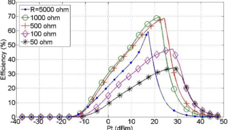
The diode vendor models are used in circuit simulation of effective efficiency by taking into account an input mismatch. The load is given as C = 82 pF and
R = 820 Ω. Fig. 1.23 presents the effective efficiency against the transmitted
power. HSMS-2820 produces high efficiency for high power levels. HSMS-2850 has good performance for low power levels. HSMS-2860 obtains high efficiency for medium power levels. In the aim of achieving the best efficiency, each diode should cooperate with its optimal load for given power levels.
Table1.1 presents the typical parameters for Schottky diode HSMS-28xx [50].
BV is the reverse breakdown voltage. IBV is the current at the breakdown voltage.
EG is the band gap energy. Every solid has its own characteristic energy band
structure. The band gap energy of semiconductors tends to decrease with
increas-ing temperature. XT I is the saturation-current temperature exponent (3 for P-N
junction; 2 for Schottky). XT I and EG take part in defining the dependence of Is.
Vf is the forward voltage drop, which is corresponding to the forward current
If. It is an important parameter that must be considered in diode simulations. The
Chapter 1. Introduction 27 Diode Type SMS1546 SMS76210 SMS7630 MA4E1317 BV(V) 3 3 2 7 Cj0(pF) 0.38 0.1 0.14 0.02 EG(eV) 0.69 0.69 0.69 0.69
IBV(A) 10E-5 10E-5 10E-4 10E-4
Is(A) 3E-7 4E-8 5E-6 10E-8
N 1.04 1.05 1.05 1.5 Rs(Ω) 4 12 20 4 Vj(V) 0.51 0.51 0.34 0.323 XT I 2 2 2 2 M 0.36 0.35 0.4 0.5 Vf 200-270mV (If=1mA) 260-320mV (If=1mA) 60-120mV(If=0.1mA) 135-240mV(If=1mA) 700mV (If=1mA)
Table 1.2: Typical parameters of other Schottky diodes
current (0.1 mA). Even in the condition of the forward current 1 mA, the forward voltage of HSMS-2850 is lower than HSMS-2810, HSMS-2820, and HSMS-2860. It means that HSMS-2850 can be turned on by the lowest power level. This diode may be the best choice for the application of very low power. But it is not advised for the frequency band that we desire.
In the bibliography study, other diodes [51,52] are also taken into account by
using the simulated model and the SPICE model. In comparison of SPICE
param-eters on the data sheets [53, 54], as presented in Table 1.2, HSMS-2820 is perfect
for RF-to-DC conversion of high power levels due to small series resistance and large breakdown voltage. MA4E1317 and HSMS-2860 are both suited to constitute rectifying circuits for low power levels. But compared with MA4E1317, HSMS-2860 has larger saturation current, smaller emission coefficient, larger junction potential, and thus better efficiency.
These diodes from HSMS-28xx family are surface mount RF Schottky barrier
diodes. They are all encapsulated in SOT-23 package. Thus it is interesting
to design rectifying circuits for high power levels with HSMS-2820 and for low power levels with HSMS-2860 due to diode characteristics. HSMS-2850 owns very low forward voltage and it operates well in low power levels. In the following sections, rectifying circuits are designed with these diodes according to specific requirements.
Chapter 2
State of The Art
2.1
Configuration of rectennas
A rectenna contains an antenna and a rectifying circuit. The antenna collects the microwave power. The rectifying circuit converts the RF energy into useful DC energy. The conversion is done by a non-linear element, usually Schottky diode. Thus rectifying circuits have non-linear characteristics.
A rectifying circuit is made up of a combination of Schottky diodes, input RF filter, output capacitor, and resistive load. Generally, the input RF filter is a band pass filter which rejects harmonics created by diodes. Matching circuits are needed between the antenna and the rectifying circuit with the aim of minimizing the mismatch loss and ameliorating the overall efficiency.
Several configurations have been used to convert the microwave power into
useful DC power, such as half bridge circuits [55] and whole bridge circuits [56].
According to the requirement of output DC voltage and conversion efficiency, single
serial diode circuits [57, 58], single shunt diode circuits [59, 60], voltage doubler
circuits [61], and multi-step voltage doubler circuits [62] have been considered, as
shown in Fig. 2.1. All the configurations of rectifying circuits should be accurately
optimized to maximize the conversion efficiency [63].
For a given incident power, the efficiency of rectifying circuits is altered by the conduction loss of diodes and the impedance mismatching, as well as the dielectric and metallic losses. The diode loss is inevitable. It is one of dominant factors for
(a) Single serial diode
(b) Single shunt diode
(c) Voltage doubler
(d) Two-step voltage doubler
Figure 2.1: Topologies of rectennas
the rectification of either low power levels or high power levels. In addition, the efficiency of rectifying circuits affects the overall efficiency of rectennas.
Structures with single series or shunt diode have an advantage of minimizing the conduction loss introduced by diodes. The structure of voltage doubler obtains higher output DC voltage than the case of single diode under the same condition of input power levels. The voltage doubler has more diodes in parallel participating in the rectification process. It brings higher output DC voltage but it is not efficient due to more conduction loss. It is interesting to make a compromise between RF-DC conversion efficiency and DC output voltage.
We desire a rectifying circuit which gives high DC voltage and high efficiency even if incident power levels are low. So the single diode configuration is a good