HAL Id: tel-01374739
https://tel.archives-ouvertes.fr/tel-01374739
Submitted on 1 Oct 2016HAL is a multi-disciplinary open access archive for the deposit and dissemination of sci-entific research documents, whether they are pub-lished or not. The documents may come from teaching and research institutions in France or abroad, or from public or private research centers.
L’archive ouverte pluridisciplinaire HAL, est destinée au dépôt et à la diffusion de documents scientifiques de niveau recherche, publiés ou non, émanant des établissements d’enseignement et de recherche français ou étrangers, des laboratoires publics ou privés.
Electronic and thermoelectric properties of
graphene/boron nitride in-plane heterostructures
van Truong Tran
To cite this version:
van Truong Tran. Electronic and thermoelectric properties of graphene/boron nitride in-plane het-erostructures. Materials Science [cond-mat.mtrl-sci]. Université Paris Saclay (COmUE), 2015. En-glish. �NNT : 2015SACLS133�. �tel-01374739�
NNT : 2015SACLS133
THESE DE DOCTORAT
DE L’UNIVERSITE PARIS-SACLAY,
préparée à l’Université Paris-Sud
ÉCOLE DOCTORALE N° 575
Electrical, Optical, Bio – physics and Engineering (EOBE)
IEF - Institut d'Electronique Fondamentale
Spécialité de doctorat : Electronique et Optoélectronique, Nano et Microtechnologies
Par
Van-Truong Tran
Propriétés électroniques et thermoélectriques des hétérostructures planaires de
graphène et de nitrure de bore
Thèse présentée et soutenue à Orsay, le 26 Novembre 2015 : Composition du Jury :
M. VOLZ Sebastian EM2C, CNRS Président M. GOUPIL Christophe LIED, Université Paris Diderot Rapporteur M. PALA Marco IMEP-LAHC, CNRS Rapporteur M. SAINT-MARTIN Jérôme IEF, Université Paris-Sud Examinateur M. DOLLFUS Philippe IEF, CNRS Directeur de thèse
i
Contents
Contents ... i List of figures ... v Acknowledgements ... xv Abstract ... 1 Résumé ... 2 Introduction ... 12 1 Chapter 1: ... 171.1 The semi-empirical methods ... 17
1.1.1 Tight Binding model for electron study ... 18
1.1.2 Force Constant model for phonon study ... 21
1.1.3 Matrix representation for Tight Binding and Force Constant calculations ... 23
1.1.4 Operator form of Tight Binding Hamiltonian ... 26
1.1.5 Eigen value problem for infinite periodic structures ... 28
1.2 Physical quantities that can be obtained from band structure ... 30
1.2.1 Bandgap ... 30
1.2.2 Density of states and local density of states ... 31
1.2.3 Electron and hole distributions ... 31
1.2.4 Group velocity ... 32
1.2.5 Effective mass ... 32
ii
1.4 Green's function method ... 34
1.4.1 General definition of a Green's function ... 34
1.4.2 Green's function in Physics. Atomistic Green's function ... 35
1.4.3 Green's functions for an open system ... 36
1.4.4 Calculation of DOS by Green function ... 37
1.5 Physical quantities obtained from transport study ... 38
1.5.1 Calculation of the Transmission from Green's function ... 38
1.5.2 Local density of states ... 39
1.5.3 Electron current ... 40
1.5.4 Conductance ... 41
1.5.5 Thermoelectric effects ... 42
1.6 Computational Techniques ... 44
1.7 Examples: electrons and phonons in linear chain, graphene and Boron Nitride (BN). ... 45
1.7.1 Linear chain ... 45 1.7.2 Graphene ... 57 1.7.3 Boron Nitride ... 64 1.8 Conclusions ... 67 2 Chapter 2: ... 68 2.1 Introduction ... 68
2.2 The modeling and methodologies ... 73
iii
2.3.1 Bandgap opening in armchair Graphene/BN ribbons ... 76
2.3.2 Bandgap opening in zigzag Graphene ribbons ... 87
2.4 Conclusions ... 93
3 Chapter 3: ... 94
3.1 Introduction ... 94
3.2 Modelling and methodology ... 95
3.3 Results and discussions ... 97
3.3.1 Modulation of bandgap under effect of by a transverse electric field: First approach .. 97
3.3.2 Modulation of bandgap under effect of by a transverse electric field: Self-consistent study 102 3.3.3 Tuning of current using transverse electric fields ... 108
3.4 Conclusions ... 112
4 Chapter 4: ... 113
4.1 Introduction ... 113
4.2 Methodology ... 117
4.3 Results and discussion ... 119
4.3.1 Hybrid states in a “one-interface” structure ... 119
4.3.2 Hybrid states in a “two-interface” structure ... 122
4.3.3 Dispersion of hybrid states: specific properties ... 126
4.3.4 From the effective model to hybrid states: the role of B (N) atoms ... 129
4.3.5 Enhancement of electron transport from hybrid states ... 132
iv
4.3.7 The parity of wave functions ... 134
4.4 Conclusions ... 140
5 Chapter 5: ... 141
5.1 Introduction ... 141
5.2 Studied device and methodology... 145
5.2.1 Device structure ... 145
5.2.2 Methodologies ... 146
5.3 Results and discussion ... 150
5.3.1 Electron and phonon dispersions in infinite structure Graphene or BN/G/BN ribbons 150 5.3.2 Phonon scattering: a key to enhance ZT ... 152
5.3.3 Effect of temperature ... 161
5.3.4 Effect of vacancies: a further improvement ... 162
5.4 Conclusions ... 168
Summary and possible future works ... 170
Appendices ... 173
Appendix A: Solving 1D Poisson’s equation numerically ... 173
Appendix B: Green’s function of an open system and Dyson’s equation ... 177
Appendix C: Transmission with single layer matrix size calculation ... 179
Appendix D: Intermediate functions and Phonon conductance ... 184
Bibliography ... 186
v
Publications ... 196
Conferences ... 196
List of figures
Figure 1-1: A system consists of N atoms and in each atom M orbitals (sketched by red regions) contribute to conduction. ... 19Figure 1-2: Force Constant model with springs connect between atoms. [65] ... 22
Figure 1-3: Schematic view of vibration directions of each atom in a plan xoy and the rotational angle from i-th atom to j-th atom. ... 26
Figure 1-4: Diagram of energy bands in a solid body for different phases. ... 30
Figure 1-5: Exchanged energy in an open system X when it is connected to another system A. ... 36
Figure 1-6: Electron current in the device under a bias. ... 40
Figure 1-7: Fermi function as a function of energy for different temperatures from very low (4 K) to room temperature (300 K) and high temperature (700 K). ... 41
Figure 1-8: Flowchart of computational steps for Green's function techniques. ... 44
Figure 1-9: An infinite linear chain with 1 atom per unit cell. Onsite energy is E0 and hopping parameter is Ec. ... 45
Figure 1-10: Band structure of a periodic chain line for E0 = 0, Ec = -1 eV. ... 46
Figure 1-11: Device of N atoms. Hopping Energy between the atoms of the device and the contacts Ec’ is different from that between atoms in the contacts and the device Ec. Contacts are semi-infinite. .... 46
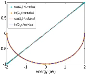
Figure 1-12: Comparison of numerical Sancho iterative technique and analytical results for Surface Green function. E0 = 0, Ec = -1 eV. ... 49
vi
Figure 1-14: Device of two atoms with energy connection between the atom of the device and contact is the same as energy between atoms in contacts ... 50
Figure 1-15: Comparison between Scattering method and Green's function method for a device with N = 2. ... 52
Figure 1-16: I-V characters in the device of a linear chain. Parameters are NA = 20; EfL = 0.1 eV, EfR
= 0.1 eV, E0 = 2.t0 , Ec = - t0 with t0 2 / 2 . .
m a e2
, m = 0.25m0 , a = 3×10⁻¹⁰ m. ... 53Figure 1-17: Vibration in a system of an infinite linear chain with two nearest atoms coupled by a spring with stiffness kc. ... 53
Figure 1-18: Phonon dispersion of a linear chain with one atom per cell ... 54
Figure 1-19: A device of chain lines for phonon study. kc and kd are the stiffness in the contacts and
device, respectively. k is the coupling between nearest atoms in the contacts and the device. ... 54
Figure 1-20: N = 10, kc = kd =2×10⁻¹⁰ N/m, a carbon atom has m = 1.994×10⁻²⁶ kg. ... 56
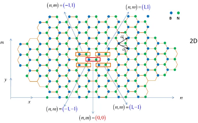
Figure 1-21: structure of 2D graphene. In nearest neighbor interaction, the unit cell (n,m) (red) only interacts with its four nearest cells. ... 57
Figure 1-22: 3D plot for electronic band structure of 2D graphene. The left panels: band structure and first Brillouin zone. The right panels: projections of the band structures on kx (upper) and ky (lower)
and the center figure is a Dirac cone around zero energy. ... 59
Figure 1-23: Comparison for the energy band and DOS (2D graphene) between our calculation and results obtained by Reich el all [55], Carpio el all [89]. All works were based on first nearest TB calculation with t = 2.7eV. Energy is plotted along high symmetrical directions MG-GK-KM. ... 60
Figure 1-24: Comparison of phonon dispersion between our calculation and results obtained by Wirtz el all [54]. FC model up to 4th nearest neighbor interaction, using off-diagonal parameters of Wirtz. . 60
Figure 1-25: Comparison of energy dispersion for armchair and zigzag Graphene ribbons. Energy is taken in unit of hopping parameter t. Reference: Nakada el al. [90] ... 61
Figure 1-26: Bandgap in armchair graphene is classified in 3 groups 3p, 3p + 1 and 3p + 2.
3 2p 3p 3 1p
vii
Figure 1-27: Transmission for different groups of Armchair graphene (a), (b), (c) and for zigzag graphene (d). ... 63
Figure 1-28: 2D structure of Boron Nitride (BN). The blue atoms are Boron and the green ones are Nitrogen atoms. ... 64
Figure 1-29: Electronic band structure of 2D BN. Here tBN = 1.95 eV; EB = 0; EN = -4.57 eV; [91] .... 65
Figure 1-30: Phonon dispersion of 2D BN. Force constant parameters are from ref.[92] ... 66
Figure 1-31: Comparison of phonon conductance for armchair BN ribbons. Reference: Ouyang, et al.[93] ... 66 Figure 2-1: (i) Illustration of the main steps of the synthesis process for in-plane Graphene/BN heterostructures. (ii) SEM images of graphene/h-BN stripes with (a) and (b) domains controlled by Photolithography with each strip width of about 10 µm, the scale bars are 50 mm and 10 mm, respectively. In (c) domains were controlled using FIB technique, the width of strips, from top to bottom, are 1 mm, 500 nm, 200 nm and 100 nm, respectively. Scale bar, 1 mm. Reference: Liu et al. [45] ... 69
Figure 2-2: Raman spectra collected in graphene, h-BN regions and their interface in a graphene/h-BN film. Reference: Liu et al. [45] ... 70
Figure 2-3: (a) STEM-ADF image shows the graphene/h-BN interface. The darker region is graphene and the other is BN. (b) EELS analysis with the inset is intensity profile along the trajectory in the dashed box, showing the sharp interface between the h-BN and graphene. (c) STEM bright field (BF) imaging of the graphene/h-BN interface. Reference: Liu et al. [45] ... 71
Figure 2-4: Armchair G/BN superlattice structure with graphene and BN sections arranged alternatively along transport direction Ox. There are NC Carbon lines and NBN Boron Nitride lines in
one unit cell. ... 74
Figure 2-5: Heterostructures of Armchair G/BN ribbons with interfaces parallel to the transport direction Ox. (a) Armchair G/BN structures with two sub-ribbons (b) Armchair G/BN/G ribbons with a BN ribbon embedded between two other Graphene ribbons. (c) Armchair BN/G/BN ribbons with a graphene ribbon embedded between two other BN ribbons... 75
viii
Figure 2-6: Energy bands of different armchair ribbons: (a) pure armchair graphene with M = 8, (b) superlattice G.BN with M = 8, NC = NBN = 2, (c) Armchair G/BN with MCC = 8, MBN = 8, (d) Armchair
G/BN/G with MCC1 = MCC2 =8, MBN = 8, (e) Armchair BN/G/BN with MBN1 = MBN2 =8, MCC = 8. ... 77
Figure 2-7: Bandgap for the case r = 1: (a) group M = 3n, (b) group M = 3n + 1, (c) group M = 3n + 2. ... 78
Figure 2-8: Bandgap in the superlattice armchair graphene/BN structures in the case where graphene dominates the supercell (r < 1). ... 79
Figure 2-9: Bandgap in the superlattice armchair Graphene/BN structure in the case where BN dominates the supercell (r > 1). ... 80
Figure 2-10: (a) Bandgap in armchair G/BN structure is plotted as function of (a) MCC and (b) MBN. (c) and (d) three groups of bandgap as a function of graphene ribbon width with MBN = 1 and 10, respectively. ... 82
Figure 2-11: Bandgap in the armchair G/BN/G structures as a function of MCC and MBN. ... 83
Figure 2-12: Bandgap in the armchair G/BN/G structures for the case MCC1 ≠ MCC2. ... 83
Figure 2-13: Bandgap in the armchair BN/G/BN structures as a function of MCC and MBN. ... 84
Figure 2-14: Comparison bandgap of pure armchair graphene ribbons and armchair Graphene/BN structures width different configurations. Here we fix MBN = 10 for all structures of graphene/BN. ... 85
Figure 2-15: Energy bands and density of states of (a) a superlattice structure with NC = 3, NBN = 1, M = 59 dimmer lines. (b) An armchair G/BN/G structure with MCC1 = MCC2 = 15, MBN = 29. ... 86
Figure 2-16: Comparison of group velocity in four armchair structures of the same width M = 59 dimmer lines. ... 87
Figure 2-17: Zigzag graphene/BN with two configurations: (a) B-C and (b) N-C connections at the interface. ... 88
Figure 2-18: (a), (b) Bandgap in the zigzag graphene/BN with B-C connections. (c), (d) bandgap in the zigzag graphene/BN with N-C connections. ... 89
ix
Figure 2-20: The zigzag BN/G/BN has three different configurations of interface connections: (a) B-C--C-B, (b) N-C--C-N, (c) B-C--C-N. ... 91
Figure 2-21: Bandgaps in (a) the zigzag G/BN/G and (b) the symmetrical zigzag BN/G/BN with B-C-C-B connections as a function of MCC for several values of MBN. ... 92
Figure 2-22: Full band structures in (a) zigzag G/BN/G and in BN/G/BN with (b) C--C-B and (c) B-C--C-N connections. ... 92
Figure 2-23: Tunable bandgap in the embedded zigzag BN/G/BN with B-C-C-N connections. ... 93
Figure 3-1: Schematic view of the Armchair G/BN/G structure studied in this work with MCC1 = MCC2
= 15, MBN = 29. It is placed in between two side gates that generate a transverse electric field. ... 96
Figure 3-2: P parallel regions with different permittivity in an external field generated by two side gates V- and V+. ... 97
Figure 3-3: The modulation of bandgap is a function of the electric field F0 for (a) Armchair G/BN/G
heterostructure for MCC1 = MCC2 = 15, MBN = 29, (b), (c), (d) Pure armchair Graphene for M= 15, 30,
59, respectively. ... 99
Figure 3-4: Revolution of energy bands in different structures: Figures (a1, a2, a3) with solid lines are band structures of Armchair G/BN/G for MCC1 = MCC2 = 15, MBN = 29. Figures b, c, d are band
structures of pure armchair Graphene for for MCC = M = 15, 30, 59 respectively. The strength of
electric field F0 is indicated in each panel. ... 100
Figure 3-5: (a), (b) Redistribution of charge in the system under effect of the electric field. (c), (d) Potential profile along the width of the ribbon with and without effect of charge redistribution (CR). Here, the external electric field is F0 = 3 and 9 mV/Å, respectively. ... 104
Figure 3-6: Typical potential profiles obtained for different external electric fields F0 = 3, 9, 15 and 20
mV/Å. ... 105
Figure 3-7: Plot of energy bands for four values of the external field F0 = 0, 3, 9 and 15 mV/Å. ... 106
Figure 3-8: Energy bangap of the hybrid ribbon and effective mass in the lowest conduction band as a function of the external field F0... 107
Figure 3-9: Schematic view of the Armchair Graphene/BN/Graphene structure studied in this work with MCC1 = MCC2 = 15, MBN = 29. It is placed in between two side gates that generate a transverse
x
electric field. For the transport analysis, a portion of this hybrid ribbon is connected to two graphene contacts. ... 108
Figure 3-10: Current as a function of bias voltage for transverse electric fields F0= 0, 5, 10 and
20 mV/Å. The simulation was performed at room temperature T = 300 K, and for EF = 0.2 eV in the
leads. The length of the active region is LA = 10.5 nm. ... 109
Figure 3-11: The current for the system of 17 nm in length and a bias Vb = 0.2 V is applied. The
current without (F0 = 0 mV/Å) and with electric field (F0 = 20 mV/Å) are IOFF = 7.54 × 10⁻⁶ I0, ION =
0.107I0, respectively with I0 = 2e/h . This result leads to an on/off current ratio ION/IOFF 14200. .. 111
Figure 3-12: The current at a low bias Vb = 0.1 V and no electric field is applied. This current
(OFF-current) becomes smaller when increasing the length of the active region. ... 111
Figure 4-1: A zigzag graphene ribbon (a) with its band structure near zero energy (b). Energy is degenerated at k = ±π and the flat bands are edge states. Reference: Wakabayashi et al.[73]... 114
Figure 4-2: Edge states in a quantum Hall bar Topological Insulator HgTe/CdTe: (a) energy bands of edge states in TI HgTe/CdTe with solid lines are for finite width system and the dashed lines are for 2D system. (b) and (c) density distribution of edge states at two opposite momentums kx and – kx, the
solid lines correspond to the upper edge state band and the dot lines correspond to the lower band. Reference: Zhou et al. [133] ... 115 Figure 4-3: (a) A graphene layer is sandwiched between two slabs Bi2Se3, (b) illustration of the system
under a pressure, (c) band structure without and with pressure. Reference: Kou et al. [141] ... 116
Figure 4-4. (a) Schematic view of zigzag Graphene/BN in-plane heterostructure with B-C bonds. The sub-ribbon widths are defined by the numbers of zigzag lines MCC = MBN = 50. (b) Decaying potential
Vdec related to B and N atoms in the layers L1 and L2 defined in (a), with BN/G boundary indicated by a vertical dashed line. Inset: magnification on the significant range of variation of Vdec. (c) Band
structure, with hybrid/edge states in solid red lines. Inset: schematic representation of the velocity direction of hybrid/edge states. (d) Profile of the probability density for the three states (1), (2) and (3) defined in (c). ... 120
Figure 4-5: (a) Sketch of one interface structure with N-C bonds. (b) Decaying potential Vdec in the layers L1 and L2. (c) Band structure, with hybrid/edge states in solid red lines. (d) Profile of the probability density for the three states (1), (2) and (3) defined in (c). Here MCC = MBN = 50. ... 122
xi
Figure 4-6: (a) Schematic view of a zigzag BN/G/BN structure with two C-B bond interfaces (B-C--C-B). (b) Energy band structure for MBN1 = MCC = MBN2 = 50. Inset: schematic representation of the
velocity direction of hybrid states at both interfaces (c) Profile of the probability density for the three states (1), (2) and (3) indicated in (b). ... 124
Figure 4-7: (a) Schematic view of a zigzag BN/G/BN with B-C--C-N bond interfaces. (b) Band structure for MBN1 = MCC = MBN2 = 50. (c) Profile of the probability density for the two states (1) and
(2) indicated in (b). (d) Bandgap as a function of sub-ribbon width MCC for different values of MBN. 125
Figure 4-8: (a) Comparison of lowest conduction and highest valence bands in the B-C--C-N structure for different graphene ribbon width MCC = 10 and 50. On each band, hybrid states are marked with
symbols and bulk states are in dashed line. (b) bulk/edge ratio (see text) in the highest valence band. The intersection of the slope in dashed line with the abscissa gives the value of kt separating edge
states and bulk states. ... 128
Figure 4-9: Group velocity of hybrid states as a function of the wave vector kx in different structures.
... 129
Figure 4-10: (a) Model of effective potential Veff applied on the edge atoms of a zigzag graphene
ribbons to mimic the effects of G/BN interface. (b-e) Energy bands for different effective potentials applied. (f) Square wave function corresponding to the state marked with a blue dot in (e). Inset: magnification of the interface region. ... 130
Figure 4-11: The new edge states in the effective potential model (symbols) compared with actual hybrid states (solid and dashed lines) in the B-C--C-N structure. ... 131
Figure 4-12: (a) Stepped B-C interface structure. (b) Energy bands for a pure zigzag graphene with MCC = 25 (solid black line), straight B-C interface with MBN = 25, MCC = 25 (dashed blue line) and MBN
= 30, MCC = 20 (dotted red line). Transmissions are plotted in the right panel for pure zigzag graphene
ribbon, straight B-C interface and the stepped B-C interface (dashed-dotted orange line). In the latter case we have MBN1 = 30, MCC1 = 20, MBN2 = 25, MCC2 = 25, N1 = N2 = 10. ... 132
Figure 4-13: Left panel: Graphene/BN heterostructures were grown on a (111) iridium single crystal with gold intercalated under the samples. Right panel: local density of states observed by Scanning Tunneling Spectroscopy (STS) at the interfaces. Reference: Drost et al. [145] ... 134
Figure 4-14: (a) The energy band of the B-C structure is plotted in the range of momentum from 0 ≤ kxax ≤ 2π. (b) Wave functions at states (1), (2), (3), (3’) in (a), filled and unfilled circles present the
xii
Figure 4-15: Energy bands and wave functions of a B-C-C-B structure with even MCC = 50 (and MBN2
= MBN2 = 50). Red circle with plus sign ‘+’ and blue circle with minus sign ‘-’ correspond to even/odd
states, respectively. ... 136
Figure 4-16: Energy bands and wave functions of a B-C-C-B structure with odd MCC = 51. Here, MBN2
= MBN2 = 50... 137
Figure 4-17: (a) An infinite zigzag graphene ribbon with an applied stepped potential. (b) and (c) band structures in each region and conductance for the case of odd and even MCC, respectively. In both
cases U = 0.5Δ. ... 138
Figure 4-18: (a) A stepped potential based on B-C-C-B structures. (b) and (c) band structures in each region and conductance for the case odd and even MCC. In both cases MBN1 = MBN2 = 25, U = 1.0Δ. 139
Figure 5-1: (a) The supper cell structures were considered by Yang et al.[163] and (b) the best result of ZT is about 0.7 at high chemical energy 1.58 eV... 143
Figure 5-2: A device made of hybrid zigzag ribbons of graphene/BN and two leads made of square lattices. The best ZT at room temperature (kT = 0.025 eV) is about 0.23. Reference: Vishkayi et al.[76] ... 144
Figure 5-3: Schematic view of studied graphene/BN heterostructure with sub-sections made of BN flakes attached to the main AGNR channel. The two leads are made of BN/G/BN ribbons as the hybrid parts of the active device. ... 146
Figure 5-4: Energy bands for two cases: MCC = 5 (metallic graphene) and MCC = 6 (semiconducting
graphene). Band structures for armchair BN/G/BN also plotted. DOSs are shown in the third column to illustrate the concentration of states in the two regions. ... 151
Figure 5-5: Phonon bands for (a) graphene ribbon and (b) BN/G/BN structure with MCC = 5. (c) DOS
for phonons are plotted for comparison. ... 152
Figure 5-6: Phonon conductance as a function of temperature for MCC = 5 (a), and MCC = 6 (b), for
different values of the number nBN of BN/G/BN sections. Phonon conductance at the room temperature
for (c) MCC = 5 (cyan circles) and (d) MCC = 6 (brown circles) as a function of nBN. ... 153
Figure 5-7: (a) & (b) Comparison of phonon transmissions in perfect graphene ribbons (dash lines) and the studied device (cyan and brown lines). For both panels Nvc = NBN = 8, nBN = 1. ... 154
xiii
Figure 5-8: (a) (b) Electrical conductance and (c) (d) Seebeck coefficient for the structures with (a) (c) MCC = 5 and (b) (d) MCC = 6 for different numbers nBN of BN/G/BN sections. Other parameters: T =
300K. ... 155
Figure 5-9: Phonon conductance is plotted as a function of the width of BN flakes. Here Nvc = NBN = 8
and nBN = 1. ... 156
Figure 5-10: Figure of merit was plotted for different length Nvc and NBN of graphene and BN/G/BN
sections. Fig (a) and (b) were examined with nBN = 1. The results agree that the best ZT for MCC = 5
and MCC = 6 are obtained if Nvc = NBN = 8. ... 158
Figure 5-11: (a) (b) Maximum of thermoelectric figure of merit as a function of nBN for (a) MCC = 5
and (b) MCC = 6. Thermoelectric figure of merit ZT as a function of chemical potential µ for (c) MCC =
5 and (d) MCC = 6. T = 300K. ... 159
Figure 5-12: ZT as a function of chemical potential for the thinnest ribbon MCC = 3 in the cases of pure
GNR (dashed line) and hybrid heterostructure with MBN = 11 (solid line), Nvc = 6, NBN = 4, nBN = 10, T
= 300 K. ... 160
Figure 5-13: Dependence of ZTmax on the GNR width MCC, depending on whether MCC can be written
in the form 3p, 3p + 1 or 3p + 2, with p is an integer number. MBN = 10, 11 for even, odd MCC,
respectively and Nvc = NBN = 5, nBN = 10. ... 161
Figure 5-14: ZT as a function of chemical potential for different temperatures T ranging from 100 K to 400 K for the heterostructure with MCC = 5. Here MCC = 5, MBN = 9, and nBN = 10. ... 162
Figure 5-15: (a) The broadening of gn functions with the increase of temperature. (b) The longest slop
of Seebeck coefficient shifts to the left when temperature becomes hotter. ... 163
Figure 5-16: Effect of a single vacancy on the thermoelectric properties for the structure with MCC = 5.
(a) The seven vacancy configurations investigated here. (b) Phonon conductance for the different vacancy configurations. ... 164
Figure 5-17: Effect of a single vacancy on the thermoelectric properties for the structure with MCC = 5.
ZT and power factor for the different configurations of vacancy in (a), (c) graphene and (b), (d) BN. Symbols correspond to results without any vacancy. T = 300 K. ... 165
xiv
Figure 5-18: Local current in different armchair graphene ribbons. From one edge to the middle of the ribbons, in all cases we can observe that charge distribution is lowest at lattice positions 3m. Reference: Wilhelm et al. [175] ... 167 Figure 5-19: Electron density in an infinite structure of armchair BN/G/BN for sub-ribbons width for Graphene and BN are MCC = 5 and MBN = 9, respectively. In the graphene part, the middle point has
the lowest charge. ... 167
Figure 5-20: Effect of two and three vacancies in the middle of the graphene ribbon on the figure of merit. MCC = 5, T = 300 K. ... 168
xv
Acknowledgements
I would like to send my heartfelt thanks and gratitude to my two supervisors Philippe Dollfus and Jérôme Saint-Martin for their kindness and the whole-hearted guidance during my PhD. I greatly appreciate their concern not only on my work but also on my life. I believe that without these helps my projects would never completed.
On this occasion, I would like to thank all my colleagues in COMICS group (Prof. Arnaud Bournel, Dr. Damien Querlioz, Dr. Michele Amato, Mr. Salim Berrada, Mr. Adrien Vincent,
Mr. Jérôme Larroque, Dr. Viet-Hung Nguyen, Ms. Thu-Trang Nghiem-Thi, Ms. Mai Chung
Nguyen and others) for a friendly atmosphere and also their help in life and works. Especially, Mr. Christophe Chassat for his helps in setting up my desktop and debugging computer problems.
It is also an opportunity for me to acknowledge Université Sud 11, Université Paris-Saclay and CNRS (Centre National de la Recherche Scientifique) for the financial supports. Finally, I would like to express my thanks and gratefulness to my parents, my brothers, my sister, my wife and my little daughter for their love, share and encouragement.
This work is dedicated for all people I love. Orsay, 01 September, 2015
1
Abstract
Graphene is a fascinating 2-dimensional material exhibiting outstanding electronic, thermal and mechanical properties. It is expected to have a huge potential for a wide range of applications, in particular in electronics. However, this material also suffers from a strong drawback for most electronic devices due to the gapless character of its band structure, which makes it difficult to switch off the current. For thermoelectric applications, the high thermal conductance of this material is also a strong limitation. Hence, many challenges have to be taken up to make it useful for actual applications.
This thesis work focuses on the theoretical investigation of a new strategy to modulate and control the properties of graphene that consists in assembling in-plane heterostructures of graphene and Boron Nitride (BN). It allows us to tune on a wide range the bandgap, the thermal conductance and the Seebeck coefficient of the resulting hybrid nanomaterial. The work is performed using atomistic simulations based on Tight Binding (TB), Force Constant (FC) models for electrons and phonons, respectively, coupled with the Green's function formalism for transport calculation.
The results show that thanks to the tunable bandgap, it is possible to design graphene/BN
based transistors exhibiting high on/off current ratio in the range 104-105. We also predict the
existence hybrid quantum states at the zigzag interface between graphene and BN with appealing electron transport. Finally this work shows that by designing properly a graphene ribbon decorated with BN nanoflakes, the phonon conductance is strongly reduced while the bandgap opening leads to significant enhancement of Seebeck coefficient. It results in a thermoelectric figure of merit ZT larger than one at room temperature.
2
Résumé
Le graphène, matériau bidimensionnel constitué d’une monocouche d'atomes de carbone formant un réseau en nid d'abeille, est bien connu pour ses exceptionnelles propriétés électroniques.[1] Sa structure de bandes d'énergie ne présente pas de bande interdite, avec une dispersion quasi-linéaire autour du point de neutralité. Enfin la mobilité électronique y est extrêmement élevée.[2] Parmi ses nombreux autres avantages, ce matériau présente également des propriétés thermiques et mécaniques exceptionnelles, dont une très forte conductivité thermique [3] et une aptitude à supporter de grandes déformations.[4] On espère donc qu'il puisse donner lieu à un grand nombre d’applications.[5] La structure de bande et les propriétés du graphène ont d'abord été étudiées théoriquement par Wallace dès 1947.[6] Cependant, la limitation des techniques expérimentales à cette époque n'a pas permis aux scientifiques de confirmer les fascinantes propriétés prédites théoriquement. Il a fallu attendre 2004 pour que Geim et son étudiant Novoselov réussissent à isoler une forme stable de graphène en exfoliant une seule couche de carbone à partir de graphite.[7] Cet avancée scientifique a démontré l'existence d'un matériau bidimensionnel à base de carbone, qui a alors été nommé graphène. Ensuite, le graphène est rapidement devenu pour les physiciens un sujet de recherche très en vogue, aussi bien d’un point de vue fondamental qu’au niveau des applications.
En dépit de ses excellentes propriétés électroniques, le graphène présente des inconvénients qui en limitent certaines applications, notamment en électronique. Tout d'abord, il est impossible de bloquer complètement le courant dans des dispositifs en graphène du fait de l'absence de bande interdite dans la structure électronique. Un autre problème est la croissance du graphène et son dépôt sur des substrats isolants. Comme le graphène est très mince, la
surface assez rugueuse du SiO2, souvent utilisé comme substrat, peut piéger les charges et
modifier la forme plane du graphène,[8,9] ce qui affecte fortement le transport électronique. En effet, bien que la mobilité des électrons dans le graphène doit théoriquement pouvoir
atteindre environ 200 000 cm2⋅V−1⋅s−1 à température ambiante,[5] une telle valeur n’a été
obtenue que dans du graphène suspendu (sans substrat). [2] Pour le graphène sur SiO2, la
meilleure mobilité expérimentale mesurée est d'environ 40 000 cm2⋅V−1⋅s−1,[10] mais elle est
généralement beaucoup plus basse, ce qui est loin des attentes initiales. Ainsi, le choix du substrat est d'une grande importance en vue de parvenir à des applications électroniques hautes performances.
3
Le graphène est également prévu pour être appliqué dans le contexte de la spintronique. Même si le couplage spin-orbite dans le graphène est très faible et incapable de séparer les électrons à spin "up" et les électrons à spin "down",[11] dans des rubans de graphène avec des bords zigzag, il est possible de fabriquer des filtres de spin grâce à la séparation de spin dans des états de bord de faible énergie.[12,13] Toutefois, seuls des rubans de graphène extrêmement étroits de type zigzag sont pertinents pour exploiter cet effet.
En ce qui concerne les propriétés thermoélectriques, le graphène souffre de limitations intrinsèques malgré son excellente mobilité électronique. L'absence de bande d'énergie interdite fait qu'il est difficile de séparer les contributions opposées d'électrons et de trous pour l'effet Seebeck qui y est donc faible.[14] En outre, comme mentionné ci-dessus, la propagation des phonons est également très bonne dans le graphène ce qui est une autre limitation pour les applications thermoélectriques.[3] En effet, la capacité thermoélectrique
d'un matériau est évaluée par la figure de mérite thermoélectrique ZTG S Te 2 /
KeKp
qui est définie par l'intermédiaire de la conductance électriqueGe, le coefficient Seebeck S et
la conductance thermique des électrons et des phonons (Ke et Kp). Ainsi, avec un très faible
coefficient Seebeck et une très haute conductance thermique, le ZT du graphène est faible, inférieur à 0.01, alors qu'un matériau thermoélectrique efficace doit avoir ZT ~ 1. Pour rendre le graphène plus propice à la thermoélectricité, certaines stratégies de conception et nanostructuration doivent être appliquées pour à la fois améliorer le coefficient Seebeck et aussi réduire la conductance thermique.
En fait, en raison de l'énorme potentiel du graphène, les scientifiques ont cherché continuellement des solutions pour en surmonter ses limites. Fondamentalement, la recherche sur le graphène a connu différentes périodes. Avant 2004, seulement quelques travaux théoriques prédisaient des propriétés intéressantes du graphène. Après la découverte expérimentale de graphène, de 2004 à 2010 la plupart des travaux ont été axés sur le graphène pur, visant essentiellement à ouvrir une bande interdite dans sa structure de bandes en exploitant les structures 1D de graphène (rubans de graphène) [15-18] ou en appliquant des champs électriques perpendiculaires aux bicouches de graphène.[19] D'autres propriétés physiques ont été également étudiées comme l'effet Hall quantique et les interactions de spin.[20-22] Au cours des dernières années, les activités de recherche sur le graphène ont été élargies vers de nombreuses orientations visant à trouver de nouvelles propriétés pour de
4
nouvelles applications. Ces recherches peuvent être classérs en quatre grandes tendances de recherche :
(i) L'étude de nouveaux effets sur le graphène tels que (1) le dopage avec des atomes substitutionnels tels que le bore ou de l'azote pour ouvrir une bande iterdite [23]; (2) la découpe d'un réseau périodique de trous dans les feuilles de graphène [24]; (3) la fonctionnalisation avec l'hydrogène, nommée graphone [25,26]; (4) la construction d’une logique ultra-faible puissance à mémoire non volatile à l'aide de la grande longueur de diffusion du spin dans le graphène 2D [27,28]; (5) l’étude des effet géométrique comme la rugosité de bord, les défauts ou les torsions [29]; (6) l’amélioration de la performance thermoélectrique en utilisant des géométries sophistiquées.[30-33]
(ii) L'étude d'hétérostructures entre le graphène et d'autres matériaux: (1) l'ouverture de bande interdite avec des structures hybrides de graphène/BN,[34-37] (2) l’utilisation de substrat de haute qualité en nitrure de bore hexagonal qui est en accord de maille quasi parfait avec le graphène et qui est lisse.[38]
(iii) L'étude de nouvelles propriétés des matériaux 2D comme le graphène tels que MoS2, SiC,
phosphorène et silicène. De plus ils ont l’avantage de présenter une bande interdite intrinsèque et un fort couplage spin-orbite.[39]
(iv) L'étude de nouveaux allotropes de carbone: ce sont des matériaux à base de carbone mais qui ont une structure légèrement différente du graphène comme le pentagraphène (structures pentagonales) [40] ou le Graphyne et le graphdiyne avec des structures circulaires.[41,42]
En ce qui concerne la tendance de la recherche sur les hétérostructures graphène/BN, récemment des expérimentateurs ont démontré avec succès la synthèse de structures de graphène/BN sur une seule couche, [43-45] ce qui a motivé certaines études théoriques sur les structures de bandes électroniques [34,35,46,47 ] et aussi sur le transport [46,48-51] dans ce nouveau matériau hybride.
Dans ce contexte, ce projet de thèse a été consacré aux propriétés des hétérostructures planaires de graphène/BN dans le but de comprendre et d'améliorer leurs propriétés électroniques et thermoélectriques par rapport au graphène 2D. Il se concentre particulièrement sur l’ouverture d’une bande interdite et sur les propriétés de transport qui peuvent être utilisées pour réaliser de bons transistors ou de bons convertisseurs d'énergie.
5
L'étude est basée sur des méthodes semi-empiriques comme celles des liaisons fortes pour les électrons et celles des constantes de force pour les phonons. Ces méthodes ont été largement utilisées en physique de la matière condensée en raison de leur efficacité de calcul. Nous utilisons aussi les fonctions de Green hors équilibre (NEGF) combinées avec les approches atomistiques mentionnées plus haut pour étudier le transport quantique.
Une visite guidée de la thèse
Ce manuscrit de thèse est organisé en cinq chapitres et quatre annexes.
Chapitre 1 : Contexte théorique
Dans ce chapitre, je présente le contexte théorique de mon étude. Tout d'abord, les méthodes empiriques, y compris les modèles « liaisons fortes » et « constantes de forces », sont examinées. L'équation de Schrödinger pour les électrons et l'équation de mouvement de Newton pour les phonons peuvent être formulées dans un problème aux valeurs propres, à savoir, respectivement . . H CE C (1) et 2 U DU (2)
Dans l'équation (1), H est le Hamiltonien électronique, E est l'énergie et C les fonctions
d'ondes locales. Dans l'équation (2), fait référence à la fréquence de vibration des phonons,
U est le vecteur de déplacement dans l'espace et D est la matrice décrivant la dynamique de couplages entre les atomes.
Dans le cas où le système est périodique, ces problèmes de valeur propre peuvent être réduits à l'équation pour une cellule élémentaire
. 0 0 .ei k R R H H E
(3)où H est le Hamiltonien des électrons (ou la matrice dynamique des phonons) pour une
6
Connaissant les bandes d'énergie (ou la dispersion des phonons) et la fonction d'onde, certaines grandeurs physiques telles que la bande interdite, la densité d'états (DOS), la densité locale d'états (LDO), la densité de charge, la vitesse de groupe, la masse effective peuvent être calculées.
Pour étudier le transport dans les systèmes hors-équilibre, les fonctions de Green d’un système ouvert qui est connecté à des contacts (gauche et droite) sont introduites. Elles sont calculées par
1D D L R
G EH (4)
où HD est le Hamiltonien de la région active ("Device") et L R DL R gL R L R D est la self-energy du contact gauche (droite). Ensuite, la transmission peut être calculée par l'intermédiaire de la fonction de Green par la formule de Meir-Wingreen
†
L D R D
T trace G G (5)
où L R i L R L R † (6)
sont appelés les taux d'injection au niveau des contacts.
Avec la transmission obtenue par expression (5), d'autres quantités de transport, par exemple, le courant, la conductance, le coefficient Seebeck, le facteur de mérite ZT peuvent être calculés.
Les principales étapes de calcul et les différentes techniques utilisées pour calculer les propriétés de transport sont indiquées dans le chapitre.
Dans la dernière partie de ce chapitre, la modélisation et les méthodes ci-dessus sont appliquées pour examiner les propriétés électroniques et thermiques de certains systèmes simples comme la chaîne linéaire d'atomes ainsi que des structures 2D et 1D de graphène et de Nitrure de Bore hexagonal.
Chapitre 2 : Hétérostructures graphène/BN avec une bande interdite accordable et des électrons à haute vitesse
7
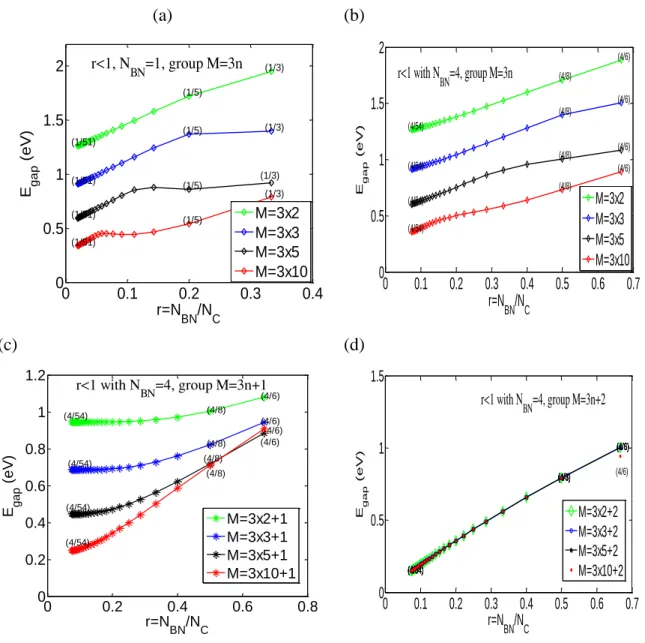
Dans ce chapitre, je présente les mécanismes d'ouverture de la bande interdite et sa modulation dans des hétérostructures de graphène/BN. Les bandes interdites de différentes configurations de rubans « armchair » et « zigzag » sont étudiées en utilisant un calcul de liaisons fortes fondé sur un modèle simple d'interaction au premier voisin. L’étude permet de comprendre quelles configurations présentent une bande interdite intéressante. Elle démontre que les structures hybrides avec des interfaces parallèles à la direction du transport conservent de bonnes propriétés de transport (vitesse de groupe élevée), meilleures que dans les structures avec des interfaces perpendiculaires à la direction de transport comme on le voit dans la Figure 1. Il est également montré que toutes les hétérostructures « armchair » sont semi-conductrice avec une bande interdite. Les structures « zigzag » sont soit métalliques soit semi-conductrices, selon le type de couplage à l'interface entre le graphène et le BN.
Figure 1: Comparaison de la vitesse de groupe dans quatre structures « armchair » de même
largeur M = 59.
Chapitre 3 : Modulation de largeur de bande interdite et du courant dans des nanorubans de graphène/BN sous champ électrique transverse
0.2 0.4 0.6 0.8 1 0 0.2 0.4 0.6 0.8 1 k x(1/nm) Gr o u p ve lo ci ty (1 0 6 m
/s) Pure armchair Graphene Armchair G/BN/G
Armchair supper lattice G.BN Pure armchair BN
8
Dans ce chapitre, j’étudie l'effet d'un champ électrique dans le plan sur les bandes d'énergie d'une structure « armchair » G/BN à deux rubans de graphène séparés par un ruban BN comme esquissé dans la Figure 2 (a). Tout d'abord, une première approche simple est appliquée pour étudier l'effet d'un champ électrique externe dans différentes structures, y compris le G/BN armchair et des rubans armchair de pur graphène avec l'hypothèse que le potentiel électrostatique est linéaire (donc sans auto cohérence avec l’équation de Poisson). Cette approche simple nous montre que la structure G/BN/G présente un net avantage par rapport à de simples rubans de graphène : l’application d’un champ électrique externe permet de moduler efficacement la largeur de la bande interdite.
Ensuite, j’étudie cet effet dans la structure G/BN armchair en prenant en compte l'effet de redistribution de charge en résolvant les équations de Schrödinger-Poisson couplées:
0
0 0 0 V H U E (7)L'évolution de la bande interdite avec l'étude d'auto-cohérente montre que la bande interdite est fortement réduite sous l'effet d'un champ électrique de moins de 20 mV/Å. En outre, l'effet de redistribution de charge reste faible pour un champ électrique inférieur à 6 mV/Å. Avec la modulation de la forte largeur de bande interdite sous l'effet du champ électrique, le courant est commandé avec succès dans un dispositif hybride constitué d'un ruban de graphène/BN comme montré sur la Figure 2 (b). Le rapport des courants ON et OFF à la polarisation
Vbias = 0.2 V est défini comme le rapport des courants à F0 = 20 mV/Å et au F0 = 0 mV/Å. Il
est de 3830 pour une longueur de la région active de 10.5 nm et atteint même jusqu'à 14200 si cette longueur est de 17 nm.
9 (a) (b) 0 0.1 0.2 0.3 0.4 10-6 10-5 10-4 10-3 10-2 10-1 100 V bias (V) C u rr e n t( 2 e /h ) F 0 = 20 mV/Å F 0 = 0 F 0 = 5 mV/Å F 0 = 10 mV/Å
Figure 2: (a) Vue schématique de la structure graphène/BN/graphène armchair étudiée. Le
système est placé entre deux grilles latérales qui génèrent un champ électrique transversal. La région active est connectée à deux contacts de graphène. (b) Courant en fonction de la tension
de polarisation pour des champs électriques transversaux F0 = 0, 5, 10 et 20 mV/Å. La
simulation a été effectuée à température ambiante T = 300 K, avec EF = 0.2 eV. La longueur
de la région active est LA = 10,5 nm.
Chapitre 4 : Etats hybrides dispersifs et transport quantique dans des hétérostructures graphène/BN
Dans ce chapitre, j’étudie l'émergence d'Etats qui sont localisés à l'interface des hétérostructures zigzag de graphène/BN. Pour des résultats précis, les interactions juqu’au deuxième voisin sont prises en compte
, ,
dec
i i j i j i
i i j i j i
H
i i
t i j
t i j
V i i (8)Un potentiel Videc est également ajouté pour reproduire les calculs ab initio.
L'étude est reprise pour différentes configurations d'hétérostructure G/BN zigzag. L'analyse de la structure de bandes indique que les états de bords au niveau des interfaces de G/BN (Figure 3 (a)) sont robustes par rapport aux états de bords dans des rubans zigzag de pure graphène. Ces états ont (courbes rouges dans la Figure 3 (b)) des vitesses de groupe très
10
élevées jusqu'à 7.4×10⁵ m/s. La transmission due à l'émergence de ces états, subit une
amélioration significative, qui se répercute sur la conductance électrique à basse énergie. Les états d'interface robustes survive aussi dans des structures en G/BN zigzag avec des interfaces imparfaites. En outre, on étudie l'effet de la parité pour comprendre les propriétés de transport dans des structures graphène/BN zigzag.
(a) (b)
Figure 3: (a) vue schématique d'un zigzag BN/G/BN avec interfaces B-C--C-N (b) la
structure de bande pour MBN1 = MCC = MBN2 = 50 et le profil de la densité de probabilité pour
les deux états (1) et (2). Une largeur de bande peut être clairement observée dans la figure (b).
Chapitre 5 : Amélioration de la performance thermoélectrique dans des hétérostructures graphène/BN
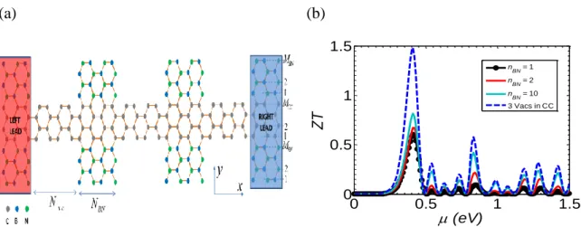
Dans le chapitre 5, j'étudie les propriétés thermoélectriques d'hétérostructures de graphène/BN constituées d'un ruban de graphène décorés par des nano-flocons de BN régulièrement espacés (Figure 4 (a)). Cette géométrie efficace engendre une forte réduction de la conductance des phonons par rapport à celle des rubans de graphène. De plus, une bonne conductivité électrique est conservée car la présence du BN, qui est un isolant, sur les côtés du graphène n’affecte pas la cionduction électrique. Il en résulte une valeur élevée de ZT de 0,81
pour un ruban hybride avec MCC = 5 (Figure 4 (b)). Le pic de ZT peut être observé à basse
énergie µ = 0,41 eV, ce qui est beaucoup plus faible que dans le cas de structures en super-réseau transverse. Les effets de la température et des lacunes sur les propriétés thermoélectriques sont également étudiées. Remarquablement, les lacunes au centre du ruban
-1 -0.5 0 0.5 1 -1.5 -1 -0.5 0 0.5 1 1.5 k xax/ E ( e V ) B-C N-C (1) (2) B-C N-C 0 30 60 90 120 150 0 0.05 0.1 0.15 0.2 0.25 0.3 0.35
atom position along y
2 ( a rb . u n it) BN1 graphene BN2 (2) (1)
11
de graphène peuvent conduire à une amélioration supplémentaire du facteur de mérite ZT. Avec trois lacunes introduites dans le canal, un ZT de 1,48 est obtenu (Figure 4 (b)).
(a) (b) 0 0.5 1 1.5 0 0.5 1 1.5 (eV) ZT nBN = 1 n BN = 2 n BN = 10 3 Vacs in CC
Figure 4: (a) Vue schématique de l’hétérostructure de graphène/BN avec des flocons BN. (b)
La figure de mérite thermoélectrique ZT en fonction du potentiel chimique μ pour le MCC = 5
et T = 300K.
Enfin, une partie de l'étude est consacrée aux conclusions et perspectives. Les principales contributions de ce travail de thèse sont mises en évidence et les futurs travaux possibles sont discutés. Enfin, quatre annexes présentent la méthode numérique de résolution de l'équation de Poisson, les bases du formalisme NEGF pour un système ouvert arbitraire, et le calcul de la formule de transmission. La bibliographie et la liste des publications de l'auteur sont données à la fin du manuscrit.
12
Introduction
Graphene, a monolayer (two-dimensional) material made of carbon atoms arranged in a honeycomb lattice, is now well-known for its exceptional electronic properties,[1] with gapless and quasi-linear dispersion around the neutrality point and extremely high intrinsic electron mobility.[2] Among many other features, this material also offer outstanding thermal and mechanical properties with very high thermal conductivity[3] and ability to sustain large strain.[4] It is thus expected to give rise to a large number of various applications.[5] The band structure and related properties of Graphene were first studied theoretically by P. R. Wallace since 1947.[6] However, the limitation of experimental techniques at that time did not allow scientists to confirm these fascinating predicted properties. In 2004, Geim and his student Novoselov isolated successfully a stable form of Graphene by exfoliating a single layer of carbon from graphite.[7] This event demonstrated the existence of a two dimensional carbon-based material, which was later named Graphene. Then, Graphene rapidly become a hot research topic in physics from fundamental up to application viewpoints.
Besides its excellent electronic properties, Graphene has some drawbacks which makes it not directly suitable for applications. First, it is impossible to switch off completely the current in devices made of Graphene as Graphene is lacking of a bandgap. Another problem is the growth of Graphene and its deposit on insulating substrates. As an insulator stable at high
temperature and easy to process, silicon dioxide (SiO2) has been frequently used as a substrate
for Graphene in experiments and devices. However, as Graphene is very thin, the rough SiO2
surface causes charge trapping on the surfaces and modifies the planar shape of Graphene,[8,9] which strongly affect the electronic transport in Graphene. Indeed, although the electron mobility in Graphene has theoretically predicted to reach around
200 000 cm2⋅V−1⋅s−1 at room temperature,[5] such a high value has been obtained only for
suspended (substrate-free) Graphene.[2] For Graphene on SiO2, the very best experimental
mobility achieved is about 40 000 cm2⋅V−1⋅s−1,[10] but it is usually much below, which is far
from the initial expectations. Thus, the choice of substrate is of high importance with a view to reach high performance electronic applications.
Graphene is also expected to be applied in the context of spintronics. Even if the spin orbit coupling in Graphene is very weak and unable to separate spin up and down,[11] in Graphene
13
ribbons with zigzag edges, it is possible to make spin filters thanks to the separation of spin at low energy edge states.[12,13] However, only extremely narrow zigzag Graphene ribbons are relevant, i.e. ribbons wherein edge states at two sides are close enough to be able to interact. Regarding thermoelectric properties, Graphene suffers from intrinsic limitations though it has an excellent electron mobility. This is due in particular to the lack of energy gap in 2D Graphene that makes it difficult to separate the opposite contributions of electrons and holes to the Seebeck effect and leads to a very small Seebeck coefficient.[14] Additionally, as mentioned above, the phonon propagation is also confirmed to be very good in Graphene, which is another limitation for thermoelectrics.[3] Indeed, the thermoelectric ability of a material is assessed by the thermoelectric figure of merit ZT which is defined via the electrical
conductance Ge, the Seebeck coefficient S and the thermal conductance of electron and
phonon (Keand Kp) as
2
/
e e p
ZT G S T K K . Hence, with extremely small Seebeck
coefficient and very high thermal conductance, 2D Graphene has very small ZT which in fact is less than 0.01, while an efficient thermoelectric material needs ZT~1. To make Graphene more suitable for thermoelectrics, some strategies of nanostructuring design need to be applied to enhance the Seebeck coefficient and reduce the thermal conductance.
Actually, due to the huge potential of Graphene, scientists have been continually seeking solutions to overcome its limitations. Basically, research on Graphene underwent different periods. Before 2004, just few theoretical works predicted interesting properties of Graphene. After the experimental discovery of Graphene, from 2004 to 2010 most of works were focused on pure Graphene, essentially aiming at opening a band gap by exploiting 1D structures of Graphene (Graphene ribbons),[15–18] on applying perpendicular electric fields in bilayer Graphene.[19] Other physical properties were also investigated such as the quantum Hall effect and the spin interactions.[20–22] In recent years, research activities on Graphene were broadened towards many new directions aiming at finding novel properties for new applications. These researches can be classified into four main research trends:
(i) The study of new effects on Graphene such as (1) doping with atoms such as Boron or Nitrogen into Graphene sheet to open a mini gap[23]; (2) cutting Graphene into Graphene nanomesh with periodic holes in the sheets[24]; (3) Graphene with Hydrogen functionality named as Graphene and graphone[25,26]; (4) using the large spin diffusion length in 2D Graphene to build up ultra-low power non-volatile logic and memory through spin current
14
processing[27,28]; (5) effect of geometrical shape such as edge roughness, defects, strain or twisted Graphene[29]; (6) enhancement of thermoelectric performance by reducing phonon conductance using sophisticated designs.[30–33]
(ii) The study of heterostructures of Graphene and other materials: (1) opening wider band gap of Graphene with hybrid structures of Graphene/BN[34–37], (2) high quality substrate for Graphene using hexagonal Boron Nitride thank to the perfect match in crystal structures of these two materials and the flatness of h-BN surface [38].
(iii) The study of new properties of Graphene-like materials: some 2D materials have similar
structures than Graphene such as MoS2, SiC, Phosphorene and Silicene but they exhibit
intrinsic bandgap and strong spin-orbit coupling.[39]
(iv) The study of new allotropes of carbon structures: these are carbon-based materials which have a slightly different structure like Graphene-like penta-Graphene (pentagonal structures)[40] or Graphyne and graphdiyne with circle structures.[41,42]
Regarding the research trend on Graphene/BN heterostructures, recently experimentalists have successfully demonstrated the synthesis of Graphene/BN structures in a single sheet [43–45], which has motivated some theoretical studies on electronic band structures [34,35,46,47] and also on transport[46,48–51] in this new hybrid material.
In such context, this PhD project has been devoted to the properties of in-plane heterostructures of Graphene/BN with the aim at understanding and improving their electronic and thermoelectric properties with respect to pristine Graphene. It particularly focuses on bandgap opening and transport properties that can be applied in transistors or energy converters. The study is based on semi-empirical methods like Tight Binding (TB) model for electrons and Force Constant (FC) model for phonons. These methods have been widely used in condensed mater physics because of their efficiency in calculation and reasonable computation time. We also use the atomistic non-equilibrium Green's function (NEGF) approach for studying quantum transport as it can be easily combined with the semi-empirical methods mentioned above.
15
A guiding tour to the thesis:
This thesis manuscript is organized in five chapters and four appendices.
In Chapter 1, I present the theoretical background of my study. First, the empirical methods including Tight Binding and Force Constant models are reviewed. Then, some physical quantities which can be obtained from band structures are introduced. The following section presents atomistic Green’s function method and some transport properties that can be computed using this formalism. Next, the electronic and thermal properties of some textbook cases such as the linear chain of atoms, 2D and 1D structures of pristine Graphene and hexagonal Boron Nitride are presented.
In Chapter 2, I present the bandgap opening and its modulation in in-plane Graphene/BN heterostructures. The energy band diagram and bandgap for different configurations of armchair and zigzag Graphene/BN ribbons are investigated using simple Tight Binding calculation based on a first nearest neighbor interaction model. The investigation will help us to understand which configurations of Graphene/BN with a finite bandgap could be interesting for applications.
In chapter 3, I study the effect of an in-plane electric field to energy band of an armchair G/BN structure with two Graphene ribbons separated by a BN ribbon. First, a first simple approach is applied to investigate the effect of an external electric field in different structures including the armchair G/BN and pure armchair Graphene ribbons with the assumption that electrostatic potential in each homogeneous region is linear. Next, I study this effect in the armchair G/BN structure including the effect of charge redistribution by solving self-consistently of the coupled Schrödinger-Poisson equations. The evolution of bandgap with the applied electric field is then applied to control the current in a device made of a hybrid Graphene/BN ribbon.
In chapter 4, I investigate the emergence of states which are localized at the interface of zigzag Graphene/BN heterostructures. These states have peculiar properties which contribute to enhance significantly the electron transport in zigzag Graphene structures. Besides, the parity effect is also investigated to understand transport properties of zigzag Graphene/BN structures.
16
In chapter 5, I show our proposal of a Graphene/BN heterostructures that exhibit appealing thermoelectric performance. By using an efficient design, in this structure the phonon conductance is strongly reduced with respect to pure Graphene ribbons and a good electrical conductance is kept. The effects of temperature and vacancies on thermoelectric properties are also investigated.
Finally, a section is dedicated to the conclusions and perspectives. The main contributions of this thesis work are emphasized and the related possible future works are discussed. Four appendices (presenting derivations of some important formulas), the bibliography and the list of author’s publications can be found at the end of the manuscript.
17
1
Chapter 1:
Theoretical Background
In this chapter we intend to review the main theoretical concepts and numerical methods that directly relate to this PhD work. The chapter covers the review of (i) semi-empirical methods including Tight Binding and Force Constant models, (ii) the physical quantities that can be deduced from band structure, (iii) the Green’s function formalism of quantum transport for investigating nanostructures. These models and methods are finally applied to investigate some basic electronic and thermal properties of several systems such as linear chain, graphene and Boron Nitride as illustrative examples.
1.1 The semi-empirical methods
Before reviewing the main features of Tight Binding (TB) and Force Constant (FC) models widely used in this work, we would like to discuss the reasons why we chose these semi-empirical methods for our study.
It is well known that ab initio methods are powerful tools to investigate material properties in condensed matter physics because they directly derive from first principles of quantum mechanics, with the highest possible level of accuracy. They usually give very good agreements with experimental results.[52] In spite of their advantage in providing reliable results, the use of these techniques is rapidly limited when dealing with devices of reasonable size as computational costs could easily exceeds the capacity of current computers. In fact, current ab initio methods can only be applied for small systems with limited number of atoms (about a few tens of atoms), while computation of larger systems still faces with many challenges. It is thus required to consider other efficient methods to be able to deal with larger systems of a few hundreds or thousands of atoms.
Tight Binding and Force Constant models are semi-empirical methods that do not require a fully self-consistent process for the computation of electron and phonon dispersions, and thus are much faster compared to ab initio calculations. However, they require the prior knowledge of some given empirical parameters which are called onsite and hopping energies in electron study and force constant parameters in phonon study. These parameters are usually adjusted so that dispersion results from Tight Binding (or Force Constant) simulation fit well with that
18
of ab initio calculation or experiments.[52–54] With good selected parameters it has been demonstrated that the semi-empirical methods may give good agreements with ab initio and experimental results, especially at low energy [55] or low frequency ranges [54]. Thus Tight Binding and Force Constant models are considered to be useful tools for investigation of large systems, especially in devices, with reasonable computational efforts and time. They are now widely used.
Recently, the combination of ab initio and semi-empirical calculations has led to powerful approaches to study structures and devices at a multi scale level. Within such multi scale methodology, ab initio techniques are first applied to investigate small systems and then to generate parameters for the semi-empirical models such as Tight Binding. The obtained parameters are then used for semi-empirical simulations to study energy bands for larger systems, and can be combined with other quantum methods such as Green's functions or scattering matrix for the study of transport.[56]
1.1.1 Tight Binding model for electron study
The Tight Binding method is widely used by many physicists because it can not only reproduce well results from more complex and accurate methods such as ab initio, but also quickly allows scientists to predict quantitative results on the basis of a simple and physically meaningful model. Great success were evidenced from many works on many materials and devices, including graphene.[6,37,57–61]
The Tight Binding (TB) method is based on the theory of atomic orbitals. The term “tight binding” means that in solids electrons are tightly bound to the atom that they belong to and thus the electrons have limited interactions with surrounding atoms in the solid. Thus the overlap of wave functions between two adjacent atoms is very limited, which makes orbitals in solids close to that in atomic orbitals of free atoms.
Though Tight Binding technique was applied very soon for the study of graphene in 1947 by Wallace,[6] the complete parametrized Tight Binding method was actually generalized by John Clarke Slater in 1954.[62] It is also sometimes known as Linear Combination of Atomistic Orbital (LCAO) method, in particular in chemistry.
Mathematically, Tight Binding calculations can start with a basis consisting of the atomic orbitals of all atoms. In general, a system can contain N atoms and each atom has M orbitals