HAL Id: hal-03106821
https://hal.archives-ouvertes.fr/hal-03106821
Submitted on 12 Jan 2021
HAL is a multi-disciplinary open access
archive for the deposit and dissemination of
sci-entific research documents, whether they are
pub-lished or not. The documents may come from
teaching and research institutions in France or
abroad, or from public or private research centers.
L’archive ouverte pluridisciplinaire HAL, est
destinée au dépôt et à la diffusion de documents
scientifiques de niveau recherche, publiés ou non,
émanant des établissements d’enseignement et de
recherche français ou étrangers, des laboratoires
publics ou privés.
Distributed under a Creative Commons Attribution - NonCommercial| 4.0 International
License
Arbiterless Event-Based Imager Architecture with
temporal and spatial redundancies suppression
Mohamed Akrarai, N. Margotat, G. Sicard, Laurent Fesquet
To cite this version:
Mohamed Akrarai, N. Margotat, G. Sicard, Laurent Fesquet. Arbiterless Event-Based Imager
Archi-tecture with temporal and spatial redundancies suppression. 6th International Conference on
Event-Based Control, Communication, and Signal Processing (EBCCSP 2020), Sep 2020, Krakow, Poland.
�hal-03106821�
Arbiterless Event-Based Imager Architecture with
temporal and spatial redundancies suppression
Mohamed Akrarai
1, Nils Margotat
1,
2Gilles Sicard,
1Laurent Fesquet
1 Univ. Grenoble Alpes, TIMA, F-38031 Grenoble CNRS, TIMA, F-38031 Grenoble 2 CEA LETI Grenoble.
Abstract—We present a new image sensor architecture that manages spatial and temporal redundancies with an arbiterless readout and a pixel Address-Event Representation (AER) reading system. This frameless image sensor only generates few events over time in order to target an efficient power consumption compared to the commercial CMOS image sensors. Indeed, this image sensor does not generate anymore frames but events only when a change appears in the scene. Moreover, the event throughput depends on the luminance variations of the recorded scene. This means that more activity in the scene will generate more events and vice versa. Collecting events over a period of time will define an image. It is noticeable that, at each instant, the generated events characterize the zone of interest (the active area) of the scene. Consequently, processing such images should require less computing, communication and energy.
Index Terms—Event-based, Image sensors, Dynamic vision sensor, AER communication.
I. INTRODUCTION
Power efficient systems are of a great importance to insure a responsible exploitation of resources. Thus, adopting the concept of event driven systems is a solution for a better management of both hardware and energy resources. The event driven approach is beneficial for many applications, especially embedded systems with limited resources such as connected objects. In this perspective, image sensors are systems, critical in power consumption, which can be improved by adopting the event driven concept.
Asynchronous image sensors efficiently utilized this ap-proach, thanks to the Address Event Representation (AER) communication protocol, non uniform sampling techniques and clock-less readout which is the basic concept of asyn-chronous circuits and the driving motive behind their usage and advantages [1], [2]. Indeed, the main issue faced by image sensors is the usage of a clock signal coupled to the Shannon sampling scheme, which produce a huge amount of useless samples, extra-computation and communications. Standard image sensors provide at their output a constant frame rate and often high resolution words resulting from the power consuming analog-to-digital conversion. Contrarily, event based image sensors do not have such constraints as reading the whole pixel matrix, thanks to the usage of event based pixels.
The first developed event based pixel is the Time to First Spike (TFS) pixel [3]. It encodes the luminance information
by the integration time required by the photodiode voltage to cross a threshold. This pixel indicates the threshold crossing by an event and communicates the coordinates of the fired matrix pixels through an AER based communication. AER communication requires the pixel matrix to be surrounded by arbiters, to insure that only one event is communicating to the bus at a time. However, when the pixel matrix has a huge number of pixels, the arbitration takes time, which could result in timing errors. A unique pixel in the state-of-art is the DVS pixel [4], [5]. This pixel is unique in terms of suppressing temporal redundancies intrinsically at the pixel level. The pixel generates a set of ON and OFF polar events according to the slope of photocurrent change in its photodiode. This pixel also uses arbiters to communicate AER events. As a result, it suffers from event collision and bus saturation while reacting to a highly active scene. Similarly, many other asynchronous image sensors in the art suffer from similar problems [6], [7] and require timing assumptions to cope up with the saturation. An image sensor readout system that does not use arbiters was proposed in [8]. It has been integrated in an event-based image sensor enabling fast acquisition of events and spatial redundancies suppression. however, this system still suffers from some problems that will be discussed in detail later on in this paper (section II-D). Recently, spatial redundancies suppression of polar events (ON & OFF) generated by the DVS image sensor was introduced [9], and since its pixels already manage temporal redundancies at the pixel level, this image sensor completely suppresses all redundancies of polar events. However, as its predecessor in [4] it relies on row and column arbiters to communicate.
In this paper we will present a novel image sensor architec-ture, that does not rely anymore on arbiters to communicate data and suppresses completely redundancies. First, we present the operating principle of each pixel we use in our image sensor. Then, through simulation of the Matlab model of the readout system [8], we will list its drawbacks and how our architecture can improve its limitations. Finally, we choose one image sensor architecture out of few others we will suggest. The choice will be underpinned with statistical results and the event throughput relevance in terms of image quality and sensitivity to noise.
II. THETFSAND THEDVSPIXELS
Both TFS & DVS pixels use AER protocol to communicate their events, however the internal structure of the two pixels
greatly differs, as well as their operating principles, since they fulfill different functionalities.
A. The DVS pixel
It is mostly an analog pixel including a transducer amplifier, that converts photocurrent Iphinto a voltage Vpproportional to
log(Iph). The following stage of the pixel samples the Vpand
differentiates every two successive samples. The result is then compared to two thresholds. One threshold to generate ON events and the other to generate OFF events (figure 1a). Com-municating the events to the outside of the pixel matrix goes through the address event interface that includes an address encoder, handshake logic circuit and an arbiter (figure 1b).
(a) DVS pixel operating principle
(b) Block level schematic of a pixel array embedded in AER communication periphery
Fig. 1: DVS pixel operating principle and abstracted readout architecture.
B. The TFS pixel
This pixel operates as a one level-crossing sampling circuit. When the photodiode voltage Vphcrosses an externally defined
threshold, an AER event is generated. The event is in the form of a couple of coordinates (X,Y) representing the coordinates of the pixel in the pixel matrix. In order to translate this event into a gray level information, an external Time to Digital Converter is used. The TDC generates the instant at which it received the event coded in a bit vector depending on the image resolution. The high level image sensor architecture
of the TFS image sensor is represented in 2a. The readout system acquires the generated addresses and time-stamps to get the integration times. The event addresses and their time stamps are inserted into two parallel FIFOs, one for addresses and the other for time stamps. Inside the readout system is also a verification block. The verification block is a finite state machine that handles and distinguishes false from correct events. To understand how the verification block operates, Figure 2b illustrates an example of how the verification block operates with 16-pixel matrix. In the figure, both TFS pixels (X1, Y1) and (X3, Y3) trigger events, as a result, the output
row address is 1010 and the output column address is 1010, these two addresses also communicate the information that pixels (X1, Y3) and (X3, Y1) (colored in yellow) triggered,
which is false. This requires polling all the four pixels to know which have events and which don’t. Hence, as the same process has to be done for the whole pixel matrix, the readout system contains a verification block.
(a) TFS image sensor high level view in [8]
(b) Illustration of the verification problem
Fig. 2: TFS image sensor reading system architecture de-scribed in [8].
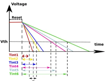
C. The TFS pixel and spatial redundancies suppression
Fig. 3: Spatial redundancies suppression principle. The readout system mainly suppresses spatial redundancies by clustering integration times that are relativity close to each other. For every received event, with integration time T inti
that verifies:
T inti≤ T intref+ ∆t (1)
T inti will be assigned T intref, with T intref being the
integration time of the first event. This way different pixels (Xi,Yi) in the resulting image will be given the same gray
level value that correspond to the TDC encoding of T intref.
For example in figure 3, events e1,e2and e3with integration
times T int1,T int2 and T int3, can all be suppressed into
T int1, since T int2≤ T int1+ ∆t and T int3≤ T int1+ ∆t.
Consequently, increasing ∆t will result in a higher compres-sion.
D. The TFS pixel readout system verification overhead In order to have an idea of the processing time overhead required to run the necessary verifications when reading the pixel matrix, we have developed a Matlab model of the readout system and the TFS image sensor. This model input is a stimuli from a 10-second video: a video of a car on the road, which is a normal case scenario for image sensors. From the model simulation output, we measured the event rate and verifications required to pinpoint the correct events. Figure 4, shows how severe is the amount of verifications required for uncertain events, and most importantly how verifications scale with the pixel matrix. We have found out that in the case of no spatial redundancy suppression, verifications represent 98% of the total data exchange between the pixel matrix and the readout system for a pixel matrix resolution of 600 × 1200 pixels, and 97.7% for 480 × 840 (wide VGA) pixels, and 97.3% for 360 × 630 pixels. This also means that 97% of the processing time will be spent trying to locate correct events in the pixel matrix. Consequently, suggesting an event based image sensor
architecture with AER communication without arbiters, should absolutely account for this verification overhead.
Fig. 4: The number of events and verifications required to process a 10-second stimuli for different pixel matrix dimensions.
III. THE NOVEL EVENT BASED IMAGE SENSOR ARCHITECTURE
After having explained how the TFS and the DVS pixels operate, we can have a closer look into how the combination of these two pixels, is beneficial to achieve a complete redun-dancy suppression, and how it can decrease the verification overhead at the readout system level. In the sequel, we present an improved arbiterless event-based image sensor architecture. A. The hybrid pixel matrix
To obtain a complete redundancy suppression, while also maintaining only the relevant gray level information, which is always required for standard image processing algorithms (that heavily rely on the standard frame rate CMOS image sensors), we suggest a novel image sensor architecture, consisting in a hybrid pixel matrix based on the combination of the DVS and the TFS pixels. (a) (b) (c) (d) (e) (f) .. . ... ... ... ... ... ... ... ... ... ... ... ...
(g) Architecture (a) pixel matrix .. . ... ... ... ... ... ... ... ... ... ... ... ... (h) Architecture (b) pixel matrix
Fig. 5: The different kernels of the pixel matrix and some examples of their full pixel matrix.
Our idea, combining these two pixels, is to use the DVS pixel to trigger the TFS pixels once a luminance change is detected. This way, the TFS pixel only captures the rele-vant luminance information and encodes it into a gray level
information using its TDC. Thus, the architecture manages temporal redundancies at the pixel level and spatial redundan-cies at the system level using the readout system presented in [8]. In figure 5, we present different sets of DVS and TFS combinations. (a) represents one DVS pixel (in Green) triggering one TFS pixel (in Blue), (b) features one DVS pixel triggering three surrounding TFS pixels and similarly in this order, in (c),(d) and (e) kernels the DVS pixel is surrounded by 5, 8 and 24 TFS pixels. Kernel (f) is particular, where the DVS pixel circuit uses the photodiodes of the surrounding 4 TFS pixels and takes the average photo-current of the four as input. Constructing a pixel matrix from one of these 5 kernels would be the result of repeating the kernels several times, like the pixel matrix (g) and (h) obtained from (a) and (b) kernel. In order to evaluate the kernels performances in terms of generated events, we have developed Matlab models of the two pixels and then run behavioral simulation of each kernel.
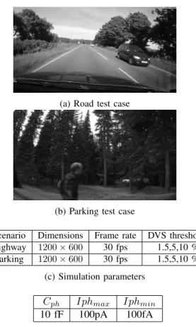
B. Test cases of the simulation
To evaluate the behavior of each pixel kernel matrix to different types of stimuli, we used two test cases. The first one is a road car driver view (High activity scene 6a). The second one is a parked car view with almost no activity, just a person walking in front of the car for a few seconds (Low activity scene 6b).
The simulation inputs are videos. The modeled kernel is applied to every video frame, hence generating the output of a pixel matrix formed by the kernel in question. For each scenario, the video lasts 10 seconds at a frame rate of 30 fps with 1200 × 600 pixels per frame. Thus, having a stimulus of 2.16×10⁸events, which is also the output of a standard CMOS image sensor, since it reads all the frames with no redundancy suppression. Each kernel undergoes 6 simulations represented in figure 6c, 2 scenarios × 3 DVS threshold cases. The analog characteristics of the photodiode used by both the DVS and TFS pixels are presented in the table 6d.
Both TFS and DVS pixels receive input as a current, as the video frames are converted to logarithmic photo-current. For this simulation, we set up the TFS voltage threshold at 2.3 Volts and the DVS threshold (defined in equation (2) bellow) to be the minimum photo-current change capable of triggering an event (when the DVS threshold increases, less events are generated and vice versa):
T hreshold(%) = ∆ log(Iph) log(Iphmax
Iphmin)
(2)
Finally, in order to present the effect of applying spatial redundancy suppression, we implemented a basic logic model of the readout system.
(a) Road test case
(b) Parking test case
Scenario Dimensions Frame rate DVS thresholds Highway 1200 × 600 30 fps 1.5,5,10 %
Parking 1200 × 600 30 fps 1.5,5,10 % (c) Simulation parameters
Cph Iphmax Iphmin
10 fF 100pA 100fA
(d) Photodiode parameters
Fig. 6: Illustration of the two test cases, the simulation parameters and the photodiode analog characteristics used in the model of the TFS pixel.
IV. SIMULATION RESULTS
In this section we present and compare the results of each architecture in terms of generated events and run verifications, as well as image quality and some kernels immunity to noise.
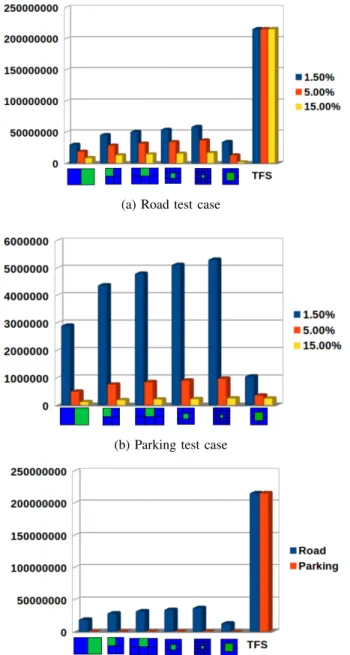
A. Events throughput
Figures 7a and 7b confirm at a first look that the event output of all architectures is indeed proportional to the scenes activity. As expected, reducing DVS threshold results in more DVS pixels detecting luminance change and triggering more TFS pixels. Therefore, more events will be detected. Also, from the two figures, we notice that the more TFS pixels surrounding a DVS pixel, the more events that will be generated. Finally, all of the hybrid architectures generated far less events than a standard CMOS and TFS image sensors would do for the same input, at least 70 % less events in the Road test case and 96 % less events in the parking test case, as figure 7c shows.
(a) Road test case
(b) Parking test case
(c) Comparison between our architectures (DVS threshold 1.5 %) and a standard CMOS in the two test cases
Fig. 7: The total number of generated events through the whole duration of stimuli: (a) and (b) represent the total number of events generated in each test case per DVS threshold, (c) comparison of the different architectures with standard image sensor (at 1.5% DVS threshold).
B. Verification processing
As the readout system has to process events through verifi-cations to pinpoint the correct events, we also tested the effect of applying Spatial Redundancy Suppression (SRS) (∆t > 0) on the number of required verifications. Figure 8 bellow, shows that indeed applying SRS decreases effectively the number of required verifications. Increasing ∆t results in requiring less verifications to spot the correct events.
Fig. 8:Comparison of the required verification operations by a TFS image sensor and the kernel (f)-based image sensor.
C. The image memory and image quality
The data generated by the pixel matrix are sent to update the image memory. At the initial instant of the simulation, all photodiodes generate a spike of photocurrent due to the sudden change in the scene luminance from darkness at t0−δt
to viewing the input scene at t0+ δt, as a result almost all
DVS pixels trigger the TFS pixels, which also integrate a full image of the scene. Consequently, the image memory is filled. Afterwards, the image memory is constantly updated with new data from the triggered TFS pixels in the pixel matrix. Hence, the resulting output of the image sensor is a frameless image constantly updating its pixels. Figure 9, illustrates the resulting image in the image memory and the flow of new events updating it.
(a) The original scene (b) The resulting image
(c) The freshly detected events
Fig. 9: (a) The viewed scene (b) The resulting image generated by pixel matrix of kernel f at 1.5% DVS threshold and no SRS (∆t = 0). (c) The flow of the new data events updating the image memory.
Figure 10, shows the effect of processing the generated TFS events through our readout system model. This system has applied spatial redundancy suppression on pixel outputs that have already suppressed their temporal redundancy internally. The two figures display the effect of proportionally increasing ∆t to the maximal detectable integration time. The result of increasing ∆t is a higher compression and a lower throughput at the price of a low image quality and vice versa.
(a) ∆t =T intmax
16 (b) ∆t =
T intmax
2
Fig. 10: The effect of applying spatial redundancy suppression, kernel (f).
Regarding the quality of the output images, only kernel (f) has a comparable output to the original image scene, since it has a full resolution of TFS pixels. The other kernels generate images with empty pixels at the coordinates of the DVS pixels in the pixel matrix. Obtaining a good quality will require even further processing to reconstruct in the image memory. The kernel (f) presents a Structural SIMilarity index (SSIM) of 0.93 (the ideal SSIM is 1) and a Peak Signal to Noise Ratio (PSNR) of 33.8 dB. This moderate image quality is mainly due to the DVS threshold setting: the lower the DVS threshold, the more updated the image memory. We choose the lowest DVS threshold to be 1.5% since it corresponds to the lowest attainable threshold in the state of the art [10].
D. Immunity to noise and the DVS thershold
At low DVS thresholds noise is dominant, meaning that incorrect events are often generated. In figure 7b, kernel (f) displays a lower event throughput than the other architectures at low DVS threshold (1.5 %) especially in scenes with low activity (figure 7b). This is mainly due to the averaging of the photocurrents of the surrounding four TFS pixel photodiodes and to the fact that noise is usually spatio-temporally uncorre-lated. Rarely, noise will affect less than two TFS photocurrents in four adjacent photodiodes and generate a stronger average photocurrent triggering the whole Kernel.
V. CONCLUSION
Our proposed image sensor architectures make the event rate proportional to the scene activity and give a completely compressed bitstream keeping most of the original scene efficiently, especially for kernel (f). Indeed, the output of these image sensor architectures is highly compressed and processable, which is useful for low power vision applications, since processing such a compressed output in realtime will require far less computing resources.
We are currently implementing an image sensor pixel matrix architecture based on kernel (f) in 28 nm FDSOI technology. We believe that this cutting edge technology will enable even better performances like a lower DVS threshold.
VI. ACKNOWLEDGMENT
This work has been partially supported by the OCEAN12 project
(H2020-EU.2.1.1.7 no78327)
REFERENCES
[1] Spars, Jens & Furber, Steve. (2001). Principles of Asynchronous Circuit Design: A Systems Perspective. 10.1007/978-1-4757-3385-3.
[2] Beerel, Peter & Ozdag, Recep & Ferretti, Marcos. (2010). A Designer’s Guide to Asynchronous VLSI.
[3] Chen Shoushun and A. Bermak, ”A low power CMOS imager based on time-to-first-spike encoding and fair AER,” 2005 IEEE International Symposium on Circuits and Systems, Kobe, 2005, pp. 5306-5309 Vol. 5.
[4] P. Lichtsteiner, C. Posch and T. Delbruck, ”A 128×128 120 dB 15µs Latency Asynchronous Temporal Contrast Vision Sensor,” in IEEE Journal of Solid-State Circuits, vol. 43, no. 2, pp. 566-576, Feb. 2008. [5] Lichtsteiner, Patrick & Delbruck, Tobi & Kramer, J.. (2005). Improved
ON/OFF temporally differentiating address-event imager. Proceedings of the 11th IEEE International Conference on Electronics, Circuits and Systems, 2004. ICECS 2004. 211 - 214. 10.1109/ICECS.2004.1399652. [6] C. Posch, D. Matolin and R. Wohlgenannt, ”An asynchronous time-based image sensor,” 2008 IEEE International Symposium on Circuits and Systems, Seattle, WA, 2008, pp. 2130-2133.
[7] E. Culurciello and R. Etienne-Cummings, ”Second generation of high dynamic range, arbitrated digital imager,” 2004 IEEE International Symposium on Circuits and Systems (IEEE Cat. No.04CH37512), Vancouver, BC, 2004, pp. IV-828.
[8] A. Darwish, L. M. G. Rocha, L. Fesquet and G. Sicard, ”Design of a fully asynchronous image sensor reading system,” 2015 Conference on Design of Circuits and Integrated Systems (DCIS), Estoril, 2015, pp. 1-5.
[9] C. Li, L. Longinotti, F. Corradi and T. Delbruck, ”A 132 by 104 10µm-Pixel 250µW 1kefps Dynamic Vision Sensor with Pixel-Parallel Noise and Spatial Redundancy Suppression,” 2019 Symposium on VLSI Circuits, Kyoto, Japan, 2019, pp. C216-C217.
[10] Serrano-Gotarredona, Teresa and Bernab Linares-Barranco. A 128 × 128 1.5% Contrast Sensitivity 0.9% FPN 3µs Latency 4 mW Asynchronous Frame-Free Dynamic Vision Sensor Using Transimpedance Preampli-fiers. IEEE Journal of Solid-State Circuits 48 (2013): 827-838.
![Fig. 2: TFS image sensor reading system architecture de- de-scribed in [8].](https://thumb-eu.123doks.com/thumbv2/123doknet/13485738.413724/3.918.509.800.424.1018/fig-tfs-image-sensor-reading-architecture-scribed.webp)