HAL Id: hal-01348477
https://hal.archives-ouvertes.fr/hal-01348477
Submitted on 24 Jul 2016
HAL is a multi-disciplinary open access
archive for the deposit and dissemination of
sci-entific research documents, whether they are
pub-lished or not. The documents may come from
teaching and research institutions in France or
abroad, or from public or private research centers.
L’archive ouverte pluridisciplinaire HAL, est
destinée au dépôt et à la diffusion de documents
scientifiques de niveau recherche, publiés ou non,
émanant des établissements d’enseignement et de
recherche français ou étrangers, des laboratoires
publics ou privés.
Effect of CMOS Technology Scaling on Fully-Integrated
Power Supply Efficiency
Gaël Pillonnet, Nicolas Jeanniot
To cite this version:
Gaël Pillonnet, Nicolas Jeanniot. Effect of CMOS Technology Scaling on Fully-Integrated Power
Supply Efficiency. 9th International Conference on Integrated Power Electronics Systems (CIPS 2016),
Mar 2016, Nuremberg, Germany. �hal-01348477�
Effect of CMOS Technology Scaling
on Fully-Integrated Power Supply Efficiency
Gaël Pillonnet
1, Nicolas Jeanniot
1,21 Univ. Grenoble Alpes, F-38000 Grenoble, France
CEA, LETI, MINATEC Campus, F-38054 Grenoble, France
2 Univ. of Lyon, CPE department, F-69616, Villeurbanne, France
Abstract— Integrating a power supply in the same die as the
powered circuits is an appropriate solution for granular, fine and fast power management. To allow same-die co-integration, fully integrated DC-DC converters designed in the latest CMOS technologies have been greatly studied by academics and industrialists in the last decade. However, there is little study concerning the effects of the CMOS scaling on these particular circuits. To show the trends, this paper compares the achievable efficiencies of the 2:1 switched capacitor DC-DC converter topology under the same constraints in 65, 130 and 350nm bulk CMOS nodes and 28nm in bulk and FDSOI technologies with various capacitor options.
Keywords— Fully-integrated power supply, switched capacitor converter, on-chip voltage regulator, power management scaling.
I. INTRODUCTION
Power management in embedded systems faces several technical challenges. First, the size of the power supplies which distribute the power from the battery to all circuits cover up to one third of the motherboard surface mainly due to their numerous passive components. Secondly, the recent processing circuits such as multi-core processors need various and fast-modulated power rails to optimize their power consumption [1]. Thirdly, the designer has to deal with the dense power rail routing and numerous dedicated power pins in the high power density circuit packages. Lastly, the power supply validation at system-level is done during the final design stage. To overcome these challenges, burying the power supply close to or in the powered circuits is a key solution, and to do this, the power electronics and VLSI communities have to work together to find relevant solutions for dense and efficient in-package or on-chip power supplies.
The power supply in package i.e. point of load (PoL) concept is now widely-used in some embedded systems. In addition, some companies provide small and highly-efficient step-down regulators with integrated power MOSFETs, inductors and capacitors in a single package. To propose a better integration, some work has studied the performance of on-chip power supplies in the last decade. There are two major approaches: i) 3D IC packaging [2,3] and ii) on-die voltage regulators. The first uses dedicated layers to provide high-density passive components stacked with the powered circuits through high density 3D connections. The second approach i.e. the on-die solution, relies on powered circuit technology being suitable for efficient power supply design. Due to the CMOS process limitation [4], inductorless DC-DC converter topology i.e. switched capacitor converter (SCC) has been well studied
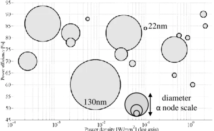
in the literature [5-7]. Fig. 1 shows the classical Figure of Merit (FoM) (power density v. efficiency) of an on-die SCC published in the last decade [8-24]. However, there is no clear link between the achievable power density and the technology node. Moreover, the technology impact is difficult to distinguish from the design refinements and environment constraints (ratio, input voltage, and power level, etc.). It is therefore clear that comparison of the SCC under the same conditions over a large CMOS technology nodes range has been insufficiently studied [25].
Fig. 1. Power density v. efficiency for different technology nodes
This paper provides a contribution to on-chip power supplies by studying the effect of major CMOS technology nodes on the power supply performance especially the power efficiency of SCCs. First, the SCC losses are described and a model is given to have a physical insight into the efficiency optimization. Based on this analysis, extraction of the key technology parameters is explained. Then, these parameters are given for major CMOS technology nodes. Based on transistor-level simulations and an optimization procedure, the maximal SCC efficiencies are given over a large silicon surface range for three different CMOS technologies (130, 65, 28nm) and capacitor options (MOS, MIM, deeptrench) for a 2:1 converter using a 1.8V input voltage.
II. SCCEFFICIENCY ANALYSIS
A. 2:1 Switched Capacitor Converter Topology
The SCC topology is studied here because of its inductorless property and integration capacity proved in the CMOS process [26]. N to M conversion ratios in SCC topology are possible [27], but 2:1 SCC achieves the best power efficiency. Therefore in this paper, the most efficient SCC
diameter α node scale 130nm
topology is chosen in order to study the maximal achievable efficiency [28], [29]. Other ratios will have lower performance.
Fig. 2. 2:1 switched capacitor converter (SCC) schematic
The 2:1 SCC reduces the input voltage rail Vin to the output voltage Vout by a factor of two under ideal and open-circuit conditions. This topology mainly consists of a flying capacitor Cfly charged and discharged in two phases by four switches as shown in Fig. 2. In the first phase, ϕ1, T1 and T4 are in on-state and the capacitor is charged from the input voltage through the output load. In the second phase, ϕ2, the flying capacitor is discharged into the load through transistors T2 and T3. Between the two phases, a dead time is introduced to avoid cross-conductions between the output, input and ground terminals.
B. Efficiency Modelling
The SCC has inherent losses (charge-sharing loss) due to the charge and discharge of the flying capacitor Cfly through the on-state resistance of the switches T1,2,3,4. [30] has already derived the electrical equations for 1:1 SCC. From this work, the conduction loss Pcond for a 2:1 SCC can be expressed as:
𝑃𝑐𝑜𝑛𝑑= 𝛽 coth (𝛽2) 𝑅𝑜𝑛𝑖𝑜𝑢𝑡2 (1)
where the coefficient β is equal to 2𝑅 1
𝑜𝑛𝐶𝑓𝑙𝑦𝐹 , Ron is the on-state switch resistance and Fsw is the switching frequency.
The switching nature of the SCC also implies the switching loss Psw. As each switch is commuted once during the switching period, the transistor gates are charged and discharged at Fsw. Moreover, the on-die capacitance often has a parasitic capacitance connected between the bottom plate and the ground which leads to additional switching loss. Assuming the four switches have the same size, Psw can then be given by:
𝑃𝑠𝑤= 4𝑄𝑔𝑉𝑖𝑛𝐹 + 𝐶𝑏𝑜𝑡𝑉𝑜𝑢𝑡2 𝐹 (2)
where Qg is the charge needed to move from off- to on-states. By definition, the power efficiency is expressed as:
𝜂 = 𝑃𝑜
𝑃𝑜+ 𝑃𝑙𝑜𝑠𝑠 (3)
where the output power Po is equal to Vout×Iout, and Ploss is the sum of Pcond and Psw losses.
To model a digital load (~1W@1V), an approximate exponential current profile Iout is chosen for the following simulations:
𝐼𝑜𝑢𝑡= 𝑉𝑜𝑢𝑡2 + 0.2𝑉𝑜𝑢𝑡− 0.1 (4)
The designer has to maximize the power efficiency using design freedom parameters: i) the flying capacitor value Cfly, ii) the total transistor width W and iii) the switching frequency Fsw. In this paper, the design is done from a given silicon area called S. As the switch area is negligible compared to the capacitor size, the Cfly value is directly given by:
𝐶𝑓𝑙𝑦 = 𝜎𝑆 (5)
where σ is the capacitance density in F/m2 .
The total loss Ploss can be calculated from equations (1), (2) and (5), and by introducing some key technology parameters [26] so that: 𝑃𝑙𝑜𝑠𝑠 = coth( 𝑊 4𝜆𝑟𝜎𝑆𝐹) 2𝜎𝑆𝐹 𝑖𝑜𝑢𝑡 2 + (𝜆 𝑞𝑊𝑉𝑖𝑛+ 𝛼𝜎𝑆𝑉𝑜2)𝐹 (6)
where λq is the gate charge density (expressed in C/m), λr is the on-state resistance density (Ω×m metric) and α is the parasitic to flying capacitance ratio.
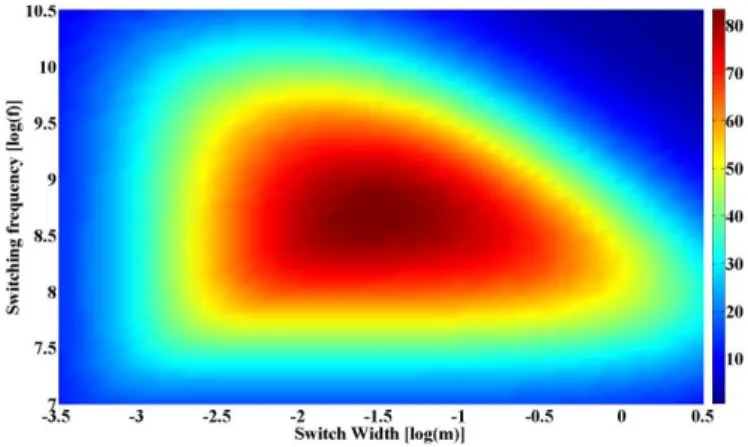
Fig. 3 shows the efficiency versus the two design variables {W,F} for a typical CMOS case: λq=1fC/µm, λr=1kΩ×µm, Ro=1Ω, σ=10nF/mm2, α=1%, and S=1mm2. This graph clearly shows an optimal point {Wopt,Fopt} where the power efficiency is maximized. Here, the optimal width and switching frequency are 31600µm and 500MHz, respectively.
Fig. 3. SCC efficiency v. the two main design variables {W,F}
III. KEY TECHNOLOGY PARAMETERS FOR SCC
As shown in equation (6), the losses are directly related to four critical technological parameters. In this section, the test bench to extract each parameter from a targeted CMOS technology is described in detail.
A. Parameter Extraction for Switch Properties
The losses due to the switches are mainly evaluated by the on-state resistance density (λr) and the gate charge density (λq) in the modeling presented in equation (2). These two parameters are extracted using the schematic given in Fig.4. The on-state current through drain-source transistor is set by the resistance R following the relation Ids = (Vin-Vds)/R under ohmic regime condition. The drain-source voltage is less than 100mV and Vgs is maximized to maintain the transistor in the
ohmic region. The Rdriver value is set to maintain the rise time of the gate voltage Vg inferior to the switching period Tsw.
Fig. 4. Schematic for the extraction of the on-state resitance density and the gate charge density
In order to reduce the on-state resistor, the length of the transistor Lsw is minimized while the voltage rating is ensured. Using DC analysis, the parameter λr is evaluated thanks to the Vd potential when the switch is in on-state so that:
𝜆
𝑟= 𝑅𝑂𝑁× 𝑊 =𝑉𝑑
𝑉𝑖𝑛− 𝑉𝑑× 𝑅 × 𝑊 (7)
By using a transient analysis, the parameter λq is extracted
as a result of the energy delivered by the driver to the gate of the transistor during one switching period. Thus, the charge density λq is given by:
𝜆𝑞= 𝐸𝐷𝑟𝑖𝑣𝑒𝑟 𝑉𝐼𝑁𝑊 = 1 𝑊∫ 𝑖𝑑𝑟𝑖𝑣𝑒𝑟(𝑡)𝑑𝑡 𝑇𝑠𝑤 𝑡=0 (8) B. Parameter Extraction for Flying Capacitor Properties
To simplify the capacitor extraction from the complex model given by a technological design kit, we assume the flying capacitor terminals {Vc+,Vc-} are only connected to the bulk by pure capacitors Ctop and Cbot as shown in Fig. 5.a. The extraction of α and σ is done by performing an AC analysis and adding resistance Rm connected as shown in Fig. 5.b. Due to the poly-type capacitor structure [6], only Cbot is evaluated because Ctop is negligible most of the time.
Fig. 5. (a) Equivalent schematic of a flying capacitor and (b) Schematic for the extraction of the capacity density and the parasitic capacity
For MIM and TSC, the Ctop and Cbot parasitic capacitors are negligible compared to Cfly by their nature. The equivalent impedance seen by the AC source can be expressed as:
𝑍𝑒𝑞(𝑠) =
1 + 𝑅𝑚(𝐶𝑓𝑙𝑦+ 𝐶𝑏𝑜𝑡)𝑠
(1 + 𝑅𝑚𝐶𝑏𝑜𝑡𝑠)𝐶𝑓𝑙𝑦𝑠 (9)
This equation leads to two cutoff frequencies in the AC analysis which directly determine the Cfly and Cbot capacitor values by the following expressions:
𝐶𝑏𝑜𝑡 =2𝜋𝑅1
𝑚𝐹𝑐1 and 𝐶𝑓𝑙𝑦=
1
2𝜋𝑅𝑚𝐹𝑐2− 𝐶𝑏𝑜𝑡 (10) Then, from (10), α and σ values are given by the following equations:
∝=𝐶𝑏𝑜𝑡
𝐶 and 𝜎 = 𝐶
𝑆 (11) C. Key Parameters for Major Technology Nodes
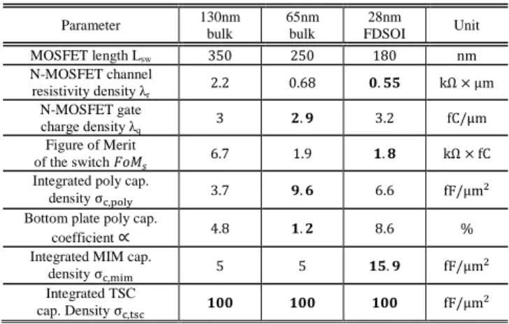
Using the above extraction procedure, Table 1 gives the most important technological parameters to assess the capacity of achieving the highest efficiency in three widely-used CMOS technologies. The best parameters are highlighted in bold. To be able to work with 1.8V, the transistors have thick oxides. This means that the minimal length for the switch is greater than the minimal length allowed by the process. We therefore assume that TSC geometry density is independent of the technology node [31]. The equivalent serial resistor (ESR) is also not taken into account.
The classical factor of merit, FoMs = RonQg, equal to the product of λr and λq, gives a trend of how close the transistor will be to an ideal switch. Here, the 28nm and 65nm nodes have similar values leading to less transistor contribution on the overall loss expressed in (6), than the 130nm node. The 65nm node has the best poly-type capacitor density with lowest parasitic capacitor ratio. These two facts show that scaling does not necessarily provide better technological parameters to achieve the highest power efficiency. On the other hand, the MIM-option which is not directly linked to a scaling effect provides better capacitor density but needs additional layers leading to extra silicon cost.
TABLEI
PROCESS PARAMETERS INFLUENCING CONVERTER PERFORMANCE
Parameter 130nm bulk 65nm bulk 28nm FDSOI Unit MOSFET length Lsw 350 250 180 nm N-MOSFET channel resistivity density λr 2.2 0.68 𝟎. 𝟓𝟓 kΩ × μm N-MOSFET gate charge density λq 3 𝟐. 𝟗 3.2 fC/μm Figure of Merit of the switch 𝐹𝑜𝑀𝑠 6.7 1.9 𝟏. 𝟖 kΩ × fC
Integrated poly cap.
density σc,poly 3.7 𝟗. 𝟔 6.6 fF/μm
2
Bottom plate poly cap.
coefficient ∝ 4.8 𝟏. 𝟐 8.6 % Integrated MIM cap.
density σc,mim 5 5 𝟏𝟓. 𝟗 fF/μm
2
Integrated TSC
cap. Density σc,tsc 𝟏𝟎𝟎 𝟏𝟎𝟎 𝟏𝟎𝟎 fF/μm 2
Note: in bold, the best benefit value in terms of converter design (1) Thick oxide 150nm- and 280nm-long channel transistors in 65 and 28nm technology, respectively; driving voltage 1.8V; (2) Thick oxide polysilicon capacitors at 1.0V bias with 1.8V maximal voltage rating; (3) additional layers needed for MIM (Metal Insulator Metal) capacitor option, the bottom plate of the MIM is negligible. In 28nm, the MIM voltage rating is 1.1V (4) included in the DKit model (not post-layout extracted).
IV. ACHIEVABLE SCCPOWER DENSITY
A. Optimization Procedure
The aim of the optimization is to find the highest efficiency for a silicon surface in a 0.1 to 50mm² range. For each given surface S, the capacitor density and chosen capacitor type determine the Cfly value. Then, the design freedom couple {Wopt,Fopt} is determined by using expressions (3) and (6) in an exhaustive search procedure. After that, we perform a transistor-level simulation to find a more precise couple value. Lastly, the Po/S ratio is calculated to give the power density at each given surface.
B. Efficiency v. Power Density
Fig. 6 shows the evolution of the efficiency against power density for each capacitor type available in 28nm FDSOI technology. This figure shows the strong influence of the capacitor density and the parasitic capacitance on power efficiency. As the TSC has the better density, as shown in Table 1, the best efficiency is achieved by this capacitor type. The poly-type capacitor has the lowest efficiency due to its low density and high parasitic capacitance ratio α. Another example from Fig. 6 is that using the power density of a converter with TSC is five times better than using the MIM option to reach 80% efficiency.
Fig. 6. Influence of the capacitors for the 28nm technology
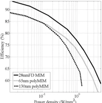
Fig. 7 shows the efficiency v. power density in the 28nm, 65nm and 130nm technologies for the same capacitor type i.e. TSC in order to only show the RonQg impact. Due to the similar RonQg FoMs, see Table 1, the 28 and 65nm nodes achieve similar efficiency. These results show that the thinner node does not necessarily improve the converter performance for the same capacitor density. On the other hand, the 130nm process has the lowest power density because its FoMs is three times greater than the other technologies. Beyond the length, RonQg characterization is needed to determine the technology ability to propose efficient switching properties. Notice the most
recent technologies limit the voltage rating capability of the transistor, thus limiting the input voltage value.
Fig. 7. Influence of the node technology for the TSC capacitors
The evolution of the efficiency against power density for each technology using the available capacitor i.e. a stack of MIM- and poly-types is shown in Fig. 8. Due to the highest MIM capacitor density, the 28nm technology has the best efficiency for any power density. Despite a better RonQg, the 65nm node gives a similar efficiency to the 130nm one which leads to the conclusion than the capacitance density is the predominant technology parameter.
Fig. 8. Influence of the node technology for the MIM- and poly-type capacitors
V. CONCLUSION
In this paper, we have studied the impact of CMOS scaling on the fully-integrated capacitor-based converter. We have
proposed a compact modeling to highlight the most critical technology parameters which influence the power efficiency. In addition, we have described the procedure to extract these parameters. By using the optimization process based on the proposed models and transistor-level simulation, we have studied three CMOS technological nodes 130, 65 and 28nm. As shown in the simulation results, the capacitor density is the most critical parameter for achieving high power density conversion. Due to the high MIM density in the studied 28nm node, which is not directly linked to the scaling effect, this technology offers the best power density for 1.8V input voltage.
REFERENCES
[1] I. Miro-Panades, A Fine Grain Variation-Aware Dynamic Vdd-Hopping AVFS Architecture on a 32nm GALS MPSoC, IEEE Journal of
Solid-State Circuits, vol.49, no.7, pp.1475-1486, 2014
[2] A. Todri, M. Marek-Sadowska, Power Delivery for Multi-Core Systems,
IEEE Transactions on Very Large Scale Integration Systems, vol.19,
no.12, pp.2243-2255, 2011.
[3] G. Mouslih, A. Todri-Sanial, P. Nouet, On analysis of on-chip DC-DC converters for power delivery networks, IEEE International Symposium
on VLSI (ISVLSI), pp.557-560, 2015.
[4] C. R. Sullivan, D. V. Harburg, J. Qiu, C. G. Levey, and D. Yao, “Integrating Magnetics for On-Chip Power: A Perspective,” IEEE
Transactions on Power Electronics, vol. 28, no. 9, pp. 4342–4353, Sep.
2013.
[5] S. R. Sanders, E. Alon, H.-P. Le, M. D. Seeman, M. John, and V. W. Ng, “The Road to Fully Integrated DC-DC Conversion via the Switched-Capacitor Approach,” IEEE Transactions on Power Electronics, vol. 28, no. 9, pp. 4146–4155, Sep. 2013.
[6] E. A. Burton, G. Schrom, F. Paillet, J. Douglas, W. J. Lambert, K. Radhakrishnan, and M. J. Hill, “FIVR - Fully integrated voltage regulators on 4th generation Intel Core SoCs,” in 2014 Twenty-Ninth
Annual IEEE Applied Power Electronics Conference and Exposition (APEC), 2014, pp. 432–439.
[7] J. Wibben and R. Harjani, “A High-Efficiency DC-DC Converter Using 2 nH Integrated Inductors,” IEEE Journal of Solid-State Circuits, vol. 43, no. 4, pp. 844–854, Apr. 2008
[8] Y. K. Ramadass, A. A. Fayed, and A. P. Chandrakasan, “A Fully-Integrated Switched-Capacitor Step-Down DC-DC Converter With Digital Capacitance Modulation in 45 nm CMOS,” IEEE Journal of
Solid-State Circuits, vol. 45, no. 12, pp. 2557–2565, Dec. 2010.
[9] B. Maity and P. Mandal, “A High Performance Switched Capacitor-Based DC-DC Buck Converter Suitable for Embedded Power Management Applications,” IEEE Transactions on Very Large Scale
Integration (VLSI) Systems, vol. 20, no. 10, pp. 1880–1885, Oct. 2012.
[10] L. Su, D. Ma, and A. P. Brokaw, “Design and Analysis of Monolithic Step-Down SC Power Converter With Subthreshold DPWM Control for Self-Powered Wireless Sensors,” IEEE Transactions on Circuits and
Systems I: Regular Papers, vol. 57, no. 1, pp. 280–290, Jan. 2010.
[11] A. K. P. Viraj and G. A. J. Amaratunga, “A Monolithic CMOS 5V/1V Switched Capacitor DC-DC Step-down Converter,” in IEEE Power
Electronics Specialists Conference, 2007. PESC 2007, 2007, pp. 2510–
2514.
[12] G. Patounakis, Y. W. Li, and K. L. Shepard, “A Fully Integrated On-Chip DC-DC Conversion and Power Management System,” IEEE
Journal of Solid-State Circuits, vol. 39, no. 3, pp. 443–451, Mar. 2004.
[13] L. G. Salem and P. P. Mercier, “A 45-ratio recursively sliced series-parallel switched-capacitor DC-DC converter achieving 86% efficiency,” in Custom Integrated Circuits Conference (CICC), 2014 IEEE Proceedings of the, 2014, pp. 1–4.
[14] R. Jain, B. M. Geuskens, S. T. Kim, M. M. Khellah, J. Kulkarni, J. W. Tschanz, and V. De, “A 0.45-1 V Fully-Integrated Distributed Switched Capacitor DC-DC Converter With High Density MIM Capacitor in 22 nm Tri-Gate CMOS,” IEEE Journal of Solid-State Circuits, vol. 49, no. 4, pp. 917–927, Apr. 2014.
[15] A. Biswas, Y. Sinangil, and A. P. Chandrakasan, “A 28 nm FDSOI Integrated Reconfigurable Switched-Capacitor Based Step-Up DC-DC Converter With 88% Peak Efficiency,” IEEE Journal of Solid-State
Circuits, vol. PP, no. 99, pp. 1–10, 2015.
[16] L. Chang, R. K. Montoye, B. L. Ji, A. J. Weger, K. G. Stawiasz, and R. H. Dennard, “A fully-integrated switched-capacitor 2 #x2236;1 voltage converter with regulation capability and 90% efficiency at 2.3A/mm2,” in IEEE Symposium on VLSI Circuits (VLSIC), 2010, pp. 55–56. [17] D. Somasekhar, B. Srinivasan, G. Pandya, F. Hamzaoglu, M. Khellah, T.
Karnik, and K. Zhang, “Multi-Phase 1 GHz Voltage Doubler Charge Pump in 32 nm Logic Process,” IEEE Journal of Solid-State Circuits, vol. 45, no. 4, pp. 751–758, Apr. 2010.
[18] T. Van Breussegem and M. Steyaert, “A 82% efficiency 0.5% ripple 16-phase fully integrated capacitive voltage doubler,” in Proceedings of the
Symposium on VLSI Circuits, 2009, pp. 198–199.
[19] H.-P. Le, S. R. Sanders, and E. Alon, “Design Techniques for Fully Integrated Switched-Capacitor DC-DC Converters,” IEEE Journal of
Solid-State Circuits, vol. 46, no. 9, pp. 2120–2131, Sep. 2011
[20] D. Somasekhar, B. Srinivasan, G. Pandya, F. Hamzaoglu, M. Khellah, T. Karnik, and K. Zhang, “Multi-phase 1GHz voltage doubler charge-pump in 32nm logic process,” in Symposium on VLSI Circuits, 2009, pp. 196– 197.
[21] Y. K. Ramadass and A. P. Chandrakasan, “Voltage scalable switched capacitor DC-DC converter for ultra-low-power on-chip applications,” in Power Electronics Specialists Conference, 2007, pp. 2353–2359. [22] T. M. Andersen, F. Krismer, J. W. Kolar, T. Toifl, C. Menolfi, L. Kull,
T. Morf, M. Kossel, M. Brandli, P. Buchmann, and others, “A deep trench capacitor based 2: 1 and 3: 2 reconfigurable on-chip switched capacitor DC-DC converter in 32 nm SOI CMOS,” in Applied Power
Electronics Conference and Exposition (APEC), 2014, pp. 1448–1455.
[23] G. V. Pique, “A 41-phase switched-capacitor power converter with 3.8mV output ripple and 81% efficiency in baseline 90nm CMOS,” in
Solid-State Circuits Conference Digest of Technical Papers (ISSCC),
2012, pp. 98–100.
[24] T. Souvignet, B. Allard, S. Trochut, A fully integrated switched-capacitor regulator with frequency modulation control in 28nm FDSOI,
IEEE Transactions on Power Electronics, in press, 2016.
[25] G. Pillonnet, N. Jeanniot and P. Vivet “3D ICs: An Opportunity for Fully Integrated, Dense and Efficient Power Supplies,” in IEEE int. conference on 3DIC, 2015
[26] Y. Pascal, and G. Pillonnet, “Efficiency comparison of capacitor-, inductor- and resonant-based converters fully integrated in CMOS technology,” Journal of Emerging and Selected Topics in Circuits and
Systems, Sept. 2015, in press.
[27] J. Gjanci and M. H. Chowdhury, “A Hybrid Scheme for On-Chip Voltage Regulation in System-On-a-Chip (SOC),” IEEE Transactions
on Very Large Scale Integration (VLSI) Systems, vol. 19, no. 11, pp.
1949–1959, Nov. 2011.
[28] M. S. Makowski, “A canonical switched capacitor DC-DC converter,” in
15th Workshop on Control and Modeling for Power Electronics (COMPEL), 2014, pp. 1–8.
[29] M. S. Makowski and D. Maksimovic, “Performance limits of switched-capacitor DC-DC converters,” in 26th Annual IEEE Power Electronics
Specialists Conference, 1995, vol. 2, pp. 1215–1221.
[30] S. Ben-Yaakov, “Behavioral Average Modeling and Equivalent Circuit Simulation of Switched Capacitors Converters,” IEEE Transactions on
Power Electronics, vol. 27, no. 2, pp. 632-636, Feb. 2012.
[31] O. Guiller, S. Joblot, Y. Lamy, A. Farcy, E. Defay, and K. Dieng, “Through Silicon Capacitor co-integrated with TSV as an efficient 3D decoupling capacitor solution for power management on silicon interposer,” in 64th IEEE Electronic Components and Technology