HAL Id: hal-03015743
https://hal.archives-ouvertes.fr/hal-03015743
Submitted on 25 Nov 2020
HAL is a multi-disciplinary open access
archive for the deposit and dissemination of
sci-entific research documents, whether they are
pub-lished or not. The documents may come from
teaching and research institutions in France or
abroad, or from public or private research centers.
L’archive ouverte pluridisciplinaire HAL, est
destinée au dépôt et à la diffusion de documents
scientifiques de niveau recherche, publiés ou non,
émanant des établissements d’enseignement et de
recherche français ou étrangers, des laboratoires
publics ou privés.
Study of resonant transport in InAs-based quantum hot
electron transistors
H. Nguyen Van, A. Baranov, R. Teissier, M. Zaknoune
To cite this version:
H. Nguyen Van, A. Baranov, R. Teissier, M. Zaknoune. Study of resonant transport in InAs-based
quantum hot electron transistors. AIP Advances, American Institute of Physics- AIP Publishing LLC,
2020, 10 (7), pp.075027. �10.1063/5.0011780�. �hal-03015743�
quantum hot electron transistors
Cite as: AIP Advances 10, 075027 (2020); https://doi.org/10.1063/5.0011780Submitted: 24 April 2020 . Accepted: 03 July 2020 . Published Online: 30 July 2020
H. Nguyen Van, A. N. Baranov, R. Teissier, and M. Zaknoune COLLECTIONS
Paper published as part of the special topic on Chemical Physics, Energy, Fluids and Plasmas, Materials Science
and Mathematical Physics
ARTICLES YOU MAY BE INTERESTED IN
Chalcogen-hyperdoped germanium for short-wavelength infrared photodetection
AIP Advances 10, 075028 (2020);
https://doi.org/10.1063/5.0008281
Deep ultraviolet hyperspectral cryomicroscopy in boron nitride: Photoluminescence in
crystals with an ultra-low defect density
AIP Advances 10, 075025 (2020);
https://doi.org/10.1063/5.0013121
Effect of post-deposition treatment on electrical properties of solution-processed a-IGZO
Schottky diodes
AIP Advances
ARTICLE scitation.org/journal/advStudy of resonant transport in InAs-based
quantum hot electron transistors
Cite as: AIP Advances 10, 075027 (2020);doi: 10.1063/5.0011780
Submitted: 24 April 2020 • Accepted: 3 July 2020 • Published Online: 30 July 2020
H. Nguyen Van,1,a) A. N. Baranov,1 R. Teissier,1 and M. Zaknoune2 AFFILIATIONS
1Institut d’Electronique du Sud, CNRS/Univ. Montpellier 2, Montpellier, France
2Institut d’Electronique de Microélectronique et de Nanotechnologie, CNRS/Univ. Lille 1, Villeneuve d’Ascq, France a)
Authors to whom correspondence should be addressed:[email protected]
ABSTRACT
A study of transport in a quantum hot electron transistor made of an InAs/AlSb heterostructure is reported. It exhibited that the quantum hot electron transistors with a thick emitter efficiently prevented the parasitic base currents compared with transistors with a thin emitter. The static characteristics of the fabricated devices demonstrated an enhancement of the current gain of 9 and a collector breakdown voltage of 1.5 V with thick-emitter designed transistors. In optimized devices, the current is dominated by fast resonant tunneling that is promising for their future development of as high frequency transistors.
© 2020 Author(s). All article content, except where otherwise noted, is licensed under a Creative Commons Attribution (CC BY) license (http://creativecommons.org/licenses/by/4.0/).https://doi.org/10.1063/5.0011780., s
I. INTRODUCTION
Very high frequency electronic devices are essential for high speed telecommunications or sub-mm wave generation and detec-tion systems. The performance of high frequency transistors is strongly related to the intrinsic transport properties of the used semiconductors. As a matter of fact, heterojunction bipolar tran-sistors (HBTs) made of an InGaAs lattice matched on the InP sub-strate have significantly better frequency response as compared to GaAs-based devices.1Furthermore, a significant increase in the cut-off frequencyft exceeding 700 GHz has been obtained thanks to the use of the indium-rich strained InGaAs material.2 Going far-ther in this direction, smaller bandgap materials such as InAs and InSb are attractive candidates for even more rapid devices.3In par-ticular, electrons in InAs have a saturation velocity and mobility twice the values of InGaAs or InP. The work presented here aims to take benefit from these favorable properties of InAs-based struc-tures to overcome the existing limits of electron transport in HBTs. InAs has already been proposed as a good material for bipolar tran-sistors,4,5but its use in HBTs was hampered by the lack of a large bandgap material, a lattice matched on the InAs substrate, that could provide the large valence band offset required for npn HBTs. A
novel design of the transistor was proposed to overcome the cur-rent limitations above. This device that we call quantum hot elec-tron transistor (QHET) is a unipolar transistor using the concept of a hot electron transistor (HET).6–8However, unlike the previously reported HET,9–11it relies on a coherent vertical transport in a multi-quantum well InAs/AlSb heterostructure similar to that of multi-quantum cascade lasers.12It is not dependent on valence band offset align-ments since only electrons in the conduction band are involved. For these reasons, its first advantage overnpn HBTs is the high base sheet conductance,6,13accessible with moderate n-type doping levels (typ-ically n ∼ 1018cm−3as compared to p ∼ 1020cm−3in HBTs), which is a key parameter for high speed operation. Second, electron trans-port in the short (typically 100 nm–200 nm) bulk InAs collector is mostly ballistic with calculated transit times much shorter than those in InP-based devices thanks to the larger saturation velocity.14It also revealed that the InAs-based QHET with a submicronic footprint of the emitter exhibited low base resistance, high-current densi-ties, and low operating voltage. Furthermore, the InAs-based QHET yielded the promising cut-off frequency of 77 GHz at room tempera-ture for the first time.6With the primary results, InAs-QHETs have been demonstrated to extend the frequency limit of vertical trans-port transistors toward the THz range.6 However, the physics of
AIP Advances 10, 075027 (2020); doi: 10.1063/5.0011780 10, 075027-1
transport of these devices are still unexploited, which is a necessary factor to continuously optimize the transistor structures as well as gain the dynamic performance.
In this Letter, we study the physics of transport in an original high speed vertical transport transistor based on InAs. To evaluate the physics of transport of InAs-based QHET, two QHET struc-tures with different emitter designs have been fabricated and studied at cryogenic temperatures and room temperature. It demonstrated that the emitter with a thick barrier is sufficient to prevent the leak-age currents from the emitters, which efficiently enhanced the gain statics.
II. EXPERIMENT
A. Design of QHET structures
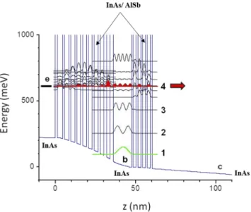
The electron transport in the active part of the QHET is con-trolled by the quantum design of electron sub-bands. The complete layer structure, device geometry, and the conduction band diagram of the active part of the device are presented inFigs. 1and2. InFig. 2, the band structure of the multi-quantum well part of the device is calculated using a home-made Schrödinger–Poisson solver based on the transfer matrix method. In order to account for the non-uniform electric field, each individual layer of the heterostructure was dis-cretized in ten sections with a constant potential. We considered in the calculation of the energy levels and wavefunctions that the first and last AlSb barriers were infinitely thick. The boundary con-ditions for the electric field (F) were F = 0 kV/cm on the emitter side and F = 10 kV/cm on the collector side. Finally, we assumed that the electrons were distributed with independent thermal
distributions in the emitter superlattice and in the base layer. The potential drop between the two associated Fermi levels corre-sponded to the junction biasVBE= 0.45 V. The material parameters used in the calculation are given in Ref.15.
The base is made of a n-type InAs quantum well (QW) doped with silicon to 1018cm−3. With a typical electron mobility greater than 104cm2/V/s, it corresponds to a base sheet resistance lower than 500 Ω/◽. The emitter–base junction and collector barrier con-sist of graded InAs/AlSb superlattices. The collector transit region is made of 200 nm-thick undoped InAs. When compared to quan-tum cascade laser (QCL), the major difference in the band structure is the position of the extraction miniband that is resonant with the upper state of the active QW (the base of transistor) instead of the lower state in a QCL. Majority electrons provided by the doping in the base are confined in the QW ground state thanks to the collector barrier. When the QHET is supplied with suitable emitter–base bias (VBE), electrons transit from the emitter to the collector (currentIC) through the coherent transport via the QW excited state that is res-onantly coupled with the emitter and collector barrier states (Level 4, corresponding to the solid wavefunction inFig. 2) and are trans-ferred to the high field region of the base–collector junction made of bulk InAs. This resonant state is coupled to the continuum of states in the bulk collector; hence, the transit time of electrons through the base should be close to their dephasing time, typically a few tens of femtoseconds. The fraction of electrons scattered down to the lower states in the base produces the base currentIB. An additional parasitic base current may arise from the direct injection from the emitter to the lower state of the base. Two samples were designed to observe the parasitic base currents. Herein, sample H5 contained thinner barriers in the emitter, which was reported in the previous
FIG. 1. (a) Layer sequence of the studied structures. (b) Schematic geometry of the studied double-mesa devices. (c) Optical micrograph of a fabricated QHET using
AIP Advances
ARTICLE scitation.org/journal/advFIG. 2. Calculated conduction band diagram of the active part of the device, when
biased in resonant condition (VBE = 0.45 V). The quantized energy levels and
wavefunctions are represented. Under normal operation, a resonant electron cur-rent flows from the emitter Fermi level (e) through the fourth quantized state (solid wavefunction) of the base and propagates ballistically in the collector.
paper.6 A new structure called sample H2 was designed with the thicker barriers in the emitter compared with that of sample H5. The exact layer sequence is given inFig. 1. The reduced barrier thickness resulted in a stronger coupling of the emitter states with the base quantized states. A quantitative estimation of this coupling is given by the level splitting at resonance (2hΩ) between the injector and the fourth base state. We calculated a value of 2hΩ = 11 meV for sample H2 and 2hΩ = 45 meV for sample H5. The strong coupling in H5, obtained with 1 nm-thick AlSb barriers was intended to provide a large emitter current density (JE) at resonance. This is an important parameter for high frequency operation: using the common analysis of high frequency response in HBTs, the increase of emitter current density directly impacts the cutoff frequency through the reduction of the emitter differential resistance and subsequently the junction charging times, as described in Ref.6. However, we estimate that the tunneling efficiency in the new structure is still large enough to allow the injection of very high current densities, greater than 500 kA/cm2.
B. Fabrication of QHET
The samples were grown by molecular beam epitaxy on the InAs substrate, using a Riber Compact 21 solid source machine equipped with As and Sb valved cracking cells. Thanks to the exper-tise that we developed for many years in the growth of InAs/AlSb QCLs,11,14 state of the art heterostructures were available for this work. From the grown wafers, QHETs were formed by a double-mesa processing that produced 10 × 10 μm2emitter and 20 × 30 μm2base mesas (Fig. 1). Ohmic contacts were made of nonalloyed Cr/Au. In this device fabrication, the critical step was the accurate contact of the thin base. A high precision layer-by-layer selective wet
etching process has been developed for this purpose.6The devices were passivated using a hard-backed resist that also supported the contact pads of the emitter and the base. The collector contact was directly made on the n-doped InAs substrate.
III. RESULTS AND DISCUSSION
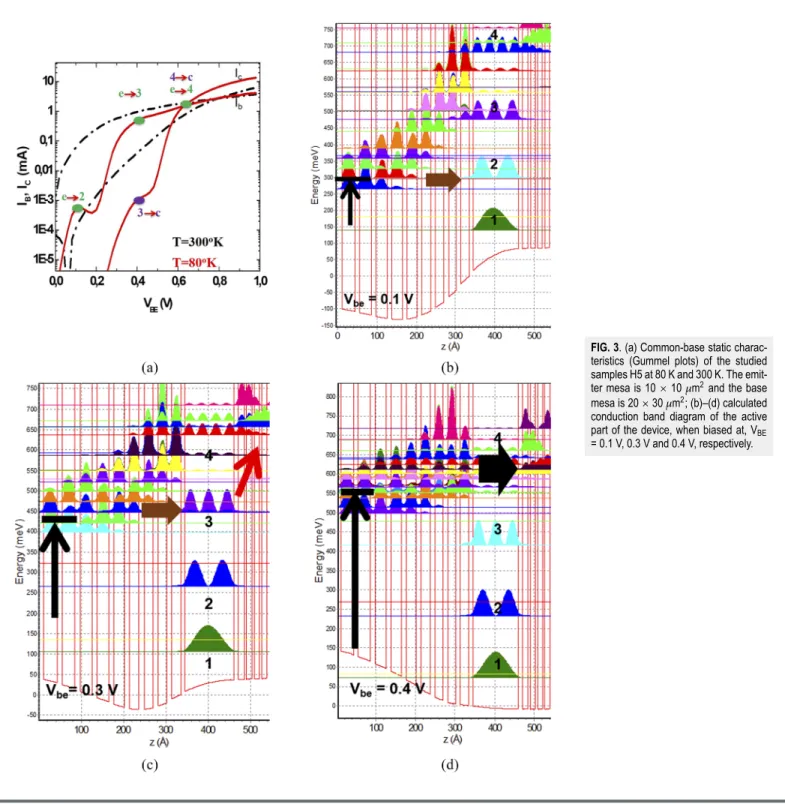
Figure 3shows the common base characteristics (Gummel plot) of QHETs from H5 structures at room temperature and cryogenic temperature (80 K). The Gummel plot displays the currentsIBand IC as a function ofVBE, for a constant base–collector bias (VBC = 0). The curves measured at the low temperatures give useful infor-mation to understand the origin of the measured currents in the different bias ranges. On sample H5, one can see three resonances in the base current similar to what is observed in a more conventional resonant tunneling diode (solid green circle), which are represented as (e → 2), (e → 3), and (e → 4) inFig. 3(a). They correspond to the successive alignments of the emitter Fermi level with the base QW Levels 2, 3, and 4, whileVBEis biased at 0.1 V, 0.3 V, and 0.4 V [Figs. 3(b)–3(d), respectively]. In the meantime, there are also suc-cessive alignment of base QW Levels 3 and 4 with collector Fermi levels, which are known as (3 → c), and (4 → c), respectively. When the fourth state of the base enters in resonance with the emitter and the collector, the expected current density is very high (larger than 500 kA/cm2). In the present study, the large size of the emitter mesa and the device geometry did not allow reaching such high currents, notably because of the base access resistance, as shown in Ref.6. As a consequence, the (e → 4) resonance is only observed as an increase in the collector current limited by the access resistance. In addition, the real potential drop in the emitter–base junction is significantly lower than the appliedVBE bias. A significant collector current is only measured when electrons are injected directly into Level 4, i.e., forVBE>0.6 V since it is the only level that is coupled to the col-lector. Nevertheless, a small escape current can be seen from the electron injected into Level 3 at a biasVBE ∼0.4 V (solid purple circle). Hence, the base current measured forVBE<0.6 V appears to be mostly a parasitic current injected directly from the emitter to the three lower base states. At room temperature, these resonances are not visible since they are broadened by thermal activation. One can, however, conclude that the strong base current measured below 0.6 V also originates from the same parasitic channels. In the same way, the large ideality factor of currentIc is due to the current flow-ing from Level 3 to the collector at low biasVBE. For sample H5, the current gain (i.e.,IC>IB) is only observed whenVBE>0.8 V. The static gain β = IC/IB reaches a maximum value of 5 at large bias.
Sample H2 has been designed in order to reduce the parasitic current observed in sample H5. This has been done by reducing the emitter–base coupling thanks to the thicker AlSb barrier in the end of the emitter superlattice, as already explained, and also by adjust-ing the alignment of the levels originatadjust-ing from the last emitter QWs with the Level 4 of the base. At low temperatures, one can still see the resonance e → 3 forVBE∼0.4 V, but this parasitic current has been reduced by three orders of magnitudes as compared to sample H5 [Fig. 4(a)]. The currents in the QHET H2 are then dominated by the currents flowing through the resonant Level 4, as ideally wanted [Fig. 4(b)]. At room temperature, the Gummel plot of transistors H2
AIP Advances 10, 075027 (2020); doi: 10.1063/5.0011780 10, 075027-3
demonstrated a current gain forVBE>0.3 V with a maximal value of β = 9.
In resonant conditions, the current gain can be seen as the ratio of the inter-sub-band relaxation time τrelin the base to the transit time τtrfor electrons in the resonant state,7
β = τrel τtr
. (1)
The time τrelcan be estimated by the calculated LO phonon scat-tering rates from Level 4 to the three lower levels. We obtained a value of τrel= 0.7 ps. However, this is a probably overestimated value since additional scattering mechanisms, such as interface roughness or electron–electron scattering may play a significant role. We esti-mate that electron–electron scattering is still limited thanks to the relatively low doping level of the base. We can derive base transit
FIG. 3. (a) Common-base static
charac-teristics (Gummel plots) of the studied samples H5 at 80 K and 300 K. The emit-ter mesa is 10 × 10μm2and the base
mesa is 20 × 30μm2; (b)–(d) calculated
conduction band diagram of the active part of the device, when biased at, VBE
AIP Advances
ARTICLE scitation.org/journal/advFIG. 4. (a) Common-base static
charac-teristics (Gummel plots) of the studied samples H2 at 80 K and 300 K. The emit-ter mesa is 10 × 10μm2and the base
mesa is 20 × 30μm2; (b) calculated
con-duction band diagram of the active part of the device, with thick barrier layers for reducing the parasitic currents.
time tBby converting the equation above, tB≈τtr=τrel
β . (2)
From the measured gain β = 9, we can conclude that the transit time for resonant tunneling is tB= τrel/β < 78 fs. This analysis indi-cates the future directions to explore in order to further increase the current gain in a QHET structure: reduce the extraction time with a more transparent collector barrier or increase the inter-sub-band relaxation time with a different base QW design. The base resistance is estimated to be about 350 Ω–500 Ω, extracted from the Gummel plot for both structures of H2 and H5. Evidently, this value, due
FIG. 5. Common-emitter static characteristics Ic(Vce) of sample H2 at 80 K and
300 K. The successive traces correspond to base currents increasing from 0 mA to 3 mA in 0.5 mA steps.
to the large dimension of the devices, is not suitable for high fre-quency operation that would require submicron dimensions and a large aspect ratio of the emitter mesa.
The static common-emitter output characteristics Ic(Vce) of QHET H2, measured at both cryogenic and room temperatures, are shown inFig. 5. A clear saturation of currentIc is obtained with a differential current gain of about 9, consistent with the value of β measured in common-base configuration. The threshold voltage is 0.5 V and collector breakdown voltage BVCE0 is larger than 1.5 V. However, it must be noted that these values are probably overesti-mated because of the parasitic series resistances due to the geometry of the device. The relatively high access resistances also limited the maximum current density to JE ≈30 kA/cm2. Low values of the breakdown voltage were often presented as the major drawback of low bandgap materials, such as InAs. The data of Fig. 5 demon-strate that good operating conditions can nevertheless be obtained in the QHETs. Under operating conditions, the voltage drop across the bulk InAs collector transit region is approximately equal toVCE −0.6 V (see the band diagram onFig. 2). Hence, the breakdown starts when the voltage applied to the collector junction is about 0.9 V. It corresponds to an electric field of 45 kV/cm in the 200 nm-thick collector, which is a sensible value. The two characteristics at low and room temperature are quite similar, as expected for a device in which transport is mainly controlled by resonant tunneling. A noteworthy difference is, however, the stronger collector leakage current at room temperature as seen on the lower curve (IB = 0). This is explained by the thermally activated transport of electrons from the base ground state to the collector barrier miniband.
IV. CONCLUSIONS
In summary, we demonstrated the feasibility of the novel ver-tical transport QHETs based on InAs. A suitable current gain and operating voltages are obtained under static operation. Electron transport is shown to be controlled by potentially very fast coher-ent resonant tunneling through the base excited state. Together with
AIP Advances 10, 075027 (2020); doi: 10.1063/5.0011780 10, 075027-5
previously reported very short theoretical collector transit times14 and excellent experimental base sheet resistance,6,13this study pro-vides an additional evidence that the QHET technology has all required properties for producing a transistor with cut-off fre-quencies in the THz range. The future steps toward the demon-stration of high speed operation are, first, to optimize the tran-sistor structures to enhance the static gain and, second, use a metamorphic growth on semi-insulating GaAs4 in order to allow
high frequency characterizations. The improved design proposed here should result in a significantly better emitter differential resis-tance and, hence, improve the cutoff frequencies as compared to Ref.6.
ACKNOWLEDGMENTS
The authors thank the support of French Agence Nationale de la Recherche under the program TACHUS2 (Grant No. ANR-08-BLANC-0299).
DATA AVAILABILITY
The data that support the findings of this study are available from the corresponding author upon reasonable request.
REFERENCES
1Z. Griffith, M. J. W. Rodwell, X.-M. Fang, D. Loubychev, Y. Wu, J. M.
Fas-tenau, and A. W. K. Liu, “InGaAs/InP DHBTs with 120-nm collector having simultaneously hight ft, fmax≥450 GHz,”IEEE Electron Device Lett.26, 530–532 (2005).
2
W. Hafez, W. Snodgrass, and M. Feng, “12.5 nm base pseudomorphic hetero-junction bipolar transistors achieving ft= 710 GHz and fmax= 340 GHz,”Appl.
Phys. Lett.87, 252109 (2005).
3
B. R. Bennett, R. Magno, J. B. Boos, W. Kruppa, and M. G. Ancona, “Animonide-based compound semiconductors for electronic devices,”Solid-State Electron.49, 1875 (2005).
4
K. L. Averett, X. Wu, M. W. Koch, and G. W. Wicks, “Low-voltage InAsP/InAs HBT and metamorphic InAs BJT devices grown by molecular beam epitaxy,”
J. Cryst. Growth251, 852 (2003).
5
P. D. Moran, D. Chow, A. Hunter, and T. F. Kuech, “Fabrication of InAs/AlSb/GaSb heterojunction bipolar transistors on Al2O3substrates by wafer
bonding,”Appl. Phys. Lett.78, 2232 (2001).
6
H. Nguyen van, J. C. Moreno, A. N. Baranov, R. Teissier, and M. Zaknoune, “Sub-micrometer process and RF operation of InAs quantum hot-electron transistors,”
IEEE Electron Device Lett.33(6), 797 (2012).
7
T. Daoud, G. Boissier, J. Devenson, A. N. Baranov, and R. Teissier, “Experimental study of transport in InAs quantum hot electron transistor,”J. Phys.: Conf. Ser. 193, 012014 (2009).
8
M. Heiblum, “Tunneling hot electron transfer amplifiers,”Solid-State Electron. 24, 343 (1981).
9A. F. J. Levi and T. H. Chiu, “Room temperature operation of hot electron
transistors,”Appl. Phys. Lett.51, 984 (1987).
10
W. L. Chen, J. P. Sun, G. I. Haddad, M. E. Sherwin, G. O. Munns, J. R. East, and R. K. Mains, “InGaAs/InP hot electron transistors grown by chemical beam epitaxy,”Appl. Phys. Lett.61, 189 (1992).
11
H. Saito, Y. Miyamoto, and K. Furuya, “Improvement in gate insulation in InP hot electron transistors for high transconductance and high voltage gain,”Appl. Phys. Express2, 034501 (2009).
12
J. Devenson, R. Teissier, O. Cathabard, and A. N. Baranov, “InAs/AlSb quantum cascade lasers emitting below 3 μm,”Appl. Phys. Lett.90, 111118 (2007).
13K. Funato, K. Taira, F. Nakamura, and H. Kawai, “Enhancement of the electron
density in the base of GaSb/InAs hot electron transistor,”Jpn. J. Appl. Phys., Part 231, L309 (1992).
14G. Sabatini, H. Marinchio, C. Palermo, L. Varani, T. Daoud, R. Teissier,
H. Rodilla, T. González, and J. Mateos, “Monte Carlo simulation of ballistic transport in high-mobility channels,”J. Phys.: Conf. Ser.193, 012035 (2009).
15D. Barate, R. Teissier, Y. Wang, and A. N. Baranov, “Short wavelength
inter-subband emission from InAs/AlSb quantum cascade structures,”Appl. Phys. Lett. 87(5), 051103 (2005).