HAL Id: hal-03094146
https://hal.archives-ouvertes.fr/hal-03094146
Submitted on 6 Jan 2021HAL is a multi-disciplinary open access archive for the deposit and dissemination of sci-entific research documents, whether they are pub-lished or not. The documents may come from teaching and research institutions in France or abroad, or from public or private research centers.
L’archive ouverte pluridisciplinaire HAL, est destinée au dépôt et à la diffusion de documents scientifiques de niveau recherche, publiés ou non, émanant des établissements d’enseignement et de recherche français ou étrangers, des laboratoires publics ou privés.
Intertrack surface losses in miniature coplanar
waveguide on silicon-on-insulator
Jaouad Marzouk, Vanessa Avramovic, Steve Arscott
To cite this version:
Jaouad Marzouk, Vanessa Avramovic, Steve Arscott. Intertrack surface losses in miniature coplanar waveguide on silicon-on-insulator. Journal of Physics D: Applied Physics, IOP Publishing, 2021, 54 (4), pp.045102. �10.1088/1361-6463/abbc36�. �hal-03094146�
1
Intertrack surface losses in miniature coplanar waveguide on
silicon-on-insulator
Jaouad Marzouk, Vanessa Avramovic
and Steve Arscott
a)Institut d’Electronique, de Microélectronique et de Nanotechnologie (IEMN), CNRS UMR8520, The
University of Lille, Cité Scientifique, Avenue Poincaré, 59652 Villeneuve d'Ascq, France.
a)E-mail: [email protected]
Abstract
Attenuation has been studied in different-sized coplanar waveguide (CPW) patterned onto silicon-on-insulator (SOI) for three different surfaces between the CPW tracks: silicon dioxide/silicon interface, a hydrogen-terminated silicon surface, and a native oxide. For large-gap CPW (signal track width 𝑠 = 100 µm, gap width 𝑔 = 63.5 µm), selective removal of the silicon dioxide from between the metal tracks reduces losses from 0.79 dB mm-1 to 0.69 dB mm-1 at 50 GHz. The subsequent growth of a native oxide
on the silicon surface between the tracks results in losses equal to 0.67 dB mm-1. For small-gap CPW (𝑠 =
2 µm, 𝑔 = 2.5 µm), losses are reduced from 5.6 dB mm-1 to 3.4 dB mm-1 at 50 GHz by selectively
removing the silicon oxide between the metal tracks. However, when a native oxide is allowed to grow on the silicon surface between the tracks, the losses increase significantly to 5.8 dB mm-1. When the native
oxide is removed, the losses decrease to those observed following removal of the silicon dioxide. The measurements suggest that the contribution of the intertrack surface losses is the result of free-carrier losses due to a surface inversion layer. The surface-associated losses are proportionally larger as the CPW dimensions shrink—as predicted by modelling. We suggest that technologies employing miniature CPW should take this into account. The native oxide should be routinely removed if possible—implying that
2
appropriate chemically-resistant metallisation be chosen, or fabrication processes should incorporate stable passivation of silicon surfaces between CPW tracks to avoid native oxide growth. Conversely, the increased sensitivity of attenuation to surface effects by shrinking CPW dimensions suggests that CPW-based sensors could benefit from miniaturization.
Keywords: miniature coplanar waveguide, intertrack surface losses, silicon dioxide, hydrogen-terminated silicon, native oxide, silicon-on-insulator, free-carrier losses
3
1. Introduction
Coplanar waveguides (CPW) [1,2] have long been a key component in radio frequency (RF) circuits and integrated circuits (IC) [3]. CPW are also important elements in emerging technologies such as quantum computing [4] and associated circuitry [5], miniature microelectromechanical systems (MEMS) based probe technologies [6], non-invasive biosensors [7], and for high frequency characterization of a variety of materials [8–12]. An understanding of signal attenuation (due to losses) in CPW is therefore critical for both RF circuits [13,14] and for emerging applications [15,16], which can involve miniature CPW [16–18] to enhance performance—where characterization and understanding of losses are relatively less-well documented. Losses in CPW depend on both materials and architecture [2], and more recently the impact of microfabrication on losses has been astutely pointed out [19–22]. In practical quantum computing, it has been proposed that performances can be enhanced by increasing circuitry gap size—since a smaller proportion of the electric field interacts with potentially-lossy interfaces, e.g. substrate-air interfaces [23]—although this approach would seem to be at cross purposes with the ethos of Moore’s law in microelectronics. In this context, both silicon [24] and silicon-on-insulator (SOI) [25] are technologically important for a wide range of applications. The primary loss mechanisms which cause signal attenuation in CPW patterned onto silicon or SOI are relatively well understood. These are conductor losses in tracks and dielectric losses in the bulk silicon. Less well understood are interface losses associated with buried interfaces (e.g. buried silicon dioxide/silicon interfaces under and between the CPW tracks) and intertrack surface losses (e.g. the surface of the silicon between the conducting tracks). Here we study the effect of CPW size and intertrack surface type (silicon dioxide, hydrogen-terminated silicon, and a native silicon oxide) on intertrack surface losses associated with the silicon surface between conducting tracks.
2. Coplanar waveguide design and fabrication
4
Two types of CPW were designed for the study, which we refer to as: ‘large-gap’ CPW and ‘small-gap’ CPW—the principal dimensions of which are given in Table 1. The design of the CPW was performed using commercial software (Comsol Multiphysics®, USA). As the small-gap CPW are too small to be directly probed by commercial microwave probes (Cascade Microtech, USA), their CPW design incorporated transition elements from the small-gap CPW to large-gap CPW—the latter terminating in large contact pads compatible with commercial probe dimensions. The design of the CPW aimed at an impedance of 50 ohms in the measured frequency range i.e. minimal signal reflection between the different parts of the CPW ensembles.
Table 1. Dimensions of the large-gap and small-gap CPW. The metallization (Cr/Au) thickness is 10/500 nm.
CPW type Signal S width 𝒘 (µm) G-G distance (µm) S-G gap 𝒈 (µm) Length 𝑳 (µm)
Large-gap 100 227 63.5 1400
Small-gap - type 1 2 7 2.5 200
Small-gap - type 2 2 7 2.5 400
Small-gap - type 3 2 7 2.5 800
2.2. Fabrication of the coplanar waveguides
Wafer-bonded SOI [26] wafers were purchased for the study (Si-Mat, Germany). The SOI wafers have the following specifications which are relevant to the current study: the silicon device layer is 20±0.5 µm thick, (electrical resistivity ρ >1000 Ω cm – p-type background doping <1.47×1013 cm-3) and a (100)
5
silicon ‘handle’ is 400±20 µm thick, resistivity >1000 Ω cm – also p-type background doping, and a (100) orientation.
A set of lithographic masks was designed for the microfabrication process using Layout Editor software (Juspertor GmbH, Germany)—the principle microfabrication steps can be found in the Supplementary Information. The microfabrication of the CPW was performed in a class ISO 5/7 cleanroom (𝑇 = 20±0.5°C; 𝑅𝐻 = 45±2%). Prior to processing, the SOI wafers are cleaned [27]. A 50 nm thick silicon dioxide layer was deposited onto the surface of the SOI wafer using low pressure chemical vapor (LPCVD) techniques (silane SiH4/oxygen O2—850°C). The silicon dioxide was annealed in N2 at a
temperature of 1000°C for 60 minutes. Following this, the metallic CPW tracks were deposited onto the surface of the wafers using evaporated chromium/gold (thickness: 10/500 nm) bilayer patterned via electron beam (ebeam) lithography and lift-off techniques [6]. A Cr/Au metallization was used as it is relatively chemically resistant to aqueous solutions of hydrofluoric (HF) acid [28]—the wafers were to be treated with a ‘buffered’ HF solution later in the study. In a separate step, large area contact pads were also metallised (total pad thickness of Cr/Au: 10/1000 nm) onto the ends of the CPW to facilitate the microwave probing. Finally, the 400 µm thick silicon handle wafer was etched away from parts of the wafer to form a 20 µm thick silicon membrane which supports the small-gap CPW. This was achieved using front-to-back photolithography and deep silicon etching [6].
Figure 1 shows optical microscopy images taken of the small-gap CPW using a VHX-6000 numerical digital microscope (Keyence, France).
6
Figure 1. Optical microscopy images of the small-gap coplanar waveguides (CPW) systems fabricated for the study. (a) Three types of small-gap CPW: having length equal to 200 µm (A1), 400 µm (A2), and 800 µm (A3). Zoom images of the small-gap CPW central conductor of width 2 µm for A1 (b), A2 (c), and A3 (d). The patterned Cr/Au thickness of the CPW is 10/500 nm—the contact pad thickness is 10/1000 nm. Parts of the 400 µm thick silicon handle wafer have been removed using rear-face deep etching—this is indicated on the front-face photographs by the white quadrilaterals which correspond to the suspended section of the CPW. The small insets (grey) are photographs of the rear side of the SOI wafer indicating these deep etches—they are 200 µm × 800 µm, 400 µm × 800 µm, and 800 µm × 800 µm.
The small-gap CPW systems contained sections of suspended, small-gap CPW of varying length (200 µm, 400 µm, and 800 µm), plus a ‘small-gap to large-gap’ transition region, larger CPW, and contact pads. The chips also contained large-gap CPW (not shown). In the case of the small-gap CPW, parts of the
7
400 µm thick silicon handle wafer have been removed from directly under the small-gap sections using rear-face deep etching—this is indicated in Fig. 1(a) by the white square. The small insets (grey) are photographs of the rear side of the SOI wafer indicating the deep etch. In Fig. 1, the 50 nm thick silicon dioxide layer is still present between the Cr/Au metal tracks. The surface roughness and thickness of the evaporated Cr/Au layer was measured to increase accuracy of the modelling of the conductor losses. Atomic force microscopy (AFM) measurements revealed an average roughness (Ra) of the gold surface equal to 3.6±0.2 nm. The thickness of the evaporated metal tracks was measured to be 510±5 nm using a DektakXT surface profiler (Bruker, USA).
3. Methods and materials
3.1. Description of the chip surfaces for the microwave characterization
Figure 2 shows cross-sectional schematic diagrams describing the four CPW intertrack surfaces used for the microwave characterization. The CPW (large-gap and small-gap) were first characterized directly after device processing. In this configuration, the 50 nm-thick silicon dioxide layer is present between the signal and ground tracks of the CPW—see Fig. 2(a). Following this, the silicon dioxide layer was selectively-etched away from between the CPW gaps using a VLSI grade ‘buffered HF’ solution composed of a 7:1 volume mixture of NH4F (40 wt %) and HF (49 wt%). For this etch solution, the
annealed silicon dioxide etch rate is approximately 150 nm min-1 [29]. Note that the 1 µm thick buried
oxide layer—which is present underneath the 20 µm thick silicon membranes—is only partially etched away during this wet etch step—see Supplementary Information. Note also that the Cr/Au tracks are not etched by this solution [28]. The chips were inspected using a microscope at this point to ensure no damage was incurred to the CPW tracks—especially in the case of the small-gap CPW—see Supplementary Information.
8
The hydrogen-terminated silicon [30] surface between the CPW tracks is shown in Fig. 2(b) and indicated schematically by: —H. The freshly-etched CPW samples were directly transported to a clean characterization environment (ISO 8 environment: 𝑇 = 20±2°C 𝑅𝐻 = 50±10%) in a closed box. Microwave measurements were immediately performed (in air) on the CPW (<1 hour after etching of the SiO2 layer).
Following these measurements, the samples were stored in the ISO 8 characterization environment in a closed sample box and measured after a further 3 months and 5 years—see Fig. 2(c). Despite the stability of the hydrogen-terminated (100) silicon surface following exposure to HF-based solutions [31]; if exposed to oxygen, the surface will slowly begin to oxidize with time [32]. Exposure of a silicon surface to air at room temperature results in the formation of what is commonly referred to as a ‘native silicon oxide’ on the surface of the silicon between the metal tracks. This is shown in Fig. 2(c), where the native oxide is schematically indicated by: —O. To avoid confusion, what is referred to here as a ‘native oxide’ is an oxidized silicon surface resulting from an initially hydrogen-terminated silicon surface exposed to air at room temperature for a long period of time. Finally, after 5 years of native oxide growth, the native oxide was selectively removed from the silicon surface between the CPW metal lines using buffered HF (10 seconds) to leave a hydrogen-terminated silicon surface between the CPW metal tracks—this measurement configuration is shown in Fig. 2(d).
9
Figure 2. The four main intertrack surface configurations used for the microwave characterization of the CPW. (a) CPW with a 50 nm thick SiO2 layer present between the CPW tracks, (b) CPW with a
hydrogen-terminated (schematically represented by: —H) silicon surface between the CPW tracks following removal of the SiO2 using a buffered HF-based solution (measurement performed <1 hour after etching),
(c) CPW following subsequent growth of the native oxide (SiOx) on the silicon surfaces between the CPW
tracks (measurement performed after 3 months and 5 years of exposure to air at room temperature), and (d) CPW with a hydrogen-terminated silicon surface between the CPW tracks following removal of the SiOx native oxide using a buffered HF-based solution (measurement performed <1 hour after etching).
The presence of excess free carriers near interfaces or surfaces (compared to the bulk) is represented by a (-).
10
The current study was designed to isolate and quantify the interface losses in each case—allowing the contribution of the intertrack surface losses to be determined. The measurements were performed on the same wafers prior to, and following, chemically treatments. In this way, it is reasonable to assume—at least in a first approximation—that the conductor, substrate losses, and interface losses (both underneath the tracks and at buried interfaces) are independent of intertrack surface modifications. The presence of the charges (-) in Fig. 2 will be discussed in Section 6.
3.2. Microwave characterization methods
The microwave measurements were conducted using a N5245A vector network analyser (VNA) (Agilent Technologies, USA) and commercial ground-signal-ground RF probes (Cascade Microtech, USA). A standard line-reflect-reflect-match (LRRM) calibration [33] of the VNA plus the RF probes using a commercial impedance standard substrate was performed before the measurements. This is an important point to be able to accurately extract the insertion loss as a function of frequency, CPW size, and intertrack surface configuration from the measurements.
The microwave characterization measures the scattering ‘𝑆’ parameters. Assuming the two ports have the same reference impedance, the insertion loss (IL)—given in decibels (dB)—is calculated from the absolute value of the forward transmission coefficient 𝑆21using the following equation [34]:
𝐼𝐿 = −20 log10|𝑆21| (1)
where 𝑆21 for a two-port network is given by:
𝑆21= 𝑏2
𝑎1 (2)
where 𝑎1 is the incident travelling voltage wave at port 1 and 𝑏2 is the exiting travelling voltage wave at port 2. Therefore |𝑎1|2 and |𝑏2|2 correspond to the values of the incident and exiting powers. The
11
attenuation coefficient 𝛼𝑑𝐵 (dB per unit length) of the transmission line can be obtained by dividing the measured (or extracted—as in the case of the small-gap CPW here) insertion loss by the length of the CPW.
The input source power and the intermediate frequency bandwidth are set respectively to −10 dBm (0.1 mW) and 100 Hz. As 𝑧𝑖~𝑧𝐿~𝑧𝑜 = 50 Ω then 𝑆21≫ 𝑆11 and 𝑆22. The experimental results presented in the following are based on averages from several measurements conducted on the same lines and on equivalent lines found on the SOI wafer.
4. Experimental results
4.1. Microwave characterization of large-gap coplanar waveguides
Figure 3. Measured insertion losses of the large-gap CPW as a function of applied frequency for 3 CPW intertrack surface configurations: with a silicon dioxide layer between the metal tracks (solid blue line— SiO2), a hydrogen-terminated silicon surface between the metal tracks (short-dashed green line—Si-H),
and with a native oxide on the silicon surface between the metal tracks (long-dashed red line—SiOx). The
CPW have a length L of 1.4 mm, a signal line width 𝑠 equal to 100 µm, and a signal-to-ground gap width 𝑔 equal to 63.5 µm.
12
Figure 3 shows the measured insertion loss (given in dB) of the large-gap CPW as a function of applied measurement frequency (from 0.25 GHz to 50 GHz) for three different CPW intertrack surface configurations. First, measurements taken with a 50 nm thick silicon dioxide present between the CPW tracks (solid blue line—SiO2). Second, measurements taken 1 hour after the silicon dioxide has been
selectively-etch away from between the CPW tracks using the buffered HF solution (short-dashed green line—Si-H)—this results in a hydrogen-terminated silicon surface. And thirdly, after 3 months of native oxide growth on the hydrogen-terminated (100) silicon surfaces between the CPW tracks in air at room temperature (long-dashed red line—SiOx). The inset to Fig. 3 shows a plan view of a large-gap CPW
being probed. The curves presented in Fig. 3 are averages based on several measurements from different CPW of this type found on the SOI wafer, the mean standard deviations of the measurements are: ±0.05 dB (SiO2), ±0.02 dB (Si-H), and ±0.04 (SiOx). The peaks in the curves can be attributed to non-ideal
calibration [35]. The return losses (𝑆11 and 𝑆22) are less than -24 dB for these measurements—plots of these data can be found in the Supplementary Information.
13
Figure 4. Measured insertion losses of the small-gap CPW systems as a function of applied frequency. The CPW have a length L equal to: (a) 200 µm, (b) 400 µm, and (c) 800 µm. All small-gap CPW have a signal line width 𝑠 equal to 2 µm, and a signal-to-ground gap width 𝑔 equal to 2.5 µm. The CPW intertrack surface configurations are: with a silicon dioxide layer between the metal tracks (solid blue
14
line—SiO2), a hydrogen-terminated silicon surface between the metal tracks (short-dashed green
line—Si-H), and with a native oxide on the silicon surface between the metal tracks (long-dashed red line—SiOx).
Figure 4 shows the measured insertion loss (given in dB) of small-gap CPW systems— incorporating sections of different small-gap CPW lengths (200 µm, 400 µm, and 800 µm)—as a function of applied measurement frequency (GHz) for three different CPW intertrack surface configurations: with the 50 nm thick silicon dioxide present between the CPW tracks (solid blue line—SiO2). Second,
measurements taken 1 hour after the silicon dioxide has been etched away from between the CPW tracks using the buffered HF solution (short-dashed green line—Si-H)—this forms a stable hydrogen-terminated surface on the 100 silicon. And finally, measurements taken after 3 months of native oxide growth on the hydrogen-terminated (100) silicon surfaces between the CPW tracks in air at room temperature (long-dashed red line—SiOx). The small-gap CPW are connected to large CPW and contact pads via transition
CPW—see insets to Fig. 4.
The curves presented in Fig. 4 are averages based on several measurements from different CPW of these types found on the SOI wafer, the standard deviations of the measurements are comparable with the values recorded for the large-gap CPW. The return losses (𝑆11 and 𝑆22) are less than -18 dB (SiO2),
-16 dB (Si-H), and -14 dB (SiOx) for these measurements—plots of these data can be found in the
Supplementary Information.
In order to observe the aging and hysteresis behaviour of the losses, Figure 5 shows the insertion loss (dB) of small-gap CPW systems measured after 5 years of native oxide growth—see Fig. 5(a)—and <1 hour after selective removal of the native oxide (using buffered HF) to leave a hydrogen-terminated surface—Fig. 5(b). First, the measurements taken after 5 years native oxide growth are comparable to those taken after 3-month native oxide growth—c.f. Fig. 4 (red-dashed curves). Second, the measurements taken <1h after selective removal of this 5-year native oxide are comparable to those taken using CPW
15
systems with hydrogen-terminated silicon following the removal of the LPCVD silicon dioxide—c.f. Fig. 4 (green-dashed curves). In contrast, the same measurements on large-gap CPW (not shown) revealed very little change (<0.05 dB mm-1) in the insertion loss when forming a hydrogen-terminated intertrack
surface by removing a 5-year old native oxide—c.f. Fig. 3. This result suggests that the losses in small-gap CPW are greatly affected by the presence of a native oxide, and a hydrogen-terminated surface results in significantly lower losses than an oxide.
Figure 5. Measured insertion losses of the small-gap CPW systems with (a) a 5-year old native oxide (SiOx) between the CPW metal tracks and (b) with a hydrogen-terminated silicon (Si-H) surface between
the metal tracks following selective removal of the native oxide using an HF-based etch. The curves correspond to the section lengths 𝐿 of the small-gap CPW: 𝐿 = 200 µm (short-dashed green curves), 𝐿 = 400 µm (long-dashed red curves), and 𝐿 = 800 µm (solid blue curve).
16
5. Analysis of the experimental results
5.1. Methodology of the analysis
The experimental results of the large-gap CPW enable the losses per unit length (dB mm-1) to be extracted
using a trivial calculation. It is then possible to subtract the modelled losses (i.e. losses due to the conductors and the substrate/layers) from these measurements to isolate the total interface losses. Any subsequent changes in losses as the result of a surface treatment can be directly associated with intertrack surface losses—based on the assumptions given above. In contrast, this is less trivial for the results obtained using the small-gap CPW systems—as they are connected to two large CPW sections via two ‘small-to-large gap’ CPW transition sections. Our methodology for the extraction of the losses in the small-gap CPW is explained in the following passage. We first remove the total losses due to the large CPW portions—obtained from the measurements on the separate large-gap CPW—from the measurements on the small-gap CPW systems. Second, we plot the resulting losses (at each frequency) as a function of small-gap CPW length (𝑙 = 200 µm, 400 µm, and 800 µm). This enables an extraction of the intercept loss at 𝑙 = 0 at each frequency—and for each CPW intertrack surface configuration. This approach is analogous to the extraction of contact resistance using a ladder resistance network [36]. This intercept loss corresponds to the contribution of total losses from the two ‘large-to-small’ transition CPW. Third, subtracting these intercepts loss values (at each frequency) from the combined losses isolates the total losses uniquely in the small-gap CPW. Fourth, the modelled losses of the small-gap CPW (due to conductors and the substrate/layers) are then subtracted from the experimentally-obtained total small-gap losses to isolate the interface losses in the small-gap CPW. Finally, as with the large-gap CPW, any differences in these interface losses—due to surface treatment—are considered to be associated uniquely with the intertrack surface losses.
17
The total insertion losses (𝐿𝑡𝑜𝑡) in a CPW can be approximated by the sum of the following losses:
𝐿𝑡𝑜𝑡≅ 𝐿𝑐𝑜𝑛𝑑+ 𝐿𝑠𝑢𝑏+ 𝐿𝑖𝑛𝑡 (3)
Where 𝐿𝑐𝑜𝑛𝑑 are the losses associated with the conducting tracks, 𝐿𝑠𝑢𝑏 are the losses associated with the bulk substrate materials, and 𝐿𝑖𝑛𝑡 are the losses associated with interfaces. In addition, the interface losses can be subdivided:
𝐿𝑖𝑛𝑡 = 𝐿𝑏𝑖+ 𝐿𝑠𝑢𝑟𝑓 (4)
where 𝐿𝑏𝑖 are the buried interface losses and 𝐿𝑠𝑢𝑟𝑓 are the intertrack surface losses. For example, in the case of CPW on SOI material, the buried interface losses can have their origin at any silicon dioxide/silicon interface, e.g. the BOX oxide and any other layers which have been subsequently grown or deposited onto the silicon device layer surface which subsequently become situated underneath the CPW tracks.
By modelling the different CPW systems tested, it is possible to compute an estimation of the combined losses of 𝐿𝑐𝑜𝑛𝑑+ 𝐿𝑠𝑢𝑏 due to conductor losses and bulk substrate losses. The modelling was performed using finite element analysis using commercial software (Comsol Multiphysics®, USA). These computed losses can be extracted from the measured losses to estimate the contribution of total interface losses 𝐿𝑖𝑛𝑡. In addition, and in a first approximation, it is reasonable to assume that any surface treatment (that does not chemically affect the Cr/Au tracks, the bulk silicon, or buried layers/interfaces) results only in a change of the intertrack surface losses 𝐿𝑠𝑢𝑟𝑓. Thus, the difference between the measurements—before and after surface modification—will indicate a change uniquely in intertrack surface losses 𝐿𝑠𝑢𝑟𝑓, i.e. ∆𝐿𝑖𝑛𝑡 = ∆𝐿𝑠𝑢𝑟𝑓. Therefore, we can write down:
18 ∆𝐿𝑠𝑢𝑟𝑓𝑆𝑖−𝐻= 𝐿𝑆𝑖−𝐻𝑖𝑛𝑡 − 𝐿𝑆𝐼𝑂𝑖𝑛𝑡2 (6) ∆𝐿𝑠𝑢𝑟𝑓𝑆𝑖𝑂𝑥 = 𝐿 𝑖𝑛𝑡 𝑆𝑖𝑂𝑥 − 𝐿𝑖𝑛𝑡𝑆𝑖𝑂2 (7)
Using this approach, it is thus possible to: (i) isolate and plot the interface losses (𝐿𝑖𝑛𝑡) as a function of frequency and CPW intertrack surface configuration—for both the large-gap and small-gap CPW, (ii) plot the proportion of interface losses to total losses (𝐿𝑖𝑛𝑡⁄𝐿𝑡𝑜𝑡), (iii) plot the ratio (𝑅𝑖𝑛𝑡) of these proportions (small-gap to large-gap)—to be able to directly compare the contributions of interface losses in the large-gap and the small-gap CPW intertrack surface losses (∆𝐿𝑠𝑢𝑟𝑓), (iv) plot the proportion of the intertrack surface losses to total losses (∆𝐿𝑠𝑢𝑟𝑓⁄𝐿𝑡𝑜𝑡), and finally (v) plot the ratio (𝑅𝑠𝑢𝑟𝑓) of these last proportions (small-gap to large-gap)—to be able to directly compare the contributions of surfaces losses in the large-gap and the small-gap CPW.
However, care must be taken with comparing the attenuation losses of different systems given in decibels per unit length. It should be noted that if the ratio of two attenuation coefficients of the transmission lines is plotted unitless in dB dB-1 then this is not equivalent to the ratio of the linear losses.
Thus, to compare losses in different measurements, the ratio of the lost powers 𝑅𝑙𝑝21 (at a given unit length) in the two CPW (superscripts 1 and 2) of each measurement can to be plotted. 𝑅𝑙𝑝21 can be written in terms of the attenuation coefficients of the lines (𝛼𝑑𝐵1 and 𝛼𝑑𝐵2 ) as:
𝑅𝑙𝑝21= 1−𝑒 −ln 10 10 𝛼𝑑𝐵2 1−𝑒−ln 1010 𝛼𝑑𝐵1 (8)
where system 1 is more lossy than system 2, i.e. |𝛼𝑑𝐵1 | > |𝛼𝑑𝐵2 |, meaning 𝑅𝑝< 1. Again, the superscripts of the attenuation coefficients refer to the individual lossy system, not exponentiation. See Supplementary Information for the reasoning behind, and the derivation of, Eq. (8).
19
5.2. Interface losses in large-gap CPW
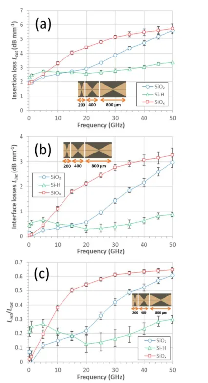
Figure 6. The insertion and interface losses in large-gap CPW. (a) The total insertion losses 𝐿𝑡𝑜𝑡 (dB mm
-1), (b) the interface losses 𝐿
𝑖𝑛𝑡 (dB mm-1), and (c) the ratio of the interface losses to total losses (𝐿𝑖𝑛𝑡⁄𝐿𝑡𝑜𝑡). Results are given for: a silicon dioxide layer present between the CPW tracks (open blue
20
circles—SiO2), a hydrogen-terminated (100) silicon surface between the CPW tracks (open green
triangles—Si-H), and a native oxide grown on the Si-H surface between the CPW tracks (open red squares—SiOx). The CPW have a length L of 1.4 mm, a signal line width 𝑠 equal to 100 µm, and a
signal-to-ground gap width 𝑔 equal to 63.5 µm.
Figure 6 shows the insertion and interface losses in the large-gap CPW. Fig. 6(a) shows the insertion losses (dB mm-1) from 0.25 GHz to 50 GHz for three different intertrack surface configurations.
First, the insertion losses (per unit length) are comparable with similar CPW in the literature. It can be observed that the HF treatment leads to a reduction of the insertion losses by approximately 0.1 dB mm-1
over the whole measurement range (green triangles). After 3 months of native oxide growth between the tracks, a very slight change in the losses is observed. Fig 5(b) shows the extracted interface losses in the large-gap CPW—these have been obtained by removing the modelled conductor and dielectric losses. Fig. 5(c) shows a plot of the ratio of the interface losses to the total insertion losses. It is seen that the ratio is approximately similar for the three intertrack surface configurations—apart from at lower frequencies, where the interface loss contribution is higher with the presence of the silicon dioxide between the tracks.
21
Figure 7. The insertion and interface losses in small-gap CPW. (a) The total insertion losses 𝐿𝑡𝑜𝑡 (dB mm
-1), (b) the interface losses 𝐿
𝑖𝑛𝑡 (dB mm-1), and (c) the ratio of the interface losses to total losses (𝐿𝑖𝑛𝑡⁄𝐿𝑡𝑜𝑡). Results are given for: a silicon dioxide layer present between the CPW tracks (open blue circles—SiO2), a hydrogen-terminated (100) silicon surface between the CPW tracks (open green
22
triangles—Si-H), and a native oxide grown on the Si-H surface between the CPW tracks (open red squares—SiOx). The small-gap CPW have a signal line width 𝑠 equal to 2 µm, and a signal-to-ground gap
width 𝑔 equal to 2.5 µm.
Figure 7 shows the result of the extraction of the insertion losses and the interface losses in the small-gap CPW. Fig. 7(a) shows the extracted insertion losses (dB mm-1) of uniquely the small-gap CPW from 0.25
GHz to 50 GHz for three different intertrack surface configurations. Overall, the insertion losses are higher than for the large-gap CPW—this has been previously seen [37]. It can be observed that the HF treatment again leads to a reduction of the insertion losses—but this time by approximately 2.5 dB mm-1 at
50 GHz (green triangles). After 3 months of native oxide growth between the tracks, a relatively large increase in the losses is observed—the losses due to the presence of the native oxide being larger than for the silicon dioxide when the measurement frequency is >10 GHz. Fig 7(b) shows the extracted interface losses in the small-gap CPW—these have been obtained using the methods described above in Section 5.1. Fig. 7(c) shows a plot of the ratio of the interface losses to the total insertion losses for the small-gap CPW. In stark contrast to the large-gap CPW—c.f. Fig. 6(c)—the contributions of the interfaces losses for the small-gap CPW depend strongly on the intertrack surface configuration. They are noticeably much lower for the intertrack hydrogen-terminated silicon surface (green triangles) compared to the two oxides (silicon dioxide and native oxide). The interface loss contribution is also higher for the native oxide (red squares) than the silicon dioxide (blue circles) in the small-gap CPW. In order to obtain Fig. 7(a), which is based on the measurement of 3 lengths of small-gap CPW, it should be noted that at all frequencies and surface conditions, when the total losses are plotted as a function of small-gap CPW length (as described in Section 5.1), the data is linear with a coefficient of determination (𝑅2) equal to near unity enabling an accurate extraction of the intercept losses at 𝑙 = 0, as described above..
23
Let us now consider and compare the contributions of the intertrack surface losses in the different intertrack surface configurations for the large-gap and the small-gap CPW.
5.4. Intertrack surface losses in large-gap and small-gap CPW
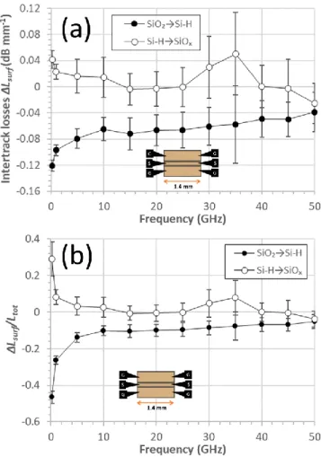
Figure 8. The intertrack surface losses in large-gap CPW. (a) The change in losses due to intertrack surface losses ∆𝐿𝑠𝑢𝑟𝑓 (dB mm-1) and (b) the ratio of the change of intertrack surface losses to the total losses (∆𝐿𝑠𝑢𝑟𝑓⁄𝐿𝑡𝑜𝑡). Results are given for the change between a silicon dioxide and a hydrogen-terminated silicon surface between the CPW tracks (SiO2→Si-H: filled circles), and the change from a
24
hydrogen-terminated silicon surface to a native oxide between the CPW tracks (Si-H→SiOx: open circles).
The CPW have a length L of 1.4 mm, a signal line width 𝑠 equal to 100 µm, and a signal-to-ground gap width 𝑔 equal to 63.5 µm.
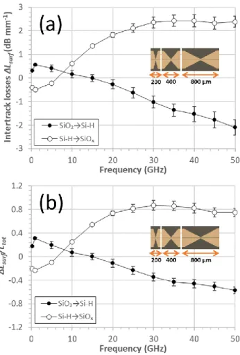
Figure 9. The intertrack surface losses in small-gap CPW. (a) The change in losses due to intertrack surface losses ∆𝐿𝑠𝑢𝑟𝑓 (dB mm-1) and (b) the ratio of the change of intertrack surface losses to the total losses (∆𝐿𝑠𝑢𝑟𝑓⁄𝐿𝑡𝑜𝑡). Results are given for the change between a silicon dioxide and a hydrogen-terminated silicon surface between the CPW tracks (SiO2→Si-H: filled circles), and the change from a
25
The small-gap CPW have a signal line width 𝑠 equal to 2 µm, and a signal-to-ground gap width 𝑔 equal to 2.5 µm.
The intertrack surface losses (∆𝐿𝑠𝑢𝑟𝑓) and their proportional contribution compared to the total losses (∆𝐿𝑠𝑢𝑟𝑓/𝐿𝑡𝑜𝑡) are shown in and for the large-gap CPW (Figure 8) and small-gap CPW (Figure 9). If we first compare Fig. 8(a) to Fig. 9(a), the data being ratios, it is apparent that the intertrack surface losses play a more important role for small-gap CPW than for large-gap CPW. In the case of the small-gap CPW—Fig. 9(a)—the change of intertrack surface configuration from silicon dioxide to hydrogen-terminated silicon (filled circles) and from hydrogen-hydrogen-terminated silicon to native oxide (open circles) leads to large changes in the losses. Fig. 8(b) and Fig. 9(b) plot these changes as a ratio of the total losses. Again, this proportion is larger for the small-gap CPW. We are now able to quantitively compare the contributions of the intertrack surface losses of the two types of CPW if we plot the ratios of these results—this is shown in Figure 10.
26
Figure 10. Comparison of the intertrack surface losses in large-gap and small-gap CPW. (a) The ratio 𝑅𝑖𝑛𝑡 corresponds to (𝐿𝑠𝑖𝑛𝑡 𝐿 𝑡𝑜𝑡 𝑠 ⁄ ) (𝐿𝑙𝑖𝑛𝑡 𝐿 𝑡𝑜𝑡 𝑙 ⁄ )
⁄ . (b) The ratio 𝑅𝑠𝑢𝑟𝑓 corresponds to
(𝛥𝐿𝑠𝑠𝑢𝑟𝑓⁄𝐿𝑠𝑡𝑜𝑡) (∆ 𝐿⁄ 𝑠𝑢𝑟𝑓𝑙 ⁄𝐿𝑙𝑡𝑜𝑡)—where the superscripts refer to small-gap (𝑠) and large-gap (𝑙). For (a) the open blue circles correspond to a 50 nm thick silicon dioxide (SiO2) present between the tracks, the
open green triangles correspond to a hydrogen-terminated silicon surface (Si-H) between the CPW tracks, and the open red squares correspond to a native oxide (SiOx) between the tracks. For (b), the filled circles
correspond to the change between a silicon dioxide and a hydrogen-terminated (100) silicon surface between the CPW tracks (SiO2→Si-H), and the filled circles correspond to the change from a
27
Figure 10 shows the comparison of the intertrack surface losses in the large-gap and small-gap CPW. The plots in Fig. 10(a) enable us to compare the contributions of the interface losses in the two types of CPW using the ratio 𝑅𝑖𝑛𝑡. The contribution of all interface losses (beneath and between the CPW tracks) is smaller for small-gap CPW in all intertrack surface configurations—except for the native oxide surface above 40 GHz where their contributions are approximately the same in the two sizes of CPW. The plots in Fig. 10(b) plot the ratio 𝑅𝑠𝑢𝑟𝑓 which directly compares the contribution of the surface losses in small-gap and large-gap CPW. For example, at 50 GHz, the contribution of the surface losses is an order of magnitude larger in the small-gap CPW than the large-gap CPW—when changing the CPW intertrack surface from silicon dioxide to a terminated silicon (filled circles) and from hydrogen-terminated silicon to a 3-month-old native oxide (open circles). Let us now discuss the physical mechanisms involved and consider reasons why this should be so.
6. Discussions
6.1. Comparisons of results with measurements on comparable CPW
Pfeifer et al [38] measured losses in Cr/Au CPW (𝑠 = 20 µm) on silicon wafers with and without a 200 nm thick silicon dioxide layer. They concluded that the inclusion of the silicon dioxide layer increases losses due to charge accumulation and inversion at the silicon dioxide/silicon dioxide interface caused by fixed oxide charges. However, they did not remove the silicon dioxide selectively from between the tracks. Ponchak [37] studied losses in CPW on high-resistivity silicon as a function of metallization dimensions, observing that a smaller signal width significantly increases losses.
Wu at al [39,40] and Gamble et al [41] conducted studies on the intertrack surface losses in CPW on silicon wafers. Wu et al [39] incorporated a silicon dioxide into CPW to reduce intertrack surface losses. Wu et al [40] and Gamble et al [41] studied losses and considered their mechanisms in large-gap CPW patterned on silicon. They showed that at 30 GHz and for CPW (𝑤 =40 µm 𝑠 = 70 µm) losses
28
decrease from ~1.8 dB mm-1 to 0.3 dB mm-1 when a 100 nm thick LPCVD oxide is selectively removed in
the CPW gap. Based on ideas proposed by Reyes et al [42], they suggested that the fixed charge in the oxide cause electrons to be attracted to the Si/SiO2 interface which forms an inversion layer between the
signal and ground tracks of the CPW—the presence of these carriers would result in increased losses due free carrier absorption near the surface. They also suggested that selective removal of the silicon dioxide—using HF—uniquely between the metallized CPW tracks removes the fixed positive oxide charges and thus the minority carrier inversion layer between the CPW tracks explaining their observed lower losses. Schollhorn et al [14] studied loss mechanisms in micropatterned CPW on oxidized (200 nm) silicon (ρ > 1000 Ω cm). They studied 50 Ω CPW having signal track widths 𝑠 equal to 20 µm and 45 µm using 1 µm thick aluminium tracks. First, they observed larger attenuation on CPW having smaller signal track width. Second, they observed lower substrate losses for higher resistivity silicon substrates. They identified bias-depended interface losses at the oxide/silicon interface under the metallisation. These losses were higher for inversion layers than accumulation layers in p-type silicon—hypothesized to be due to the larger electron mobility in silicon. The nature of the metallization meant that they were not able to remove the oxide between the tracks using HF-based wet etch solutions. Lederer and Raskin [43] considered the contributions of loss mechanisms in CPW and microstrip (MS) transmission lines on oxidized silicon. They found that CPW on a thermal oxide (SiO2) on high-resistivity (>5000 Ω cm) silicon
was more sensitive to DC biasing and its polarity than MS—implying that buried interface charges (and their absorption) underneath tracks were at the origin of a significant proportion of the losses in this system. Yuhang et al [44] proposed lower-loss a ‘V-groove’ CPW based on SOI wafers. Using CPW having a signal-to-ground gap width of 30 µm. They demonstrated lower insertion losses by removing— using selective etching—the CVD oxide and part of the silicon device layer underneath the metal tracks. They observe that the insertion losses can be reduced from >2 dB mm-1 to ~1 dB mm-1. The findings here
suggest that the reduced losses observed by Yuhang et al [44] have, at least in part, their origin at interfaces between the tracks. Finally, in terms of losses associated with a buried layer, Neve et al [45]
29
showed that a buried trap-rich layer could reduce losses of CPW on silicon having a resistivity in the range 2-5 kΩ cm.
6.2. The different CPW intertrack surfaces
It has long been known that energy band bending at the surface of a semiconductor [46] (due to deposition of materials and surface treatments) causes a modification of free carriers (electrons or holes) in proximity to the surface compared to the bulk. In CPW on semiconductors, such carriers can contribute to losses via free carrier absorption. To understand the origin of the losses in the three different intertrack surface configurations here, we need to look at these surfaces and their properties.
6.2.1. Silicon dioxide/ silicon
If an oxide is thermally- grown or deposited onto the surface of weakly-doped crystalline silicon, it is known that fixed oxide charges [47,48] can lead to the formation of a ‘natural’ inversion layer in the silicon near to the silicon-oxide interface [49]. If the silicon has a light p-type background, as is the case here, then the fixed oxide charges—which are known to be positive—will result in an inversion layer of electrons near the silicon dioxide-silicon interface. For LPCVD oxides, Ang et al [50] showed that the oxide fixed charge density is in the mid-1011 cm-2. Buchanan et al [51] observed trapped positive charge
as high as ~1012 cm-2 in CVD-grown silicon dioxide films on silicon. Using p-type (100) silicon, Gaind
and Kasprzak [52] measured a distributed oxide charge of 1.5×1015 cm-3 and an interface charge of
1.1×1010 cm-2 for a CVD oxide. Lee et al [53] showed that the interface state density of CVD oxides is in
the low-1011 cm-2 eV-1 following high-temperature annealing. The mobility of carriers in these inversion
layers has been studied by Sun and Plummer [54]. They showed that the mobility of the carriers in the inversion layer depends on the background doping of the silicon and the oxide charge density.
30
Let us consider the hydrogen-terminated (100) silicon surface resulting from a hydrofluoric acid-based treatment [55]—often used for temporary surface passivation [56] via the formation of a nonpolar Si-H bond. In terms of the stability of the hydrogen termination, following exposure to the HF-based solution, the (100) silicon surface between the metal tracks becomes hydrogen-terminated with a high surface coverage [30] and high degree of stability [31]. Using Auger electron spectroscopy, Kluth and Maboudian [57] observed a stable Si-H surface up to >100 hours after NH4F treatment of a (100) silicon surface. In
terms of the electrical properties of the Si-H surface, Weinberger et al [58] and Yablonovitch et al [59] have demonstrated the passivation of electrical sites on the surface of silicon to <1010 cm-2 using
fluorination by a number of techniques, including exposure to HF. Using surface photovoltage measurements, Angermann [60] showed that the surface Fermi level position was near zero for p-type silicon treated with an NH4F-based solution. Using moderately doped (p-type and n-type) silicon Huang
and Lau [61,62] observed that and dilute HF (<5%) treatment of silicon surface could achieve near-flatband surfaces—although others have observed Fermi-level pinning in HF-treated silicon surfaces [63,64]. Recently, using thin silicon layers, Peng et al [65] found that hydrogen-termination results in surface ‘donar-like’ states in the 1011 cm-2 eV-1 range.
6.2.3. Native oxide on a hydrogen-terminated surface
Let us consider the native oxide formed on a hydrogen-terminated silicon surface. When a hydrogenated silicon surface—obtained using an HF-based solution [55]—is exposed to oxygen in the air at room temperature, a thin native oxide slowly grows on the surface. Raider et al [32] showed that it takes 5 weeks to grow a native oxide having a thickness of 1.8 nm in air at room temperature following an HF ‘etch’—indeed, they observed a much more rapid oxidation on cleaved silicon surfaces. According to Morita et al [66], the native oxide thickness on moderately doped (100) silicon wafers, which had been treated with an aqueous HF solution before exposure to humid air (23.7°C/RH=42%) [66], varies from ~0.2 nm to ~0.8 nm over a period of ~2 to 3 months. Graf et al [67] studied native oxide growth on
HF-31
treated p-type (100) silicon wafers. They report a 0.8 nm thick SiO2 layer having formed after 6 months
exposure of the silicon surface to air. They reported very little native oxide growth (<0.1 nm) in the first day after HF treatment and exposure to air. In terms of the composition of a native oxide allowed to grow on a silicon surface at room temperature for several months following an HF treatment, Philipe and Taft [68] showed that the oxide contains no SiO2, but is composed of SiOx (1 ≤ 𝑥 < 2). Renaud et al [69] later
showed that the interface phase between this native oxide and silicon is highly disordered.
In terms of electrical properties, Shimizu and Munakata [70] showed that the surface photovoltage varies considerable for lower doped silicon during oxide regrowth. They attributed this to the influence of the fixed oxide charges on the surface depletion. Angermann et al [71] showed that the surface state distribution 𝐷𝑖𝑡 of p-type silicon (270 Ω nm and <111>) increases from 4×10¹¹ eV-1 cm-2 to 2.45×10¹² eV
-1 cm-2 over a period of 16 days of native oxide regrowth following an HF treatment—following a 𝐷
𝑖𝑡 = 6.52 × 10¹¹𝑡0.226 relationship if 𝑡 is in hours. Mizsei [72] measured the surface potential of ultra-thin silicon dioxide layers—finding a correlation between the electrical properties of the surface and the growth properties. Mizsei [73] has also shown that the bulk doping density of the silicon determines the if the free carriers at the silicon/native oxide interface are in accumulation, depletion, or inversion—for p-type silicon, the surface is in inversion.
6.3. Losses due to free carrier absorption in silicon
The absorption coefficient of free carriers in a semiconductor can be modelled based on the Drude model of conduction [74] and has proved to be a reasonable approximation [75,76]. The real and imaginary parts of the complex permittivity 𝜀 = 𝜀′− 𝑗𝜀′′ are given by:
𝜀′= 𝜀 𝑆𝑖(1 − 𝜔𝑝2𝜏2 1+𝜔2𝜏2) (9) 𝜀′′= 𝜀 𝑆𝑖 𝜔𝑝2𝜏 𝜔(1+𝜔2𝜏2) (10)
32
Where 𝜔 is the angular frequency (𝜔 = 2𝜋𝑓), 𝜀𝑆𝑖 is the dielectric constant of silicon, 𝜏 is the average scattering time, and 𝜔𝑝 is the plasma frequency which is given by:
𝜔𝑝= √ 𝑛𝑞2 𝑚∗𝜀
𝑆𝑖 (11)
where 𝑛 is the carrier density, 𝑞 is the elementary charge, and 𝑚∗ is the effective mass of the carriers. The average scattering time 𝜏 is given by:
𝜏 =𝑚∗
𝑞 𝜇 (12)
where 𝜇 is the mobility of the charge carriers.
The dielectric constant of silicon 𝜀𝑆𝑖, the elementary charge 𝑞, the mass of the electron 𝑚𝑒, the vacuum permittivity 𝜀0, and the speed of light are taken to be: 11.9, 1.6×10¹⁹ C, 9.11×10⁻³¹ kg, 8.85×10⁻¹² Fm-1, and 3×10⁸ ms-1, respectively. The following values of carrier mobility and effective mass are used
for lightly doped silicon: (electrons: 1500 cm2 V-1 s-1 and 0.26𝑚
𝑒) and (holes: 450 cm2 V-1 s-1 and 0.37𝑚𝑒). The effective masses are those used in conductivity calculations--although it should be noted that the mobilities in surface inversion layers are modified [54].
Finally, the absorption coefficient 𝛼 (per unit length) is given by:
𝛼 =𝜔 𝑐𝐼𝑚√𝜀
′− 𝑗𝜀′′ (13)
Where 𝐼𝑚√𝜀′− 𝑗𝜀′′ is the imaginary part of the square root of the complex permittivity.
Figure 11 shows plots of the calculated absorption coefficient 𝛼 of free carriers (Fig. 11(a) – electrons and Fig. 11(b) – holes) in silicon as a function of frequency and free carrier density.
33
Figure 11. Plots of the calculated absorption coefficient 𝛼 versus frequency for different values of carrier density 𝑛/𝑝 of (a) electrons and (b) holes. The dashed light blue line in (a) shows the absorption coefficient for a maximum electron density (4.5×1013 cm-3) generated by background lighting. The dashed
light blue line in (b) shows the absorption coefficient for the maximum hole background density (1.46×1013 cm-3) of the bulk silicon-on-insulator wafers used for the study.
There are several observations which can be made from Fig. 11 in the context of losses in CPW. First, for both carriers (electrons and holes), the absorption coefficient increases with frequency. Second, the absorption coefficient is larger for electrons than holes at all frequencies—this should be apparent in CPW on semiconductor surfaces which favour either electron or hole accumulation, depletion, or
34
inversion. Third, for both types of carriers, at higher frequency, the change in absorption coefficient is more sensitive to a change in free carrier density, i.e. at higher frequency, the losses associated with free carrier absorption in CPW will be sensitive to changes in the free carrier density where the electric field energy is high, i.e. between the tracks. Finally, the sensitivity of the absorption coefficient to variations in the carrier density suggests that gains are to be made in terms of losses by reducing free carrier presence where electric field energy density is high.
We are now in a position to tentatively link the experimentally-observed changes in the attenuation coefficient of the line ∆𝛼𝑑𝐵 (assumed to be due to a change in free carrier absorption) with the computed changes in the absorption coefficient of silicon due to excess free carriers ∆𝑛, i.e. ∆𝛼𝑑𝐵∝ ∆𝛼𝑁𝑝≅ ∆𝛼 = 𝑓(∆𝑛). Let us consider the experimental results obtained using the small-gap CPW. With reference to Fig. 9(a), the change in surface losses at 50 GHz is ~2 dB mm-1 when hydrogenating or
oxidizing the intertrack silicon surface. This is equivalent to a change in the absorption coefficient 𝛼 of ~23 cm-1. It can be seen from Fig. 11(a) that at 50 GHz this would correspond to an approximate change
of ~2×1015 cm-3 free carriers—an electron inversion layer [54,77]—near the surface. When multiplied by
the Debye length, this results in a surface charge equal to ~2.3×1011 cm-2—a value which agree well with
the value calculated analytically by Deal et al [49]. This values is also comparable with that given by Wu
et al [39] and Gamble et al [41]. The free-carrier loss modelling and our experimental observation a
suggest that the free-charge density near the hydrogen-terminated silicon surface between the tracks is of the order of the background doping density of the silicon ~1.5×1013 cm-3. We can now understand the
schematic representation of the charges given in Fig. 2. Using the empirical relationship given in Sun and Plummer [54], the effective electron mobility in the inversion layer is calculated to be ~1000 cm2 V-1 s-1
for 𝑁𝐴 = 1.47×1013 cm-3 and a surface charge equal to 2.3×1011 cm-2—this does not significantly change the absorption coefficient.
35
Finally, as most microwave measurements are performed in a lit room, we will consider and compute the effect of a low background irradiance on the carrier concentration at the surface of the silicon between the tracks. This irradiance of our weak background lighting is calculated to be 60 µW cm-2. This
level of irradiance leads to a small excess carrier concentration which depends on the surface of the silicon—due to the change in surface recombination velocity. For hydrogen-terminated silicon the average excess carrier concentration within a Debye length (~1 µm – see Supplementary Information) is 4.4×10¹³
cm-3, for a native oxide ‘grown’ on an initially hydrogen-terminated silicon surface for several months in
air at room temperature, the average excess carrier concentration within a Debye length is 3×1012 cm-3—
see Supplementary Information for details of the calculation. It should be noted that higher irradiance incident light can modify losses in CPW (see Supplementary Information) but study have found that irradiances in the range 0.2-3 W cm-2 do not alter the observed losses [78,79].
6.4. Estimation of the contribution of intertrack surface losses
There are examples in the literature of attempts to characterize and model the contribution of the intertrack surface losses. Barends et al [80] pointed out the importance of surface losses on a ‘bare’ silicon substrate. They showed that these losses increase by a factor of ~8 when reducing the CPW signal track width from 100 µm to 1 µm. They proposed and demonstrated the technological solution of etching the silicon away between the tracks where the electric field is highest. Wenner et al [17] were surprised to find the substrate-air losses contribute considerably to total losses in CPW compared with microstrip. They computed the ‘substrate-air’ losses to be ~3 times larger for small gap (2 µm) CPW compared to large-gap (20 µm) CPW. The role of amorphous and native oxides on intertrack surface losses in superconducting CPW resonators has been pointed out [81,82] which has led to work concerning the modelling of interface losses. Murray et al [83] developed an analytical model based on electrostatics to compute the contribution (termed participation 𝑃) of ‘surface-air’ losses to the total losses 𝑃𝑠𝑎. To do this they
36
computed the ratio of the electric field energy, residing in a small volume having thickness 𝛿 at the substrate surface between the tracks of planar electrodes 𝑈𝑠𝑎 to the total electric field density 𝑈𝑡𝑜𝑡. Figure 12 shows a schematic diagram of the electric field lines tin the case of two CPW having different gap sizes. The important point is that the intertrack losses are associated with the proportion of the total energy of the electric field near to the surface (red circles)—this energy ratio is not the same as the gap size is shrunk.
Figure 12. Schematic diagram showing electric field lines associated with (a) ideal large-gap and (b) small-gap CPW. The red circles indicated the proportion of the total electric field energy residing in a small volume of space between the CPW tracks. This energy proportion is not the same as the gap distances are diminished. Smaller CPW have a higher proportion of electric field energy (compared to the total electric field energy) between the gaps than large-gap CPW.
37 𝑃𝑠𝑎( 𝛿 𝑎) ≈ 𝜀𝑐 (𝜀𝑠𝑢𝑏+1) 1 2(1−𝑘)𝐾(𝑘′)𝐾(𝑘)( 𝛿 𝑎) {ln [4 ( 1−𝑘 1+𝑘)] − 𝑘 ln(𝑘) (1+𝑘) + 1 − ln ( 𝛿 𝛼)} (14)
Where 𝑘 = 𝑎 𝑏⁄ , 𝑘′= √1 − (𝑎 𝑏⁄ )2, 𝐾(𝑘) and 𝐾(𝑘′) are the elliptic integrals of 𝑘 and 𝑘′, 𝜀
𝑐 and 𝜀𝑠𝑢𝑏 are the relative permittivities of the surface layer and the substrate and a and b can be equated to the dimensions of a CPW to be: 𝑤 = 2𝑎 and 𝑠 = 𝑏 − 𝑎. Their calculations agree well with a numerical FEM analysis [17]. This model predicts that there are proportionally higher losses associated with the surface as the dimensions of CPW shrink.
By using the coplanar dimensions in the experimental work here, the contribution of the intertrack surface losses in CPW can be computed. Figure 13 shows a calculation of the participation of the surface-air losses 𝑃𝑠𝑎 as a fraction of the total losses in coplanar waveguide based on the above equation. The computed loss participation is given as a function of surface depth 𝛿 as explained above. The CPW dimensions used for the calculation correspond to the large-gap CPW (filled black circles) and small-gap CPW (open black circles) used to obtain the experimental results. The ratio of the loss participations 𝑃𝑠𝑎𝑠𝑚𝑎𝑙𝑙⁄𝑃𝑠𝑎𝑙𝑎𝑟𝑔𝑒 is shown by open diamonds. The model predicts that the surface-air loss participation is larger for the small-gap CPW. In the case if we consider a surface depth range of 0.1-1 µm, the model also approximately predicts the ratio of the surface losses 𝑅𝑠𝑢𝑟𝑓 observed experimentally above 20 GHz—see
c.f. Fig. 10(b). Incidentally, the Debye length of the silicon at this doping density is ~1 µm—see the
38
Figure 13. Calculation of the participation of the surface-air losses 𝑃𝑠𝑎 as a fraction of the total losses in coplanar waveguide. The loss participation is given as a function of surface depth 𝛿. The CPW dimensions used for the calculation correspond to the large-gap CPW (filled black circles) and small-gap CPW (open black circles) used to obtain the experimental results. The ratio of the loss participations 𝑃𝑠𝑎𝑠𝑚𝑎𝑙𝑙⁄𝑃𝑠𝑎𝑙𝑎𝑟𝑔𝑒 is shown by open diamonds. The values of 𝜀𝑐 and 𝜀𝑠𝑢𝑏 are 5 and 11.7. The values of the elliptic integrals 𝐾(𝑘) and 𝐾(𝑘′) were evaluated numerically to be 1.59 and 2.84 for the large-gap CPW and 1.63 and 2.4 for the small-gap CPW. The lines linking the data points are not analytical function fits.
7. Conclusions
In the case of large-gap CPW (signal track width 𝑠 = 100 µm and track spacing 𝑔 = 63.5 µm) patterned on silicon-on-insulator (SOI) wafers, selective removal of the silicon dioxide from between the CPW tracks (using buffered HF) results in some reduced losses—e.g. from 0.79 dB mm-1 to 0.69 dB mm-1 at 50 GHz.
Subsequently, a native oxide growth on the hydrogen-terminated (100) silicon surface between the CPW tracks results in no significant change in losses. In the case of small-gap CPW (𝑠 = 2 µm, 𝑔 = 2.5 µm) of patterned onto SOI, selective removal of the silicon dioxide from between tracks reduces losses
39
considerably—e.g. from 5.6 dB mm-1 to 3.4 dB mm-1 at 50 GHz. However, native oxide regrowth over a
period of months on the silicon surface between the CPW tracks leads to a significant increase in losses to 5.8 dB mm-1 at 50 GHz. The removal of this native oxide using an HF-based solution, even after years of
growth, demonstrates that the losses revert to their low value observed after removal of the thin film silicon dioxide—this proves the role of the oxide (thin film or native) in the loss mechanism. We suggest that technologies employing miniature CPW on silicon should take intertrack surface losses into account. The native oxide should be routinely removed if possible, or fabrication processes should incorporate stable surface passivation of the silicon surface specifically between the CPW tracks to avoid native oxide growth following manufacture. Finally, the observed sensitivity of the miniature CPW characteristics to the intertrack surface state suggests that miniaturization could be beneficial for sensitivity enhancement in CPW-based biosensing applications [7,84].
Acknowledgements
The authors would like to thank to thank the following people for their invaluable technical input: F. Vaurette for help with the electron beam lithography, A. Fattorini for help with the metallization, and D. Desremes for help with the AFM measurements. This work was financially supported by a French ‘Equipex’ project ‘Excelsior’ and partially supported by the French Renatech network. The digital microscope was purchased within the ‘TIPTOP_1’ project (ANR-16-CE09-0029).
ORCID iDs
40
References
[1] Wen C P 1969 Coplanar Waveguide: A Surface Strip Transmission Line Suitable for Nonreciprocal Gyromagnetic Device Applications IEEE Trans. Microw. Theory Tech. 17 1087–90
[2] Simons R N 2001 Coplanar Waveguide Circuits, Components, and Systems (New York: John Wiley & Sons, Inc.)
[3] Rogers J W M and Plett C 2010 Radio frequency integrated circuit design (Boston: Artech House) [4] Kandala A, Mezzacapo A, Temme K, Takita M, Brink M, Chow J M and Gambetta J M 2017
Hardware-efficient variational quantum eigensolver for small molecules and quantum magnets
Nature 549 242–6
[5] Göppl M, Fragner A, Baur M, Bianchetti R, Filipp S, Fink J M, Leek P J, Puebla G, Steffen L and Wallraff A 2008 Coplanar waveguide resonators for circuit quantum electrodynamics J. Appl. Phys. 104 113904
[6] Marzouk J, Arscott S, Fellahi A E, Haddadi K, Lasri T, Christophe Boyaval and Dambrine G 2015 MEMS probes for on-wafer RF microwave characterization of future microelectronics: design, fabrication and characterization J. Micromechanics Microengineering 25 075024
[7] Mehrotra P, Chatterjee B and Sen S 2019 EM-Wave Biosensors: A Review of RF, Microwave, mm-Wave and Optical Sensing Sensors 19 1013
[8] Chen Y-F, Wu H-W, Hong Y-H and Lee H-Y 2014 40 GHz RF biosensor based on microwave coplanar waveguide transmission line for cancer cells (HepG2) dielectric characterization Biosens.
Bioelectron. 61 417–21
[9] Wiemann Y, Simmendinger J, Clauss C, Bogani L, Bothner D, Koelle D, Kleiner R, Dressel M and Scheffler M 2015 Observing electron spin resonance between 0.1 and 67 GHz at temperatures between 50 mK and 300 K using broadband metallic coplanar waveguides Appl. Phys. Lett. 106 193505
[10] Mederos-Henry F, Hermans S and Huynen I 2017 Coplanar waveguide method for microwave and ferromagnetic resonance characterization of nanocarbon powders decorated with magnetic nanoparticles Microw. Opt. Technol. Lett. 59 2330–5
[11] Daffe K, Marzouk J, Fellahi A E, Xu T, Boyaval C, Eliet S, Grandidier B, Arscott S, Dambrine G and Haddadi K 2017 Nano-probing station incorporating MEMS probes for 1D device RF on-wafer characterization 2017 47th European Microwave Conference (EuMC) 2017 47th European Microwave Conference (EuMC) (Nuremberg: IEEE) pp 831–4
[12] Merla C, Liberti M, Marracino P, Muscat A, Azan A, Apollonio F and Mir L M 2018 A wide-band bio-chip for real-time optical detection of bioelectromagnetic interactions with cells Sci. Rep. 8 5044 [13] Gopinath A 1982 Losses in Coplanar Waveguides IEEE Trans. Microw. Theory Tech. 30 1101–4
41
[14] Schollhorn C, Weiwei Zhao, Morschbach M and Kasper E 2003 Attenuation mechanisms of aluminum millimeter-wave coplanar waveguides on silicon IEEE Trans. Electron Devices 50 740–6 [15] Sage J M, Bolkhovsky V, Oliver W D, Turek B and Welander P B 2011 Study of loss in
superconducting coplanar waveguide resonators J. Appl. Phys. 109 063915
[16] Woods W, Calusine G, Melville A, Sevi A, Golden E, Kim D K, Rosenberg D, Yoder J L and Oliver W D 2019 Determining Interface Dielectric Losses in Superconducting Coplanar-Waveguide Resonators
Phys. Rev. Appl. 12 014012
[17] Wenner J, Barends R, Bialczak R C, Chen Y, Kelly J, Lucero E, Mariantoni M, Megrant A, O’Malley P J J, Sank D, Vainsencher A, Wang H, White T C, Yin Y, Zhao J, Cleland A N and Martinis J M 2011 Surface loss simulations of superconducting coplanar waveguide resonators Appl. Phys. Lett. 99 113513
[18] Calusine G, Melville A, Woods W, Das R, Stull C, Bolkhovsky V, Braje D, Hover D, Kim D K, Miloshi X, Rosenberg D, Sevi A, Yoder J L, Dauler E and Oliver W D 2018 Analysis and mitigation of interface losses in trenched superconducting coplanar waveguide resonators Appl. Phys. Lett. 112 062601 [19] Wisbey D S, Gao J, Vissers M R, da Silva F C S, Kline J S, Vale L and Pappas D P 2010 Effect of
metal/substrate interfaces on radio-frequency loss in superconducting coplanar waveguides J.
Appl. Phys. 108 093918
[20] Quintana C M, Megrant A, Chen Z, Dunsworth A, Chiaro B, Barends R, Campbell B, Chen Y, Hoi I-C, Jeffrey E, Kelly J, Mutus J Y, O’Malley P J J, Neill C, Roushan P, Sank D, Vainsencher A, Wenner J, White T C, Cleland A N and Martinis J M 2014 Characterization and reduction of microfabrication-induced decoherence in superconducting quantum circuits Appl. Phys. Lett. 105 062601
[21] Bruno A, de Lange G, Asaad S, van der Enden K L, Langford N K and DiCarlo L 2015 Reducing intrinsic loss in superconducting resonators by surface treatment and deep etching of silicon substrates Appl. Phys. Lett. 106 182601
[22] Clarke J S, Thomas N, Roberts J, Pilliarisetty R, Yoscovits Z, Caudillo R, George H, Singh K J, Michalak D, Amin P, Mei A, Bruno A, Poletto S, Boter J, Droulers G, Kalhor N, Samkharadze N, Dehollain J P, Yeoh L, Sammak A, Scappucci G, Veldhorst M, DiCarlo L and Vandersypen L M K 2016 Quantum computing within the framework of advanced semiconductor manufacturing 2016 IEEE
International Electron Devices Meeting (IEDM) 2016 IEEE International Electron Devices Meeting
(IEDM) (San Francisco, CA, USA: IEEE) p 13.1.1-13.1.3
[23] Krantz P, Kjaergaard M, Yan F, Orlando T P, Gustavsson S and Oliver W D 2019 A quantum engineer’s guide to superconducting qubits Appl. Phys. Rev. 6 021318
[24] Morello A, Tosi G, Mohiyaddin F A, Schmitt V, Mourik V, Botzem T, Laucht A, Pla J J, Tenberg S, Savytskyy R, Madzik M, Hudson F, Dzurak A S, Itoh K M, Jakob A M, Johnson B C, McCallum J C and Jamieson D N 2018 Scalable quantum computing with ion-implanted dopant atoms in silicon 2018
IEEE International Electron Devices Meeting (IEDM) 2018 IEEE International Electron Devices
Meeting (IEDM) (San Francisco, CA: IEEE) p 6.2.1-6.2.4


![[PDF] Formation Access les requetes et etats | Cours informatique](data:image/gif;base64,R0lGODlhAQABAIAAAP///wAAACH5BAEAAAAALAAAAAABAAEAAAICRAEAOw==)