HAL Id: hal-02815172
https://hal.archives-ouvertes.fr/hal-02815172
Preprint submitted on 6 Jun 2020
HAL is a multi-disciplinary open access
archive for the deposit and dissemination of
sci-entific research documents, whether they are
pub-lished or not. The documents may come from
teaching and research institutions in France or
abroad, or from public or private research centers.
L’archive ouverte pluridisciplinaire HAL, est
destinée au dépôt et à la diffusion de documents
scientifiques de niveau recherche, publiés ou non,
émanant des établissements d’enseignement et de
recherche français ou étrangers, des laboratoires
publics ou privés.
”Negative group delay experimentation with tee
connector and cable structures”, Eur. Phys. J. Appl.
Phys. (EPJAP)
Fayu Wan, Xiaoyu Huang, Preeti Thakur, Atul Thakur, Sébastien Lallechere,
Blaise Ravelo
To cite this version:
Fayu Wan, Xiaoyu Huang, Preeti Thakur, Atul Thakur, Sébastien Lallechere, et al.. ”Negative group
delay experimentation with tee connector and cable structures”, Eur. Phys. J. Appl. Phys. (EPJAP).
2020. �hal-02815172�
Page 1 of 20
Negative group delay experimentation with tee connector and cable structures
Fayu Wan1, Xiaoyu Huang1, Preeti Thakur2, Atul Thakur2, Sébastien Lalléchère3, and Blaise Ravelo1
1Nanjing University of Information Science & Technology, Nanjing, China 2Amity University Haryana, Gurgaon, 122413 India
3 Université Clermont Auvergne, Institut Pascal, SIGMA Clermont, 4 av Blaise Pascal, F-63178 Aubière, France
e-mail: [email protected], [email protected], [email protected], [email protected], [email protected], [email protected]
Corresponding author e-mail: [email protected]
Abstract: The unfamiliar negative group-delay (NGD) phenomenon is experimented with structure constituted by
tee-connectors and coaxial cables. The topology of the NGD generator is described. It consists of two parallel 50-Ω characteristic impedance cables. The S-parameter model in function of the cable physical lengths is established. The existence condition enabling to understand the NGD phenomenon is defined. A proof of concept simply is constituted by two three-port SMA connectors, three SMA transitions and 13-cm length cables. The NGD experimentation is performed from 1.5 GHz to 3.5 GHz. Tri-band NGD aspects in good agreement with the theory and simulation is observed experimentally. Particularly, high figure-of-merit NGD circuit with -3 ns NGD level, less than 2 dB insertion loss and 12 dB return loss around 3 GHz centre frequency is measured.
Keywords: Negative group delay (NGD), NGD analysis, NGD experimentation, Tee-cable network, S-parameter model.
Acknowledgement: This research work was supported in part by NSFC under Grant 61601233 and Grant
61750110535, in part by the Defense Research Foundation under Grant 6140209050116ZK53001, in part by NSF of Jiangsu under Grant BK20150918, in part by the Jiangsu Innovation and Enterprise Group Talents Plan 2015 under Grant SRCB201526, and in part by PAPD.
Author Contributions:
- Fayu Wan performed the main writing of the paper and was a part of NUIST, China.
- Xiaoyu Huang performed the test and the data processing and was a Master student of NUIST, China. - Preeti Thakur and Atul Thakur contributed on the technical and English correction of the paper. - Sébastien Lalléchère performed result verifications by simulation.
- Blaise Ravelo was the main initiator of the NGD cable-connector structure and the development of the NGD theory.
- All authors contributed on the article writing with critical reviews and corrections.
Page 2 of 20
1. INTRODUCTIONThe group delay (GD) may affect the transmission signal quality in the communication systems [1-6]. In addition, with the dispersion effect [1], the group delay can become non flat in the operation frequency bands of RF and microwave components. Depending on the application area, such degradation effects are interpreted with different analytical parameters group- [1-2], propagation- [3-4] and time- [5-6] delays. Therefore, an efficient technique is necessary for estimating the influence of delays on the communication quality [5-6]. In addition, effective technical solutions have been deployed to overcome the delay effects as the development of design methods dedicated to group delay equalizers [7-9], minimizer [10] and linearizer [11] were proposed. So far, different techniques to design equalizers were introduced with typically all-pass network filters [12]. Nevertheless, these types of equalizers have negative undesirable effects as the generation of additional positive group delays. The uncontrollable group delays are not good and may degrade the system performance.
An alternative technique of equalizer implementation using negative group delay (NGD) function was introduced in [13]. This type of NGD equalizer enables to realize outstanding solutions as the neutralization of undesirable RC- and LC-effects generally degrading the signals propagating through the electrical interconnections [4]. However, nowadays, in difference to the other classical functions, the NGD phenomenon is still not understandable for most of electronics, RF and microwave engineers. For this reason, the present paper investigates an experimentation of NGD phenomenon with a non-complicated electrical structure.
Since the first experimentation of NGD phenomenon in 1990s, few groups of research are currently working on this counterintuitive topic. Nevertheless, various non mature attempts of applications in particular in the area of RF and microwave engineering were proposed [13-26]. As reported in [14], an NGD compensation method of oscillators, filters and communication systems was initiated [14]. Another compensation method of array antenna effect based on the NGD circuit fabricated with lossless double negative metamaterials can be found in [15]. Design of matched bridged tee network with positive phase slope was studied in [16]. But, the passive NGD circuits used in these applicative proposals suffer from attenuation losses. To alleviate this roadblock, alternative applications with NGD active circuits were proposed [17-22]. For example, a design method of enhanced bandwidth feedforward amplifier using NGD resonator was presented in [17-18]. More recently, another design of bidirectional amplifier with NGD matching circuits was investigated in [19-21]. A design method of distributed amplifier using reconfigurable NGD circuit is presented in [22]. Different antenna design applications were also proposed as the arbitrary-angle squint-free beamforming in series-fed antenna arrays using non-Foster NGD networks [23]. Then, design method of arbitrary terminated unequal coupler with bandwidth-enhancement by using NGD circuit is proposed in [24]. Designs of NGD devices and circuits for RF and microwave front- and back-end chains based were also invented [25-26]. In spite of those applications, today, the NGD function can be classified as the most uncommon electronic function for most of researchers and engineers.
To feed our knowledge on the uncommon NGD phenomenon, a brief state-of-the-art is narrated in this paragraph. Basically, the NGD phenomenon can be identified with its outstanding signature of the apparition of output signal in advance of smoothed input [27]. Knowing the initial interpretation of the group delay [28-29], it can be understood
Page 3 of 20
that the NGD phenomenon can be generated systematically when a linear circuit transmission phase presents a positive slope when the frequency increases [28-29]. The first NGD synthesizer with typically RLC-resonator passive network was investigated in [30-31]. One decade later, NGD passive resonant circuits inspired from double negative metamaterial structures were designed [32-34]. The NGD function meaning in time-domain with the negative delay was theoretically investigated and experimented in [27]. However, it was emphasized in [35] that the NGD circuit must operate with limited time-advance. Nevertheless, last decade, some innovative circuits operate with NGD phenomenon were developed [36-46]. Non-Foster reactive elements NGD passive networks were proposed [36]. Maximally flat NGD active circuit by exploiting the transversal filter concept is proposed [37]. Then, design of passive NGD lumped circuit with modified lossy left-handed metamaterial structure is proposed in [38]. Mostly, the NGD circuits using lumped passive elements are significantly lossy. Therefore, NGD circuits with distributed transmission lines (TLs) were proposed [39-45]. Transmission type NGD distributed passive circuits were also introduced [39-41]. Another NGD distributed passive circuits based on the coupling effect were proposed in [44-45]. This tremendous progress of NGD design should be accompanied to pedagogical experimental open technique to make the topic more familiar to non-specialists.
As discussed previously, further illustrative theory and experimentation is necessary to illustrate and explain the NGD phenomenon. More research work must be performed to open the NGD topic to non-specialist including RF and microwave engineering community. Simpler NGD topology operating with lower loss and good access matching remains an open topic of research. For this reason, the present paper introduces an easy to understand NGD investigation. To do this, particularly simple structure constituted by SMA Tee-Connectors and SMA cables operating as a bandpass NGD function is presented. In difference to the previous NGD study [13-27,30-45], the present work develops an innovative theory and experimentation demonstrating the possibility to generate the NGD phenomenon in function of the SMA cable length and attenuation. Thus, the proposed structure is helpful for understanding the NGD function. It can be experimented easily with simple SMA connectors and cables by non-specialists.
The paper is organized in four main sections. Section 2 describes the theoretical investigation of the Tee-Cable topology. The proposed topology is designed with only distributed elements without lossy lumped elements. The circuit theory is elaborated from the S-parameter modelling. The NGD analyses will be introduced in Section 3. The NGD existence equations and centre frequencies in function of the cable delay and attenuation are investigated. Section 4 is focused on the practical validations including the NGD experimentation of the tee connector combined with coaxial cables. Proof-of-concept (POC) built with Tee-Cable based structure will be described. Comparisons between the analytically calculated, simulated and experimented results will be discussed. Then, the last Section presents the conclusion of the paper.
Page 4 of 20
This section is focused on the NGD theory. The equivalent circuit of the Tee-Cable structure will be introduced. The S-parameter model will be calculated. The group delay expression will be established in order to perform the NGD analysis.
2.1 Description of the Tee connector and cable structure
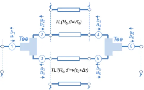
The NGD microwave circuit under study behaves as a two-port passive topology. In difference to work published in [13-27], the present NGD topology is constituted by interconnected three-port Tee connectors and cables represented by TLs. The connector terminals are referenced by the elements with connection Ports -- and Ports --. For the shake of mathematical simplicity, the constituting connectors are represented by ideal three port S-matrix. As depicted in Fig. 1, connector port and port represent respectively as the overall NGD topology main input and output.
Fig. 1. Equivalent schematic of the combined tee connectors and cables network under study.
The overall circuit is loaded by R0=50 Ω which is assumed as the reference impedance. Ports and are directly connected and ports and are interconnected through a lossy cable with characteristic impedance R0 and physical length d. The variables am and bm (m={1,…,6}) represent the input and output wave powers propagating through the
structure branches. The proposed topology S-parameter modelling will be described in the next paragraph.
2.2 Theoretical modelling of S-matrix
This analytical study is elaborated by supposing that the Tee connector with negligible physical length and the cable is perfectly matched. By hypothesis, the three-port Tee connector S-parameter model is symmetrically expressed as:
2 / 31 / 3 2 / 31 / 3 2 / 32 / 3 2 / 3 2 / 3 1 / 3 Tee S − = − − . (1)This Tee connector S-matrix can be operated with the topological parameters of the circuit based on the following the matrix relation:
Page 5 of 20
1 1 2 2 3 3 Tee b a b S a b a = , (2) and:
6 6 4 4 5 5 Tee b a b S a b a = . (3)In this paper, the interconnect lossy cable characteristic impedance is assumed equal to Zc=R0. By denoting v the wave speed, the cable physical length is expressed as:
d=v∙τ0. (4)
The lossy cable is characterized by the parameter:
a=e-αd<1, (5)
with α is the attenuation constant. Under this hypothesis, by denoting the angular frequency variable ω, the interconnect reflection and insertion losses introduced in [39-45] become:
0 11 22 12 21 ( ) ( ) 0 ( ) ( ) TL TL j TL TL S j S j S j S j a e − = = = = , (6) 0 0 11 22 ( ) ( ) 12 21 ( ) ( ) 0 ( ) ( ) TL TL j j TL TL S j S j S j S j b e a e − + − + = = = = , (7) with: τ0=d/v, (8) and Δτ=Δd/v, (9)
are the cable delay. These S-parameters are linked to the access port wave powers by the matrix relation:
2 11 21 2 4 21 11 4 TL TL TL TL a S S b a S S b = , (10) 3 11 21 3 5 21 11 5 TL TL TL TL a S S b a S S b = . (11)
Consequently, we have the power wave expressions:
0 0 2 4 4 2 j j a a e b a a e b − − = = , (12) 0 0 ( ) 3 5 ( ) 5 3 j j a b e b a b e b − + − + = = . (13)
2.3 Frequency dependent expression of S-parameter coefficients
Page 6 of 20
relation: 1 11 22 1 6 12 21 1 ( ) ( ) ( ) ( ) b S j S j a b S j S j a = = = = . (14)These coefficients can be expressed in function of the circuit parameters by calculating the output wave powers b1 and b6, and the input wave power a1. First, b1 and b6 can be determined by successive combination of the wave powers propagating through the cable and connector access ports. The analytical expressions obtained from the S-matrices defined previously in equations (1), (6) and (7) give the simplified formulas:
0 0 0 0 0 0 0 2 (2 ) 2 (2 ) 2 ( ) 4 2 2 2 11 22 2 ( ) 2 2 (2 ) 2 3 3 8 ( ) ( ) 3 j j j j j j j a e a e a e a e S j S j a e e a e − + − − + − + − − + − + + + − + = = + − − , (15) 0 0 0 0 0 (2 ) 2 12 21 2 ( ) 2 2 (2 ) 2 4 (1 ) 1 ( ) ( ) 3 j j j j j j ae e a e S j S j a e e a e − − − + − − + − + + − = = + − − . (16)
The associated reflection coefficient magnitude S11( ) =S11(j) is written as:
2 2 4 2 4 2 0 0 0 0 2 2 2 2 0 0 0 0 11 2 2 0 0 03 3 cos 2 (2 ) cos(2 ) 3 sin 2 (2 ) sin(2 )
8 cos (2 ) cos 2 ( ) 8 sin (2 ) sin 2 ( )
( ) 3 cos (2 ) cos ( ) cos( ) a a a a a a a a S a a a a + + + − + + − + + + + + + + = − + + + + +
2 2 0 0 0 2 2 2 2 0 0 0 0 0 0 sin (2 ) sin ( ) sin( ) cos (2 ) 3 sin (2 )cos ( ) cos( ) sin ( ) sin( )
a a a a a a a a + + + + + − + + + + + + + + (17)
The transmission coefficient magnitude S21( ) =S21(j) is given by:
2 2 2 2 0 4 2 0 21 2 2 2 0 0 0 2 2 0 0 1 cos (2 ) 4 1 cos( ) sin ( ) sin (2 ) ( )cos ( ) s cos( ) cos ( ) s cos
3 cos( ) 3 sin( ) sin ( ) sin( ) a a a S a a a a a a a a a − + + + + + = + + + − + − − + + −
2 0 2 2 0 0 ( ) 3 cos( ) 3 sin( ) sin ( ) sin( ) a a a a a − − − + + − , (18)With the presence of sin(.) and cos(.) terms, we can understand that these magnitudes are periodical function.
2.4 Frequency dependent expression of GD
By denoting the transmission phase associated to S21 is defined as:
21
( )=arg S (j )
Page 7 of 20
In circuit theory, the NGD phenomenon can be easily understood based on the group delay (GD) analytical definition. To do this, it is worth to recall this definition. The analytical expression of GD was initiated in [26-27]:
( ) ( )=− . (20)
The proposed cell NGD fundamental properties and characteristics will be deduced from this transmission coefficient expression. The associated transmission phase is:
( ) n( ) d( ) = − , (21) with:
2 0 0 2 0 sin (2 ) sin( ) ( ) arctan arctan 1 cos (2 ) 1 cos( ) n a a + = − − − + + , (22) and: 1 2 ( ) ( ) ( ) d d d = + , (23) where:
0 0 1 0 0 0sin( ) sin( ) sin ( )
( ) arctan
3 cos( ) cos ( ) cos (2 )
d a a a a + + + = − + + + + , (24)
0
0
2 0 0 0sin( ) sin( ) sin ( )
( ) arctan
cos (2 ) cos( ) cos ( ) 3
d a a a a + − + = + − − + − . (25)
It yields the GD defined earlier in (20) can be formulated as:
1 2 ( ) n( ) d( ) d ( ) = + + , (26) with:
2 2 0 0 0 4 2 0 (2 ) cos (2 ) ( ) 2 1 2 cos (2 ) n a a a a + − + = − + + − + , (27)
2 2 2 0 0 0 2 2 0 0 0 0 1 4 2 2 2 0 0 0 (1 )(2 ) 3(1 ) (3 ) ) cos ( )3( 1) 2 ) cos( ) (2 ) cos( ) 3cos (2 )
( )
2 9 2 cos( ) 3cos (2 ) 2 ( 3) cos( ) cos ( )
d a a a a a a a a a a a a a + + − − + − + + − + + + − + = + + + − + + − + + , (28) and:
2 2 2 0 0 0 2 2 0 0 0 0 2 4 2 2 2 0 0 0 (1 )( ) 3(1 ) (3 ) ) cos ( )3(1 ) 2 cos( ) (2 ) cos( ) 3cos (2 )
( )
2 9 2 cos( ) 3cos (2 ) 2 (3 ) cos( ) cos ( )
d a a a a a a a a a a a a a + + + + + − + + − − + + − + = + + + − + + − + + .(29)
It can be pointed out that the frequency responses (transmission and reflection coefficients, and the group delay behave as periodical functions depending to the parameters 0 and . Therefore, we are proposing to conduct the analytical analyses at some particular frequencies in the next paragraph
Page 8 of 20
3. NGD ANALYSIS AT PARTICULAR FREQUENCIESThis section develops the main physical approach on the NGD analysis.
3.1 Identification of particular frequencies
For the preliminary analytical observation, the NGD analysis can be performed at the particular values of angular frequencies. The reference angular frequency is linked to the quarter wavelength of the cable physical length:
0 0 2(2 ) = + . (30)
The analyses are performed at very low frequencies ω≈0 and the multiple of the particular angular frequency 0:
ω(m)=mω0, (31)
with the integer m={0,1,2,…}. It can be speculated the behavior of the tee-cable network at the angular frequencies:
0 2 = , (32) 0 3 = , (33) 0 4 = . (34)
3.2 Insertion and Reflection Losses and Group Delay at Very Low Frequencies ω≈0
The reflection and insertion losses expressed in (19) and (20) are transformed as respectively:
11 2 8 9 a S a = − , (35) 2 21 2 3( 1) 9 a S a − = − . (36)
It can be understood from formula (35) that the input and output reflection can be matched. The group delay expressed in (26) becomes: 2 0 2 (9 )(2 ) 2(9 ) a a + + = − . (37)
This formula enables to predict the influence of the parameters 0 and . So, the group delay of the Tee-cable topology is unconditionally positive at very low frequencies ω≈0. Therefore, the circuit cannot operate as a low-pass NGD function. Therefore, let us see in the next paragraph the NGD values at the frequencies expressed in (31), (32), (33) and (34) if there is possibility of bandpass NGD function.
To understand more generally the tee-cable behavior, we are proposing to calculate the reflection and transmission coefficients, and the group delay in function of:
0 2 x=
, (38)
Page 9 of 20
0
x=
. (39)
3.3 Insertion and reflection losses at particular frequencies ω(m)
At the particular frequencies ( )m , the reflection and insertion losses introduced in (17) and (18) are transformed as respectively:
2 4 4 2 2 4 2 1 3 4 1 3 4 2 113(1 ) cos( ) cos( ) 2(3 4) cos( ) sin( ) sin( ) 2(3 4) sin( ) ( ) ( , ) a a a a a S m D x m − + + + − + + + − = ,(40)
2 2 3 4 2 2 4 2 21 16 cos ( / 2) 1 2 cos ( / 2) ( ) ( , ) a a a S m D x m = + − . (41) where:
2 2 2 1 3 4 2 2 2 1 3 42 ( 3) cos( ) ( 1) 3 cos( ) cos( ) 3cos( ) 9 ( , )
2 (3 ) cos( ) ( 1) 3 cos( ) cos( ) 3cos( ) 9
m m a a a a D x m a a a a − − − + + − + = − + − + + − − , (42) with: 1 2 3 2 4 2 ( 2) 2( 1) ( 2) 2( 1) ( 2) 2( 1) m x m x x m x x x m x x = + = + + = + + = + . (43)
However, these general expressions of the reflection and insertion losses, and the group delay in function of m are rather sophisticated. Therefore, we can proceed with the Maclaurin expanding with respect to x for example limited to third order. Consequently, reflection and insertion losses introduced in formulas (40) and (41) are reduced as respectively:
2 2 2 2 2 2 2 2 2 11 4 2 2 2 2 2 4 2 3( 1) 3( 1) 2 ( ) ( 10 9) 2 10 9 a a m a x S m a a m a x a a − − − = − + + − + , (44)
2 2 2 2 2 2 2 2 21 4 2 2 2 2 2 4 2 16 ( 1) (4 ) ( ) ( 10 9) 2 10 9 a a m a x S m a a m a x a a − − = − + + − + . (45) 3.4 GD expressions at ω =ω(m)Page 10 of 20
2 4 2 6 28 2 2 2 22 4 2 6 28 2 2 4 2 0 162 324 160 4 2 (81 162 80 2 ) 32 ( ) 2(9 )(1 ) 2 (9 )(1 ) a a a a a a a a x m a x m a a m a x a a − + + − + − + + − − = − − + − − . (46)This NGD is mathematically negative under the following condition:
2 4 6 8 2 4 6 8 2 2 4 2 2 2 2 2 2 2 162 324 160 4 2 (81 162 80 2 ) 32 0 2 (9 )(1 ) 0 a a a a a a a a x m a x m a x a a − + + − + − + + − − + − − , (47) or: 2 4 6 8 2 4 6 8 2 2 4 2 2 2 2 2 2 2 162 324 160 4 2 (81 162 80 2 ) 32 0 2 (9 )(1 ) 0 a a a a a a a a x m a x m a x a a − + + − + − + + − − + − − . (48)
Knowing that a<1, condition (47) is impossible to achieve because the quantity:
=22m a x2 2 2+ −(9 a2)(1−a2), (49) is always positive. The existence of condition (47) depends on the following discriminant of the group delay quantity numerator with respect to the variable x:
4 2 2 4 8 6 2 2 2 4
(81 a )(1 a ) a a 2a 162a 81 16(5 16 m a)
= − − − + − + + + . (50)
It can be discriminated that:
• If 0 a4−a8+2a6−162a2+ +81 16(5 16+ 2m a2) 40
, (51)
the group delay expressed in (45) is always negative independently to the variable x, • Else 0 a4−a8+2a6−162a2+ +81 16(5 16+ 2m a2) 40
, (52)
the group delay can be negative when x fulfils the condition:
8 6 4 2 2 2 4 2 2 80 162 81 64 a a a a x m a x − − + − + . (53)
Table I presents the group delays at the frequencies expressed in (31), (32), (33) and (34) in function of the parameters a, 0 and . As predicted by equation (46), the NGD level absolute values increases with m. As illustrated in formulas (54), (55) and (56), the tee-cable topology may behave as a bandpass NGD function.
As concrete verification, validation results are discussed in the next section. The POC structure will be described. Comparisons between the modelled, simulated and measured results will be examined.
( ) 0 2 2 4 6 8 2 4 6 8 2 4 2 0 4 2 2 2 2 4 2 162 324 160 4 2 (81 162 80 2 ) 32 2( 10 9)(2 10 9) a a a a a a a a x a x a a a x a a − + + − + − + + − − = − + + − + (54) 0 3 2 4 6 8 2 4 6 8 2 4 2 0 4 2 2 2 2 4 2 162 324 160 4 2 (81 162 80 2 ) 288 2( 10 9)(18 10 9) a a a a a a a a x a x a a a x a a − + + − + − + + − − = − + + − + (55) 0 4 2 4 6 8 2 4 6 8 2 4 2 0 4 2 2 2 2 4 2 162 324 160 4 2 (81 162 80 2 ) 512 2( 10 9)(32 10 9) a a a a a a a a x a x a a a x a a − + + − + − + + − − = − + + − + (56)
Page 11 of 20
4. SIMULATION AND EXPERIMENTAL DEMONSTRATIONSTo verify the effectiveness of the previous theory, validation results are discussed in the present section. First, numerical feasibility analyses in function of the cable parameters is elaborated based on ideal circuit parametric sweeping. The POC of the tee connector combined with cables is described. Then, the simulated and experimental results are compared with the calculated modelled results.
4.1 Parametric analyses with ideal structures
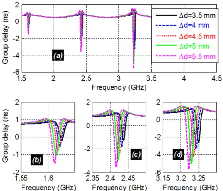
To get further insight about the influence of the cable length on the NGD circuit, parametric analyses are conducted. Fig. 2 depicts the schematic of the simulated structure. The tee-cable network was simulated in the SPICE schematic environment of the ADS® simulator from Keysight Technologies®. It is composed of ideal coaxial tees and cables. Th two identical connectors are defined by the characteristic impedance R0=50 Ω, physical length dc=4 mm and
relative permittivity εr=2. The two cables present the attenuation a=-0.3 dB and different lengths d and d+Δd.
Fig. 2. Schematic of the simulated tee-cable network.
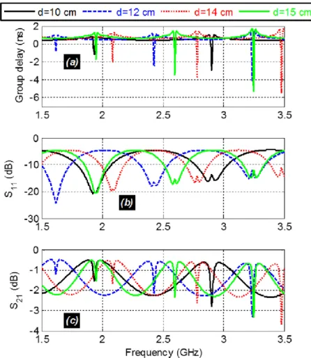
The present parametric analyses aim to illustrate the influence of the delays τ0 and Δτ. To gain more practical approach, the cable lengths are defined by the arbitrary chosen values d=0.12 m and Δd varied from 3.5 mm to 5.5 mm step 0.5 mm, and d varied from 0.1 m to 0.15 m step 0.02 m with Δd=4.5 mm. The structure S-parameters were simulated from 1.5 GHz to 3.5 GHz. The group delay and S-parameter frequency responses illustrating the influence of Δd are displayed in Fig. 3 and Fig. 4 respectively. The NGD center frequency decreases and the group delay level increases with the cable length difference Δd. It is seen that the tee-cable network enables to achieve a multiband NGD behaviors in the GHz frequency band. In addition, an outstanding NGD level better than -1 ns over the insertion loss better than 2 dB and reflection loss better than -15 dB in the NGD bandwidth. The group delay and S-parameter frequency responses illustrating the influence of d are displayed in Figs. 5.
Page 12 of 20
Fig. 3. Group delay response of the tee-cable network with the influence of Δd.
Page 13 of 20
Fig. 5. Group delay, transmission and reflection coefficients of the tee-cable network with the influence of d.
The NGD central frequency changes significantly with d as shown in Fig. 5(a). A frequency shift of the NGD multiband effect is observed. NGD level varying from about -1 ns to -6 ns in function of the central frequency position. Furthermore, as illustrated by Fig. 5(b) and Fig. 5(c), the insertion and return losses, respectively do not present notable change with length d.
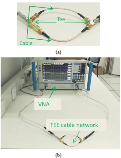
4.2 Description of Tee-cable POC
The photograph of the simple 50 Ω coaxial tee-cable POC prototype is exposed in Fig. 6(a). The tee and cable are classical instruments used in microwave measurement engineering implemented in SMA technology. The operated cable lengths are d≈0.125 m and Δd≈3.5 mm. They are built with concentric dielectric with relative permittivity
εr=2.3 and loss tangent tan(δ)≈0.01. The inner and outer radius of the dielectric insulating are about 3.44 mm and
6.76 mm. The constituting conductor element is a copper having thickness t=0.5 mm. The S-parameter measurements are completed using a VNA from Rohde & Schwarz (ZNB 20, frequency band 100 kHz to 20 GHz)
Page 14 of 20
which is shown in Fig. 6(b). The repeatability of this S-parameter experimentation is guaranteed like the measurement of classical microstrip circuits.
Fig. 6. Photographs of (a) the tested tee-cable prototype and (b) the measurement experimental setup.
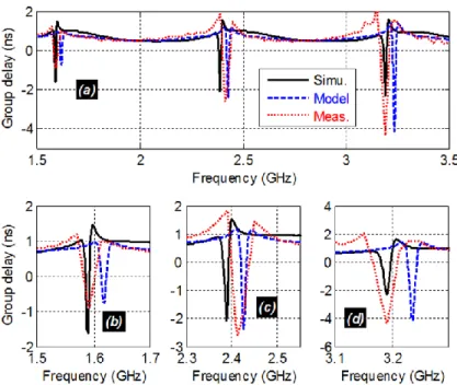
4.3 Discussion on simulated and measured results
The S-parameters of the tested tee-cable network were measured in the frequency band from 1.5 GHz to 3.5 GHz step 10 MHz. Figs. 7 show the comparisons between the theoretical model, simulation and measurement of the group delays. The particular frequency calculated from (30) is f0≈0.79 GHz. The modelled, simulated and measured results are in good agreement. Original tri-band NGD behaviour is observed at around 2f0≈1.58 GHz, 3f0≈2.42 GHz and 4f0≈3.19 GHz. As seen in Fig. 7, the NGD presenting optimal level of about -1 ns, -2 ns and -3 ns were observed around these frequencies respectively. However, the NGD bandwidths are particularly narrow band less than 12 MHz.
Page 15 of 20
Fig. 7. Comparison of the modeled, simulated and measured group delay of the tee-cable NGD POC prototypes shown in Fig. 6.
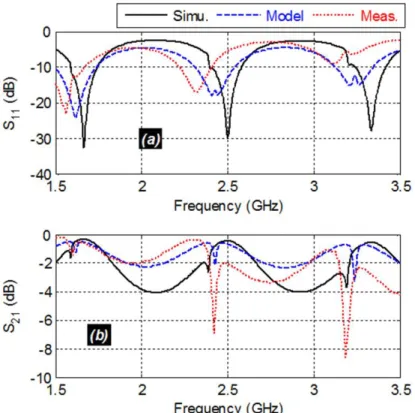
The measured NGD circuit enables to achieve insertion losses better than 1 dB and reflection loss better than 15 dB at the first NGD centre frequency as illustrated in Fig. 8. The obtained insertion loss is widely better compared to the existing NGD passive circuits. These theoretical, simulation and experimental results confirm the NGD concept feasibility with the tee-cable network-based topology. The discrepancies between the modelled, simulated and measured S-parameters can be caused by the fabrication imperfections, the tee and cable constituting material characteristic dispersions, the cable attenuation, which is assumed theoretically constant, changes with the frequency in function of the conductivity, and numerical inaccuracies of the simulator.
Page 16 of 20
Fig. 8. Comparison of the modeled, simulated and measured reflection and transmission coefficients of the tee-cable NGD POC prototype shown in Fig. 6.
The observed discrepancies between the calculated, simulated and measured results shown in Figs. 7 and in Figs. 8 are essentially caused by the following imperfections:
• Dispersions on the parameters of the cable substrate material, • Mismatch induced by the Tee cables/connectors (see Fig. 6),
• Numerical computation drifts of the full wave simulating tool, and of the calculated tool; this includes for instance the dispersion models and simulations constitutive parameters (geometrical, electrical ones).
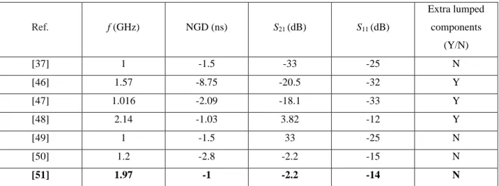
4.4 Comparison of NGD specifications with the state-of-the-art
We can understand from the comparative values of Table 2 the basic performances of the parallel cable structure topology under investigation and the existing ones available in the literature (see [37] and [46-51]). It can be underlined that the parallel cable NGD structure enable to achieve:
• Low signal attenuation in the NGD bandwidth,
• Reflection loss better than -14 dB in the NGD bandwidth,
• And it can be implemented with fully distributed elements without lossy lumped component. However, the parallel cable drawbacks are:
• The large size of the cable which is not easy to integrate in the printed circuit boards,
Page 17 of 20
Ref. f (GHz) NGD (ns) S21 (dB) S11 (dB) Extra lumped components (Y/N) [37] 1 -1.5 -33 -25 N [46] 1.57 -8.75 -20.5 -32 Y [47] 1.016 -2.09 -18.1 -33 Y [48] 2.14 -1.03 3.82 -12 Y [49] 1 -1.5 33 -25 N [50] 1.2 -2.8 -2.2 -15 N [51] 1.97 -1 -2.2 -14 NTable 2: Comparison of the NGD structure specifications and the available ones in the state-of-the-art.
4. CONCLUSION
An NGD analytical and experimental study on outstanding simple tee-cable network is investigated. The S-matrix model of the tee-cable equivalent circuit is developed. The NGD analysis is introduced in function of the cable parameter. The NGD theory validation is confirmed by calculations, simulations and experimentations. Parametric and numerical analyses of S-parameters in function of the cable length and attenuation are discussed. In addition, as POC, a tee-cable network prototype is tested. The theoretical prediction is verified with both simulations and measurements. It is demonstrated that the tested tee-cable generate a multiband NGD effect around GHz. In difference to the existing NGD passive circuits, the tee-cable NGD topology allows to achieve very low insertion loss, better than 2 dB and reflection loss better than 12 dB.
REFERENCE
[1] S.-S. Myoung, B.-S. Kwon, Y.-H. Kim and J.-G. Yook, “Effect of Group Delay in RF BPF on Impulse Radio Systems,” IEICE Tran. Communications, vol. 90, no. 12, 2007, pp. 3514-3522.
[2] B. L. Heffner, “Accurate, automated measurement of differential group delay dispersion and principal state variation using Jones matrix eigen analysis,” IEEE Photonics Technology Letters, Vol. 5, No. 7, July 1997, pp. 814-817.
[3] D.-H. Kwon, “Effect of Antenna Gain and Group Delay Variations on Pulse-Preserving Capabilities of Ultrawideband Antennas,” IEEE Trans. Antennas Propag., Vol. 54, No. 8, Aug. 2006, pp. 2208-2217.
Page 18 of 20
[4] B. Ravelo, “Delay modelling of high-speed distributed interconnect for the signal integrity prediction”, Eur. Phys. J. Appl. Phys., Vol. 57 (31002), Feb. 2012, pp. 1-8.
[5] X. Hu, X. Luan, S. Ren and J. Wu, “Propagation delays computation in GEO multi-beam satellite communications system,” in Proc. of 2012 International Conference on Systems and Informatics (ICSAI2012), Yantai, China, 19-20 May 2012, pp. 1631-1634.
[6] A. Weiss and E. Weinstein, “Fundamental limitations in passive time-delay estimation-Part I: Narrow-band systems,” IEEE Trans. on Acoustics, Speech, and Signal Processing, Vol. 31, No. 2, Apr. 1983, pp. 472-486. [7] E. Weinstein and A. Weiss, “Fundamental limitations in passive time-delay estimation-Part II: Wide-band
systems,” IEEE Trans.on Acoustics, Speech, and Signal Processing, Vol. 32, No. 5, Oct. 1984, pp. 1064-1078. [8] P. Ziska and J. Vrbata, “Method for design of analog group delay equalizers,” in Proc. of 2006 IEEE
International Symposium on Circuits and Systems, Island of Kos, Greece, 21-24 May 2006, pp. 445-448. [9] P. Žiska and M. Laipert, “Analog Group Delay Equalizers Design Based on Evolutionary Algorithm,”
Radioengineering, Vol. 15, No. 1, Apr. 2006, pp. 1-5.
[10] S. Gupta, A. Parsa, E. Perret, R. V. Snyder, R. J. Wenzel and C. Caloz, “Group-Delay Engineered Noncommensurate Transmission Line All-Pass Network for Analog Signal Processing,” IEEE Trans. Microw. Theory Techn., Vol. 58, No. 9, Sept. 2010, pp. 2392-2407.
[11] G. Pasolini and R. Soloperto, “Multistage Decimators with Minimum Group Delay,” 2010 IEEE International Conference on Communications, Cape Town, South Africa, 23-27 May 2010, pp. 1-6.
[12] P. Keerthan and K. J. Vinoy, “Design of cascaded all pass network with monotonous group delay response for broadband radio frequency applications,” IET Microwaves, Antennas & Propagation, Vol. 10, No. 7, May 2016, pp. 808– 815.
[13] B. Ravelo, “Neutralization of LC- and RC-Effects with Left-Handed and NGD Circuits”, Advanced Electromagnetics (AEM), Vol. 2, No. 1, Sept. 2013, pp. 73-84.
[14] C. D. Broomfield and J. K. A. Everard, “Broadband Negative Group Delay Networks for Compensation of Oscillators, Filters and Communication Systems,” Electron. Lett., Vol. 23, pp. 1931-1933, Nov. 2000.
[15] S. S. Oh and L. Shafai, “Compensated circuit with characteristics of lossless double negative materials and its application to array antennas,” IET Microw. Antennas Propag., Vol. 1, No. 1, Feb. 2007, pp. 29-38.
[16] A. I. Abunjaileh and I. C. Hunter, “A matched bridged tee network with positive phase derivative,” Digest MTT-S International Microwave Symposium, 2011 Baltimore, MD, USA, 5-10 June 2011, pp. 1-4.
[17] H. Choi, Y. Jeong, C. D. Kim, and J. S. Kenney, “Efficiency enhancement of feedforward amplifiers by employing a negative group delay circuit,” IEEE Trans. Microw. Theory Tech., Vol. 58, No. 5, May 2010, pp. 1116–1125.
[18] H. Choi, Y. Jeong, C. D. Kim, and J. S. Kenney, “Bandwidth enhancement of an analog feedback amplifier by employing a negative group delay circuit,” Progress In Electromagnetics Research, Vol. 105, 2010, pp. 253-272. [19] M. Kandic and G. E. Bridges, “Bilateral gain-compensated negative group delay circuit,” IEEE MWC Lett., Vol.
21, No. 6, pp. 308-310, June 2011.
[20] G. E. Bridges and M. Kandic, “Gain compensated symmetric loaded transmission line exhibiting bidirectional negative group delay,” Applied Physics A, Vol. 109, No. 4, Dec. 2012, pp. 1087–1093.
Page 19 of 20
[21] Y. Meng, Z. Wang, S. Fang, T. Shao and H. Liu, “A Broadband Switch-Less Bi-Directional Amplifier with Negative-Group-Delay Matching Circuits,” Electronics, Vol. 7, No. 158, Aug. 2018, pp. 1-11.
[22] C.-T. M. Wu, S. Gharavi, B. Daneshrad, and T. Itoh, “A Dual-Purpose Reconfigurable Negative Group Delay Circuit Based on Distributed Amplifiers,” IEEE MWC Lett., Vol. 23, No. 11, pp. 593-595, Nov. 2013.
[23] H. Mirzaei and G. V. Eleftheriades, “Arbitrary-angle squint-free beamforming in series-fed antenna arrays using non-Foster elements synthesized by negative-group-delay networks,” IEEE Trans. Antennas Propag., Vol. 63, No. 5, May 2015, pp. 1997-2010.
[24] Y. Wu, H. Wang, Z. Zhuang, Y. Liu and Q. Xue, “A Novel Arbitrary Terminated Unequal Coupler With Bandwidth-Enhanced Positive and Negative Group Delay Characteristics,” IEEE Trans. Microw. Theory Techn., Vol. 66, No. 5, May 2018, pp. 2170-2184.
[25] A. Mortazawi and W. Alomar, “Negative group delay circuit,” United States Patent Application, US20160093958, Mar. 2016.
[26] M. Bao and Y. Su, “Device for negative group delay,” United State Patent, US9419586 B2/WO 2014029412 A1, Aug. 2016.
[27] B. Ravelo, “Demonstration of negative signal delay with short-duration transient pulse”, Eur. Phys. J. Appl. Phys. (EPJAP), Vol. 55 (10103), 2011, pp. 1-8.
[28] R. Zakarevicius, “Group Delay Estimation with Wideband Signals,” IEEE Trans. on Communications, Vol. 27, No. 12, Dec. 1979, pp. 1908-1910.
[29] B. Yegnanarayana, D. Saikia and T. Krishnan, “Significance of group delay functions in signal reconstruction from spectral magnitude or phase,” IEEE Transactions on Acoustics, Speech, and Signal Processing, Vol. 32, No. 3, June 1984, pp. 610-623.
[30] S. Lucyszyn, and I. D. Robertson, “Analog Reflection Topology Building Blocks for Adaptive Microwave Signal Processing Applications,” IEEE Trans. Microwave Theory Techn., Vol. MTT-43, No. 3, Mar. 1995, pp. 601-611.
[31] S. Lucyszyn, I. D. Robertson, and A. H. Aghvami, “Negative Group Delay Synthesiser,” Electron. Lett., Vol. 29, pp. 798-800, Apr. 1993.
[32] G. V. Eleftheriades, O. Siddiqui, and A. K. Iyer, “Transmission Line for Negative Refractive Index Media and Associated Implementations without Excess Resonators,” IEEE MWC Lett., Vol. 13, No. 2, pp. 51-53, Feb. 2003.
[33] O. F. Siddiqui, M. Mojahedi, and G. V. Eleftheriades, “Periodically Loaded Transmission Line with Effective Negative Refractive Index and Negative Group Velocity,” IEEE Trans. Antennas Propag., Vol. 51, No. 10, pp. 2619-2625, Oct. 2003.
[34] O. F. Siddiqui, S. J. Erickson, G. V. Eleftheriades, and M. Mojahedi, “Time-Domain Measurement of Negative-Index Transmission-Line Metamaterials,” IEEE Trans. Microw. Theory Techn., Vol. 52, No. 5, pp. 1449-1453, May 2004.
[35] M. Kandic and G. E. Bridges, “Asymptotic Limits of Negative Group Delay in Active Resonator-Based Distributed Circuits,” IEEE Transactions on Circuits and Systems I: Regular Papers, Vol. 58, No. 8, Aug. 2011, pp. 1727-1735.
Page 20 of 20
[36] H. Mirzaei and G. V. Eleftheriades, “Realizing Non-Foster Reactive Elements Using Negative-Group-Delay Networks,” IEEE Trans. Microw. Theory Tech., Vol. 61, No. 12, Dec. 2013, pp. 4322-4332.
[37] C.-T. M. Wu and T. Itoh, “Maximally Flat Negative Group-Delay Circuit: A Microwave Transversal Filter Approach,” IEEE Trans. Microw. Theory Techn., Vol. 62, No. 6, pp. 1330-1342, Apr. 2014.
[38] J. J. Barroso, J. E. B. Oliveira, O. L. Coutinho and U. C. Hasar, “Negative group velocity in resistive lossy left-handed transmission lines,” IET Microwaves, Antennas & Propagation, Vol. 10, No. 7, May 2016, p. 808 – 815. [39] G. Chaudhary, Y. Jeong, and J. Lim, “Microstrip Line Negative Group Delay Filters for Microwave Circuits,”
IEEE Trans. Microw. Theory Techn., Vol. 62, No. 2, pp. 234-243, Feb. 2014.
[40] G. Chaudhary and Y. Jeong, “Distributed Transmission Line Negative Group Delay Circuit with Improved Signal Attenuation,” IEEE MWC Lett., Vol. 24, No. 1, pp. 20-22, Jan. 2014.
[41] G. Liu, and J. Xu, “Compact transmission-type negative group delay circuit with low attenuation,” Electronics Letters, Vol. 53, No. 7, Mar. 2017, pp. 476-478.
[42] B. Ravelo, “Negative Group-Delay Phenomenon Analysis with Distributed Parallel Interconnect Line,” IEEE Trans. Electromagn. Compat., Vol. 58, No. 2, pp. 573-580, Apr. 2016.
[43] B. Ravelo, “Tee power divider and combiner based negative group delay topology”, International Journal of RF and Microwave Computer-Aided Engineering, Vol. 28, No. 9, Nov. 2018, pp. 1-9.
[44] B. Ravelo, “Theory on Coupled Line Coupler-Based Negative Group Delay Microwave Circuit,” IEEE Trans. Microw. Theory Techn., Vol. 64, No. 11, pp. 3604-3611, Nov. 2016.
[45] R. Das, Q. Zhang and H. Liu, “Lossy Coupling Matrix Synthesis Approach for the Realization of Negative Group Delay Response,” IEEE Access, Vol. 6, Dec. 2017, pp. 1916-1926.
[46] T. Shao, Z. Wang, S. Fang, H. Liu, and S. Fu, “A compact transmission line self-matched negative group delay microwave circuit,” IEEE Access, vol. 5. pp. 22836–22843, Oct. 2017.
[47] Z. Wang, Y. Cao, T. Shao, S. Fang and Y. Liu, “A Negative Group Delay Microwave Circuit Based on Signal Interference Techniques,” IEEE Microw. Wireless Compon. Lett., vol. 28, no. 4, pp. 290-292, Apr. 2018. [48] G. Chaudhary and Y. Jeong, “Negative group delay phenomenon analysis using finite unloaded quality factor
resonators,” Prog. Electromagn. Res., vol. 156, pp. 55–62, Jun. 2016.
[49] G. Chaudhary and Y. Jeong, “Transmission-type negative group delay networks using coupled line doublet structure,” IET Microw. Antennas Propag., vol. 9, no. 8, pp. 748-754, Jun. 2015.
[50] F. Wan, N. Li, B. Ravelo, J. Ge, “O=O Shape Low-Loss Negative Group Delay Microstrip Circuit”, IEEE Transactions on Circuits and Systems II: Express Briefs, Early access, 2020, pp. 1-5, 2019.
[51] F. Wan, N. Li, B. Ravelo, N. M. Mourad and W. Rahajandraibe, “NGD Analysis of Turtle-Shape Microstrip Circuit”, IEEE Transactions on Circuits and Systems II: Express Briefs, Early access, pp. 1-5, 2020.