HAL Id: hal-02974746
https://hal.archives-ouvertes.fr/hal-02974746
Submitted on 22 Oct 2020
HAL is a multi-disciplinary open access archive for the deposit and dissemination of sci-entific research documents, whether they are pub-lished or not. The documents may come from teaching and research institutions in France or abroad, or from public or private research centers.
L’archive ouverte pluridisciplinaire HAL, est destinée au dépôt et à la diffusion de documents scientifiques de niveau recherche, publiés ou non, émanant des établissements d’enseignement et de recherche français ou étrangers, des laboratoires publics ou privés.
Influence of dielectric layer thickness on charge
injection, accumulation and transport phenomena in
thin silicon oxynitride layers: a nanoscale study
Florian Mortreuil, Laurent Boudou, K Makasheva, G. Teyssedre, Christina
Villeneuve-Faure
To cite this version:
Florian Mortreuil, Laurent Boudou, K Makasheva, G. Teyssedre, Christina Villeneuve-Faure. In-fluence of dielectric layer thickness on charge injection, accumulation and transport phenomena in thin silicon oxynitride layers: a nanoscale study. Nanotechnology, Institute of Physics, 2021, 32 (6), pp.065706. �10.1088/1361-6528/abc38a�. �hal-02974746�
1
Influence of dielectric layer thickness on charge injection, accumulation
and transport phenomena in thin silicon oxynitride layers: a nanoscale
study
F. Mortreuil, L. Boudou, K. Makasheva, G. Teyssedre and C. Villeneuve-Faure*
LAPLACE (Laboratoire Plasma et Conversion d’Energie), Université de Toulouse; CNRS UPS, INPT; 118 route de Narbonne, F-31062 Toulouse cedex 9, France.
*Corresponding author: christina.villeneuve@laplace.univ-tlse.fr
Abstract
Charge injection and retention in thin dielectric layers remain critical issues due to the great number of failure mechanisms they inflict. Achieving a better understanding and control of charge injection, trapping and transport phenomena in thin dielectric films is of high priority aiming at increasing lifetime and improving reliability of dielectric parts in electronic and electrical devices. Thermal silica is an excellent dielectric but for many of the current technological developments more flexible processes are required for synthesizing high quality dielectric materials such as amorphous silicon oxynitride layers using plasma methods. In this article, the studied dielectric layers are plasma deposited SiOxNy. Independently on the layer thickness, they are structurally identical: optically transparent, having the same refractive index, equal to the one of thermal silica. Influence of the dielectric film thickness on charging phenomena in such layers is investigated at nanoscale using Kelvin Probe Force Microscopy (KPFM) and Conductive Atomic Force Microscopy (C-AFM). The main effect of the dielectric film thickness variation concerns the charge flow in the layer during the charge injection step. According to the SiOxNy layer thickness two distinct trends of the measured surface potential and current are found, thus defining ultrathin (up to 15 nm thickness) and thin (15 nm – 150 nm thickness) layers. Nevertheless, analyses of KPFM surface potential measurements associated with results from Finite Element Modelling of the structures show that the dielectric layer thickness has weak influence on the amount of injected charge and on the decay dynamics, meaning that pretty homogeneous layers can be processed. The charge penetration depth in such dielectric layers is evaluated to 10 nm regardless the dielectric thickness.
Keywords: thin film, dielectric, plasma deposition, charge injection, Kelvin Probe Force Microscopy, space charge
2
1. Introduction
Common property of the dielectric materials is to accumulate charges under external stress, either electric field or particle beam irradiation. Charge accumulation phenomena occur in any dielectric regardless its dimensions (centimeter or nanometer scale) inducing inhomogeneous internal electric field. Even though this effect lies down the principle of operation of a large number of applications as non-volatile memory devices [1, 2] it causes dielectric troubleshoots in other devices like electrostatic adhesion in MicroElectroMechanical System (MEMS) [3] or induces damages in electronic devices through uncontrolled electrostatic discharges [4]. Thus, the dielectric charging phenomenon appears as one of the major challenges to meet for many electrical systems. The mechanisms of charge injection and accumulation in dielectric layers remain constantly a subject of scientific research aiming at a better managing of this phenomenon and controlling the level of electrostatic charging of the dielectric layers [1, 2, 5-7]. However, major advances on the matter can be expected after development of appropriate diagnostic to probe charge injection and decay in thin dielectric layers.
During the past decades, a lot of experimental techniques have been developed to measure space charge distribution as function of the depth in the dielectric and the question of their adaptation to thin dielectrics was raised [8, 9]. These techniques, based on acoustic or thermal interaction with electrical charges, provide charge density distribution in thick polymer films (thickness from few tens up to few cents of micrometers) with spatial resolution approaching 1µm but they fail to probe charge injection and decay mechanisms in thin dielectric films (thickness in the nanoscale range) used in electronic or microsystems components. Moreover, when the layer thickness scales down the micrometer range, specific issues like interfaces or transition between amorphous and crystalline domains in the dielectric, especially for insulating polymers, are superimposed [10].
Aiming at a study of the charges distribution in thin dielectric films, techniques derived from Scanning Probe Microscopy (SPM) have naturally emerged to inject locally charges and to image the resulting surface potential modification. In this case, the Atomic Force Microscope (AFM) tip is used to perform local charge injection in dielectric materials, followed by measurements of the induced resonance frequency shift by Electrostatic Force Microscopy (EFM) [11-14] or by the resulting surface potential in Kelvin Probe Force Microscopy (KPFM) [5, 11, 15]. Literature overview emphasizes that charge injection and decay in thin dielectric films were extensively studied by EFM and KPFM focusing on charge density determination [16, 17], influence of the experimental conditions (humidity [5, 11, 18], lift height [19] or perturbation introduced by the electrostatic forces [20, 21]), or charge dynamics [11, 19]. In
3
spite of the numerous investigations on the problem, many aspects as charges distribution within the layer, mechanisms occurring at the metal/dielectric interface or charge injection mechanisms remain currently ill described. Besides, the AFM techniques can bring complementary information on the dielectric charging phenomenon. For example, low-current measurements in thin dielectric layers can be performed by conductive-AFM (C-AFM) or Tunneling AFM (TUNA) [22]. Two aspects can be thus investigated: (i) dielectric reliability in terms of breakdown [23] or leakage current [24] and (ii) mechanisms occurring during charge injection and transport. It was demonstrated for ultrathin SiO2 layer (less than 4 nm) that Fowler-Nordheim mechanism [23, 25] can be extracted from current versus voltage curves. However, determination of some physical parameters as energy barrier or in-depth charge distribution remains strongly correlated to the tip-sample surface contact estimation [25-29] and requires alternative approaches.
This paper is dedicated to an experimental study of the influence of dielectric layer thickness on charge injection and transport in thin amorphous silicon oxynitride layers. This well-characterized material [30, 31], elaborated by plasma process, presents electrical properties very close to those of thermal silica which makes it perfect model material. Surface potential measurements achieved by KPFM and current measurements performed by C-AFM are combined to better understand charge injection mechanisms in thin dielectric films. The paper is organized as follows: the experimental details are presented in section 2. Section 3 is dedicated to results and discussion focusing successively on the SiOxNy layers characterization, the influence of dielectric thickness on charge injection mechanism and the amount of injected charges, the current versus voltage characteristics recorded by C-AFM, and the charge dynamics after injection. Finally, Section 4 summarizes the main conclusions.
2. Experimental
Plasma processed amorphous silicon oxynitride layers (SiOxNy) with very low N-content (of only 4 at. %) have been chosen for this study because of their outstanding electrical properties, close to those of thermal silica, and the possibility to well-control their thickness [30]. The dielectric layers were deposited by Pulsed Plasma Enhanced Chemical Vapor Deposition (PPECVD) in a radio-frequency (RF) capacitively coupled discharge sustained at low gas pressure. The parameters of the plasma process are summarized in Table 1. The gas mixture was of He, SiH4 and N2O, with helium as a vector gas (39.7% of the total gas flow). The N2O content was high, in order to achieve good quality silica layers. The RF discharge was modulated with square pulses to avoid dust formation in the plasma and to improve quality of
4
the deposited layers, thus their dielectric properties. The arrangement of the dielectric matrix, and accordingly the quality of deposited silica layers was further improved by the very slow deposition process and the high temperature of the substrate during deposition. More details on the plasma process are presented elsewhere [30,31].
Table 1. Parameters of the plasma process for deposition of SiOxNy-layers and the dry oxidation process for growth of thermal SiO2-base.
Plasma conditions for deposition of SiOxNy-layers
RF frequency 13.56 MHz
Applied power 5 W
Pulse period 400 ms
Pulse width 100 ms
Total pressure 65 Pa
Total gas flow 201.2 sccm
He flow 80 sccm
N2O flow 120 sccm
SiH4 flow 1.2 sccm
Precursor ratio, = [N2O]/[SiH4] 100
Deposition rate 3.9 nm/min
Substrate temperature 300°C
Dry oxidation conditions for growth of thermal SiO2-base
Total pressure 1030 hPa
Gas mixture N2-O2
O2-content 1%
Temperature 1100°C
The structure of the studied devices is shown in figure 1. The basis consists of a 50 nm-thick SiO2 layer thermally grown on Si (100) intrinsic substrates by dry oxidation. The parameters of the dry oxidation process are given in Table 1. 70 nm-thick Au/Ti-electrodes (60 nm of Au and 10 nm of Ti with the Ti-layer used as adhesion layer) were processed by sputtering on top of the basis SiO2 by sputtering. Two kinds of metal electrodes were designed: large square plate (4 × 4 mm2) floating electrode for charge injection study (figure 1(a)) and small wire (40 µm width and 1 mm long) localized electrode for current measurements (figure 1(b)). Top view of the wire electrode is shown on the Scanning Electron Microscopy image (figure 1(c)). To embed the metal electrodes at different depths the structures were covered by
5
SiOxNy dielectric layers with different thicknesses as top layers. The thickness of the dielectric top SiOxNy-layers was controlled by the deposition time according to the characteristic for the system low deposition rate. After the SiOxNy deposition a small opening in the top dielectric layer was made to reach the Au-electrode for the current measurements (figures 1(b) and 1(c)). Spectroscopic ellipsometry was used to measure the dielectric layer thicknesses according to the procedure developed earlier [31]. A SOPRA GES-5 ellipsometer with a rotating polarizer and a fixed analyzer was used in the spectral range 250–850 nm. The simulation of the recorded spectra was performed with Winelli software provided by SOPRA LAB [32]. Forouhi-Bloomer dispersion law was applied for the spectra processing [33]. This approximation applies for dielectric and semiconducting thin layers and provides information on the layer thickness and optical properties (n – refractive index and k – extinction coefficient). AFM measurements were performed using a Bruker Multimode 8 apparatus under controlled environment (without humidity since under N2 atmosphere) to avoid charge dissipation due to the presence of water layer on the sample surface [31]. A silicon AFM tip with PtIr coating (curvature radius Rc = 25 nm and spring constant ks = 2.4 N/m) was used for the charge injection protocol and for the surface potential measurements by KPFM. The dielectric charging was achieved in contact mode (contact force set to 90 nN) by applying positive DC bias (V0 = +5 to +15 V) to the AFM tip for different time durations, the sample back side being grounded (figure 1(a)). After the charging step, the same tip was used to probe the surface potential in Amplitude Modulation KPFM mode using a 10 nm-lift.
Current measurements were performed with a diamond coated highly doped Si tip (Rc = 125 nm and ks = 2 N/m) using C-AFM mode (figure 1(b)). A bias varying between +1 V and +20 V was applied to the Au-electrode. In order to adapt the noise detection level, the current measurements were performed owing to a low noise amplifier module, with 20 pA-sensitivity for the dielectric layers thicker than 15 nm and 10 nA-pA-sensitivity for lower thicknesses. Current was acquired during 60 s for each bias.
6 Figure 1. The studied device is composed of thermal SiO2 base, Au electrode and SiOxNy-layer over Si substrate. Device configuration for (a) charge injection and decay measurements and (b) C-AFM measurement; (c) Scanning Electron Microscopy top view image of the Au-electrode embedded at 31 nm for the current measurements.
3. Results and discussion
3.1 Dielectric layer characterization
The thickness and optical parameters of the plasma deposited SiOxNy layers were systematically measured by spectroscopic ellipsometry. The SiOxNy-layers span in the thickness range from ultrathin, i.e. up to 15 nm (5.9 ± 0.4 nm and 11.1 ± 0.9 nm) to thin, 15 nm < d < 150 nm (15.6 ± 0.4 nm, 31.1 ± 0.2 nm, 50.0 ± 0.2 nm, 68.0 ± 0.3 nm, 129.7 ± 0.8 nm), layers. They are all transparent with extinction coefficient k < 0.002 in the investigated spectral range, having refractive index n = 1.45 ± 0.1 at wavelength = 632.8 nm (figure 2) which qualifies them as layers with optical properties very close to thermal silica layers. Using the Forouhi-Bloomer dispersion law for spectra processing allows for extraction of the layer thickness and the optical properties in a consistent way. It avoids overestimation of the layer thickness when the refractive index of bulk silica is applied for simulation of the recorded ellipsometric spectra [34]. Regardless the SiOxNy-layer thickness the refractive index remains the same (figure 2(a)). We do not observe departure in the optical properties, towards higher refractive index, for the ultrathin SiOxNy-layers as reported for ultrathin SiO2 thermal layers [34]. Conservation of the refractive index for the SiOxNy-layers is most likely due to the plasma deposition process for which the layer growth results from deposition of plasma generated radicals, issued from the injected precursors. The applied for this study pulsed mode of operation of the PPECVD process improved the quality of the deposited layer. It leads to homogeneous distribution of the gas precursors in the reactor between the pulses, before each plasma ignition, which prevents from plasma deposition under O-related by-products exhaust [35]. Thus the PPECVD process allows for better control of the layer stoichiometry (O / Si = 2), avoiding modifications in the layer composition and structure.
400µm Au (c) Si (a) d Floating Au electrode Injected charge Si (b) Au electrode d A th-SiO2 th-SiO2 SiOxNy SiOxNy
7 Figure 2. (a) Refractive index and extinction coefficient of the studied SiOxNy thin dielectric layers as obtained from spectroscopic ellipsometry at = 632.8 nm, (b) Variation of the refractive index and the extinction coefficient in the studied wavelength range for one ultrathin SiOxNy layer (d = 11.1 nm) and one thin layer (d = 129.7 nm).
The spectral response of the SiOxNy-layers is closely related to the dielectric structure of the layer. It also gives information on the energy gap and the different charge traps [36]. After processing of the ellipsometry spectra, for all studied here SiOxNy-layers, we have found an electronic part of the dielectric constant of = 2.13 (n = 1.46). The later provides a Schottky pinning parameter of Sp = 0.887 and defines the charge state in the SiOxNy dielectric interface as slightly pinned when in contact with a metal electrode [36, 37]. A small increase of the refractive index is observed in the Mid-UV and Near-UV range for the thickest SiOxNy layer (d = 129.7 nm, in figure 2(b)). In addition to the normal dispersion of the refractive index in that spectral region, the refractive index increase is most likely due to the limited, but present small N-content (4 at. %) in the SiOxNy-layer.
3.2. Impact of the dielectric thickness on the charge injection: KPFM study
For each SiOxNy layer, charge injection was done under tip bias V0 varying from +5 V to +15 V during various times (from 1 min to 10 min). Immediately after charge injection, the KPFM
0 20 40 60 80 100 120 140 1.40 1.45 1.50 ref rac tiv e index - n SiO xNy layer thickness (nm) at = 632.8 nm 0.000 0.005 0.8 1.0 e x tin c tio n c oe ffic ie nt - k 200 300 400 500 600 700 800 900 1.40 1.45 1.50 d = 11.1 nm d = 129.7 nm (a) = 632.8 nm ref rac tiv e index - n Wavelength (nm) (b) 0.000 0.005 0.8 1 e x tin c tio n c oe ffic ie nt - k
8
surface potential profiles were recorded along a line crossing the injection point (figure 3) [31]. Figure 3(a) represents the surface potential induced by the injected charges. The potential distribution is of round shape. AFM mapping of the SiOxNy-surface in the region of charge injection shows no modification of the SiOxNy-surface topography (figure 3(b)). A classical Gaussian shape of the potential profile is observed (figure 3(c)). Three relevant parameters were extracted from this profile: (i) The maximum potential Vm, with respect to surface reference potential, which is measured at the injection point; (ii) The Full Width at Half Maximum (FWHM) which reflects the charges lateral spreading and (iii) The area IS under the potential profile which is considered to represent, to a first approximation, the quantity of stored charges. The later assumption is considered valid even for thin dielectric films because the injected charges remain close to the surface. The evolution of these three parameters, as function of the charge injection conditions, was investigated to follow the charge injection and transport dynamics. The reference potential in figure 3(c) corresponds to the potential of the surface prior to charge injection. Reproducibility measurements show very low variation in the probed values of the potential profile, thus the extracted parameters. Standard deviation of the potential maximum does not exceed 8% and the one of FWHM of the potential profile is limited to 4%. For clarity issues errors bars are not represented on the figures later on.
Figure 3. AFM mapping of the SiOxNy-surface in the region of charge injection (2 min at V0 = +12 V) for the 130 nm-thick layer: (a) potential distribution and (b) SiOxNy surface topography. (c) KPFM surface potential profile.
Figure 4(a) represents the evolution of the surface potential profile as function of the film thickness for charge injection at +12 V during 2 min. One can distinguish two different trends with respect to the dielectric layer thickness.
- Dielectric layers with thickness less than 15 nm (ultrathin layers): FWHM and area IS increase with the dielectric layer thickness even though the electric field decreases (constant bias voltage).
-2 -1 0 1 2 0.0 0.5 1.0 1.5 2.0 V m KPFM surfa ce p otenti al (V) Lateral position (µm) Reference potential FWHM (c) 0 2 4 0 1 2 3 Position (µm) P o te n tie l (V ) FWHM (a) (b) (c) 0 1 2 3 1 µm (b) 0 2 4 0 1 2 3 Position (µm) P o te n tie l (V ) FWHM (a) (b) (c) 0 1 2 3 1 µm (a)
9
- Dielectric layers with thickness larger than 15 nm (thin layers): FWHM and area IS are insensitive to the dielectric layer thickness.
The influence of the dielectric thickness on the evolution of the maximum potential Vm and area IS as function of the injection time for different SiOxNy-layer thicknesses is presented in figure 4(b). As previously, different behaviors are observed as function of the dielectric layer thickness for ultrathin and thin layers. For the 11 nm-thick SiOxNy-layer, IS and Vm remain relatively constant regardless the injection time. The 31 nm-thick SiOxNy behaves differently for short and longer injection times. For short times (less than 5 min), Vm and IS increase with injection time. For longer injection times a saturation in the two parameters is observed. As for the 130 nm-thick SiOxNy-layer, the Vm and IS increase with the injection time but the FWHM (not shown vs. charging time) of the potential profile is slightly influenced by the injection time. It increases by only 0.1 µm, from 0.4 µm for 1 min charging time to 0.5 µm for 10 min.
Figure 4. (a) Evolution of the surface potential profile FWHM and area IS as function of the SiOxNy-layer thickness for constant injection time and bias (2 min at V0 = +12 V); (b) Evolution of the surface potential maximum Vm and the area IS under peak as function of the injection time for SiOxNy-layers with different thicknesses (applied bias of V0 = +12 V).
The same evolution of the surface potential profile is observed when increasing the injection bias for a fixed injection time (results not shown). Indeed, the Vm and IS are insensitive to the injection bias increase for charge injection in the 11 nm-thick film, whereas these two parameters increase with increasing the bias for charge injection in the 130 nm-thick dielectric film. Concerning the 31 nm-thick film, again a two steps behavior is observed: the increase of Vm and IS with increasing the injection bias is followed by saturation (for applied bias larger than +8 V). However, the relationship between the area and the amount of injected charges is not straightforward in this case because of the dielectric layer thickness. This aspect will be discussed in detail in the following sections.
0 20 40 60 80 100 120 140 0.0 0.2 0.4 0.6 0.8 1.0 FWH M (µm ) SiO xNy thickness (nm) (a) 0.0 0.2 0.4 0.6 0.8 1.0 A rea I S (Vµm ) 0 2 4 6 8 10 0 1 2 3 4 Max imum po ten tial V m (V)
Injection time (min)
Maximum 11nm 31nm 130nm (b) 0 1 2 3 4 Ar ea I S (Vµ m) Area 11nm 31nm 130nm
10
3.3. Electric field influence on the charge injection: modeling approach
Results presented in the previous part show different fate of the injected charges depending on the dielectric layer thickness. To better understand the underlying mechanisms, we have performed an electrostatic modelling of the system aiming at identification of the relative contribution of the electric field components during charge injection and the influence of dielectric layer thickness on the surface potential profile.
The electric field is computed using a simple model consisting in a truncated cone of 10 µm-height with 14° aperture angle, ending with a semi-spherical apex of Rc = 25 nm or Rc = 125 nm. The considered geometry corresponds to a classical AFM tip shape used for modelling [38]. It accounts for the macroscopic shape of the tip, rather than the nanoscopic shape of the tip apex due to the long range nature of the electrostatic forces [39]. This tip is surrounded by an air box (dimensions large enough to avoid edge effects). It is in contact with the dielectric SiOxNy layer (figure 5(a)). The Au-electrode is considered at floating potential. Potential and electric field are computed in air, SiOxNy, SiO2 layers and in the intrinsic Si-substrate. The electric field is supposed capacitively distributed considering the relatively short polarization times used here and the large dielectric time constant for the dielectric layers. The relative dielectric permittivity of the SiOxNy layer is taken r = 3.9, as measured by dielectric spectroscopy for the very same dielectric layers [30]. For the thermal SiO2 and the Si-substrate it is r = 3.9 and 12, respectively. The model is 2D-axisymmetric based on Finite-Element Model (FEM) developed on COMSOL Multiphysics. The mesh is refined and optimized close to the contact point to improve calculation accuracy. The potential is applied on the tip and the ground is taken at the silicon substrate backside (charge injection configuration). The dielectric is supposed free from charges at the initial state. The boundary conditions are selected to ensure no edge effect and no charges (zero potential) on the free boundaries of the simulation box.
The Poisson's equation is solved in air and in the dielectric layers to determine the potential V.
∇
⃗⃗ ∙ (𝜀0𝜀𝑟𝐸⃗ ) = 𝜌 (1) where ρ is the charge density and ε0 is the vacuum permittivity.
The electric field 𝐸⃗ is derived from the potential V:
11 Figure 5. (a) Scheme of the AFM tip and the sample system, (b) Spatial distribution of computed electric field modulus for V0 = +10 V applied to the tip during charging protocol (Rc = 25 nm) for the 130 nm-thick dielectric layer, (c) Related Ez electric field in-depth distribution of the 130 nm-thick dielectric layer. In insert, the Ez in-depth distribution of the 130 nm-thick and the 11 nm-thick dielectric layer for the same V0 and (d) the lateral Er electric field distribution at the dielectric/air interface of the 130 nm-thick dielectric layer. In insert, the lateral Er distribution of the 130 nm-thick and the 11 nm-thick dielectric layer for the same V0.
The electric field distribution in the 130 nm-thick SiOxNy dielectric layer for a bias of V0 = +10 V applied to the tip in charge injection configuration is depicted in figure 5(b). The electric field is non-homogeneously distributed in the dielectric layer. An electric field strengthening is observed at the contact point under the tip. The electric field is substantially enhanced close to the injection area compared to the electric field strength in plane-plane configuration for the same dielectric thickness.
The in-depth evolution of the Ez-component of the electric field along the revolution axis is represented in figure 5(c) for the 130 nm-thick and the 11 nm-thick (insert of figure 5(c)) dielectric layers. The Ez-field decreases exponentially in the 130 nm-thick dielectric layer. The Ez-field decrease is reduced in the 11 nm-thick layer. The more homogeneous in-depth
0 20 40 60 80 100 120 140 0 1 2 3 d = 130 nm Lateral position r (nm) E r (z=0) (10 7 V/ m ) (d) 0 40 80 120 0 1 2 3 d = 130 nm Lateral position r (nm) Er (z =0 ) (10 7 V/m ) d = 11 nm 0 20 40 60 80 100 120 140 0 2 4 6 8 d = 130 nm In-depth position z (nm) E z (r=0 ) ( 10 7 V/ m ) (c) 0 4 8 0 4 8 d = 130 nm In-depth position z (nm) Ez (r=0 ) (10 7 V/m ) d = 11 nm
12
distribution of the electric field in the 11 nm-thick layer is explained by the fact that for dielectric layers with thicknesses smaller than the AFM tip radius, the configuration gets closer to a plane-plane one. In our configuration this effect is ensured by the Au layer, which screens the electric field, and diminishes the influence of the thermal SiO2 layer and the intrinsic Si bulk. The evolution of the lateral Er-component of the electric field along the dielectric surface is represented in figure 5(d) for the 130 nm-thick and the 11 nm-thick (insert of figure 5(d)) dielectric layers. One can notice that the maximum lateral electric field is less influenced by the thickness of the dielectric layer whereas a profile broadening is observed for the thinner layer. This high lateral electric field drives the charges spreading in radial direction.
Figure 6. Evolution of surface potential maximum Vm and FWHM as function of the SiOxNy film thickness for an electric field at the injection point of 4.7 × 10⁷ V/m (injection time of 2 min).
The strong inhomogeneity of the electric field, especially for thin SiOxNy-layers (d > 15 nm) prevents from correct interpretation of the measured surface potential on films of different thicknesses, as the electric field at the contact point is different. For comparison reasons figure 6 represents the variation of the surface potential maximum Vm and FWHM as function of the film thickness for the same initial electric field at the injection point, as calculated from the above described model. The FWHM does not vary significantly with the dielectric layer thickness. This is most probably related to the fact that the lateral electric field maximum is weakly influenced by the dielectric layer thickness (figure 5(d)). In addition, it is of the order of 0.5 µm, i.e. significantly larger than the distance from the axis providing maximum radial field. So, the space-charge induced field probably drives the charge spreading more significantly than the geometric field.
The potential maximum Vm and consequently the area under the peak Is increases with the film thickness. However, to conclude about possible relation between the charge storage
0 20 40 60 80 100 120 140 0.0 0.5 1.0 1.5 M axi m um po tential V m (V) SiOxNy thickness (nm) 0.0 0.5 1.0 1.5 FWH M (µm )
13
capability and the film thickness, the relation between charge amount and surface potential should be determined.
3.4. Estimation of the injected charge density
In order to identify the impact of the dielectric layer thickness on the probed surface potential, the previous finite element model was modified. Space charge distribution 𝜌 was introduced in the Poisson’s equation. The Gaussian shape of the measured surface potential profile was adopted for the lateral distribution of the injected charges. Nevertheless, different hypotheses can be made for the in-depth distribution of the injected in the dielectric layer charges. Here we have investigated two different in-depth charge distributions:
1) In the first case, the in-depth charge density distribution was supposed constant over a thickness dp. The same hypothesis was made by E. Palleau et al. [40]. The resulting charge density profile 𝜌𝐻 is called 2D, depicted on the insert in Figure 7(a), and can be given by the following expression: 𝜌𝐻(𝑟, 𝑧) = 𝑄 𝑑𝑝 1 𝜎𝑟√2𝜋𝑒𝑥𝑝 (− 𝑟² 2𝜎𝑟²) 0 ≤ z ≤ dp (3)
where Q is the injected charge quantity, dp is the charge penetration depth in the dielectric and σr is a parameter corresponding to the lateral extension of the charge distribution (related to the FWHM, Wr = 2.35 σr). The penetration depth dp could be smaller or equal to the dielectric layer thickness. Figure 7(a) illustrates the charge density distribution in a 130 nm-thick dielectric layer for Q = 1.25 × 10⁻¹⁶ C, dp = 11 nm and Wr = 250 nm.
2) In the second case, the in-depth distribution of injected charges is with half-Gaussian shape. The resulting 3D charge density profile 𝜌𝐺, depicted on the insert in figure 7(b), can be given by the following expression:
𝜌𝐺(𝑟, 𝑧) = 2𝑄 1 𝜋𝜎𝑟𝜎𝑧𝑒𝑥𝑝 (− 𝑟2 2𝜎𝑟2− 𝑧² 2𝜎𝑧²) 0 ≤ z ≤ d (4)
where σz is related to the in-depth distribution of injected charges (related to FWHM Wz of the full Gaussian with Wz=2.35σz). The insert in figure 7(b) illustrates the 3D-charge density distribution in the same 130 nm-thick dielectric layer for Q = 1.25 × 10⁻¹⁶ C, Wz = 10 nm (representing the in-depth charge spreading dp) and Wr = 250 nm.
14 Figure 7. Charge distribution in the FEM model for (a) 2D 𝜌𝐻 and (b) 3D 𝜌𝐺 charge density distributions, AFM
probe is lifted at 10 nm as for KPFM measurements. (c) Evolution of electrostatic force as function of the applied bias on the tip for 130 nm-thick SiOxNy layer and 2D charge density 𝜌𝐻 (Q = 1.25 × 10⁻¹⁶ C, dp = 11 nm and
Wr = 250 nm), (d) Evolution of computed maximum potential and FWHM of the potential profile as function of the SiOxNy-layer thickness for the two charge density profiles 2D 𝜌𝐻 and 3D 𝜌𝐺 ( Wz = 10 nm and Wr = 250 nm).
To obtain the surface potential profile, the electrostatic force Fe induced on the tip by the charge cloud was computed using the following equation:
𝐹𝑒 = ∬ 𝜀0𝜀𝑟
2 ‖𝐸⃗ ‖²𝑑𝑆
𝑡𝑖𝑝 (5) where E is the electric field, r = 1 is the air relative dielectric permittivity and dS is an elementary surface. At each point, the electrostatic force Fe is computed as function of the applied bias V0. Thus a parabolic curve, as the one shown in figure 7(c), is obtained and the related surface potential corresponds to the electrostatic force minimum [16].
Concerning the 2D-charge distribution 𝜌𝐻: the surface potential profile was computed
with the same charge parameters as above (Q = 1.25 × 10⁻¹⁶ C, dp = 11 nm and Wr = 250 nm) for different dielectric layer thicknesses. The resulting maximum surface potential and the FWHM are depicted as function of the dielectric thickness on figure 7(d). The obtained results
0 2 4 6 8 10 0.0 0.5 1.0 1.5 2.0 2.5 El ec trosta tic Fo rc e (n N) Applied bias (V) (c) surface potential 1.6V 0 20 40 60 80 100 120 140 0.0 0.5 1.0 1.5 H G Si m ul ated V m (V) SiOxNy thickness (nm) (d) 0.0 0.5 1.0 1.5 H Si m ul ated FWH M (µm )
15
emphasize that, for the studied 2D-charge distribution, the resulting surface potential maximum increases with the dielectric film thickness, whereas the FWHM remains constant.
Concerning the 3D-charge distribution 𝜌𝐺: again the surface potential profile was
computed with the charge parameters as for the 2D-charge distribution (Q = 1.25 × 10⁻¹⁶ C, Wz = 10 nm and Wr = 250 nm) for different dielectric layer thicknesses. The resulting maximum surface potential and the FWHM are depicted as function of the dielectric thickness on figure 7(d). As previously, the results emphasize that the resulting surface potential maximum increases with dielectric film thickness, whereas the FWHM remains constant. The FWHM is identical for the two charge density profiles 2D 𝜌𝐻 and 3D 𝜌𝐺.
Therefore, independently on the considered space charge distribution, for fixed charge distributions, the maximum surface potential increases with the dielectric layer thickness. Moreover, the increase in potential vs. layer thickness obtained in simulation with the 2D or 3D-charge distribution reproduces the trends in the experimental results presented in figure 6. According to these simulation results, the increase in potential with the dielectric thickness for fixed injection conditions (field and time) would be explained mainly by electrostatic features and not by a variation in the amount of injected charges. The electric field at the contact point actually determines the charge amount to be injected in the dielectric.
3.5. Charges dynamic during injection: current measurements
To go further in the description of charge dynamic during injection, the study on charge injection and surface potential measurements was completed with C-AFM measurements. The C-AFM measurements were performed by using the second device structure (figure 1(b)) and a diamond coated highly-doped Si tip with curvature radius of Rc = 125 nm. For comparison purposes, the current measurements performed on dielectric films with different thicknesses are presented as function of the electric field at the contact point (figure 8). The electric field at contact point is computed using a FEM model, similar to the one already described in Section 3.3. The main difference is that the bias is applied on the Au-electrode (figure 1(b)) and the tip is grounded, in order to remain consistent with the experimental situation.
As previously noticed, different responses are observed for the ultrathin (d < 15 nm) and the thin (15 nm < d < 150 nm) SiOxNy films. The measured current for ultrathin layers remains at low current level (0.14 pA) and almost constant for a large range of variation of the electric field up to a threshold value after which a very quick current increase (5 orders of magnitude) is observed (figure 8). The thin layers are characterized by a rather slow increase of the current with the electric field, starting at halved current level (0.07 pA) for a fixed electric field and
16
increasing by an order of magnitude for the same range of variation of the electric field. The 16 nm-thick SiOxNy film appears intermediate with a mixed response. No topography modifications were observed on the surface of the studied dielectric layers after the C-AFM measurements.
Figure 8. Current versus electric field characteristics for SiOxNy layers with different thicknesses.
With respect to the current measurements, one can say that Fowler-Nordheim conduction is most likely the mechanism controlling the current in ultrathin layers [23, 25, 27, 28]. However, for the interpretation of these results, in term of transport laws, the current density needs to be computed, which requires estimation of the current collection area. Indeed, assessment of the current collection area is the main bottleneck in the analysis of the C-AFM results. In C-AFM mode, the measurement response is closely linked to the physical properties of the contact between the nano-sized tip and the dielectric surface. This interaction was demonstrated for ultrathin inorganic (ceramic) dielectric films and thin organic semiconductor films, by using the Fowler-Nordheim [16, 23, 25, 37-38, 40] and the Space Charge Limited Current law [41], respectively. We also split the analysis here in two, for ultrathin and thin SiOxNy layers [42].
- Ultrathin dielectric layers (d < 15 nm)
Concerning the ultrathin dielectric layers, the collection area is typically determined by using one of the three main approaches: (i) The contact area is computed using the Hertz approach and corresponds to the mechanical contact area [43], (ii) The effective contact surface is determined by fitting the current-voltage experimental curve. This assessment depends on the following parameters: AFM-tip work function, contact force and dielectric thickness, and leads a broad range of obtained values, from 10 nm² to 100 nm² or even more if the curvature radius of the
108 5x10⁸ 109 2x10⁹ 10-14 10-12 10-10 10-8 6 nm 11 nm 16 nm 31 nm 50 nm C urrent (A)
17
AFM-tip is large, and (iii) The contact area is estimated after SEM observations of the AFM tip after measurements [44].
In order to better estimate the effective contact surface for the current measurements we have used a fourth approach. The current versus electric field curve obtained for the 6 nm-thick SiOxNy layer was fitted using the Fowler-Nordheim Tunneling (FNT) theory. In the frame of FNT the current is given by:
𝐼 = 𝑆𝛼𝐸2𝑒𝑥𝑝(−𝛽 𝐸) (6) with 𝛼 = 𝑞3 8𝜋ℎ 𝑚𝑒 𝑚𝑜𝑥 1 𝐵 and 𝛽 = 8𝜋 3 √2𝑚𝑜𝑥 𝑞ℎ 𝐵 3/2
. In equation (6) E is the applied field to the dielectric layer, S is the area of the electrodes (when considering a symmetric metal/insulator/metal (MIM) structure; with Rc = 125 nm >> d = 6 nm, the hypothesis for a symmetric MIM structure is fulfilled), mox is the effective electron mass in the band gap of the dielectric (mox = 0.37me for SiO2 [26]), me is the free electron mass, h is the Planck's constant,
q is the electron charge and B is the energy barrier height.
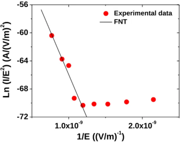
Figure 9. FNT plot for the 6 nm-thick SiOxNy sample.
Figure 9 represents the FNT plot for the 6 nm-thick SiOxNy sample after fitting the experimental data at high electric field to equation (6). This procedure permits to extract parameters as injection barrier B and contact surface. Accordingly, an energy barrier B of 3.28 eV was found. It is in agreement with values reported in the literature, from 2.25 to 3.34 eV for SiO2 layers [26]. For comparison purposes, the Schottky barrier height (SBH) was calculated in the frame of the metal-induced gap states theory accounting for the charge transfer at the metal-dielectric contact [36, 37]. By applying the Schottky pinning parameter Sp = 0.887, as obtained after considering the extracted from spectroscopic ellipsometry measurements electronic part of the dielectric permittivity (§ 3.1), the SBH for electrons was found 3.87 eV.
1.0x10⁻⁹ 2.0x10⁻⁹ -72 -68 -64 -60 -56 Experimental data FNT Ln (I/E 2 ) (A/(V/m) 2 ) 1/E ((V/m)-1)
18
However, the achieved correlation coefficient of the FNT fit is poor, of only 0.92. It leads to a quite high error interval for the contact surface, ranging from 2.4 × 10⁴ nm² to 3.7 × 10⁷ nm², when taking into account the standard deviation of the intercept. Considering the effective surface as Seff = Rc2, the corresponding collection surface ranges from 0.5 × Seff to 760 × Seff.
Neither of the above presented approaches is really convincing in our case. Indeed, the effective contact surface seems to be an adjustment parameter whose physical significance is not straightforward. Considering only mechanical contact is a limitation because it does not take into account the possibility to collect charges by “proximity”, that is to say through air by the curvature of the AFM-tip. Such situation was already demonstrated. Dielectric layers can be charged in “tip-to-sample” space mode, i.e. charges are injected without contact between the tip and the dielectric surface over a distance of around 50 nm [45, 46]. However, the charge collection efficiency strongly depends on the distance to contact point. The latter is in agreement with the presented experimental results.
- Thin dielectric layers (15 nm < d < 150 nm)
To analyze the results for thin SiOxNy-layers (15 nm < d < 150 nm), the current measured in a classical MIM configuration is completed by the C-AFM results. The MIM measurements were performed under controlled atmosphere. The potential Vdc was applied by steps and the current was measured for 1000 s on a 116.8 nm thick SiOxNy layer. The C-AFM measurements were performed on the 50 nm-thick SiOxNy-layer and the current density was obtained after dividing the measured current by an effective contact area (Seff). The upper electrode (probe), is represented by a disk with radius equal to the curvature radius of the tip (Rc = 125 nm). To test the reliability of the procedure and to account for the uncertainty in the effective collection area, the estimation of the current density is completed in the hypothesis of a collection surface 10 and 100 times larger than the Seff. The obtained results are presented in figure 10. Comparison between C-AFM and classical MIM configuration is tough, as applied electric field in the two cases are very different; homogeneous versus inhomogeneous one, with strongly pronounced strengthening at the AFM tip. However, the measured current densities seem consistent with transport mechanisms described by an ohmic behavior at low field, a threshold field of 108V/m which is represented by a change in slope in the log-log diagram, and a high field region where the C-AFM points appear rational with the overall. However, measurements for electric fields in-between these two extremities must be performed to complete and confirm the described trend. Even though the overall picture seems consistent, taking into account of different Seff raises the problem of the effective contact surface between the AFM-tip and the sample. The
19
contact surface can then be used as an adjustable parameter for each experiment. Indeed, studies reported in the literature show that for C-AFM measurements, the contact surfaces should be taken several order greater than the presumed one, a disk with a radius equal to the AFM-tip curvature radius [27-29].
Figure 10. Current density variation for low and high electric fields: I) classical MIM measurements on 116.8 nm thick layer, II) C-AFM measurements on 50 nm thick layer.
Despite the simplicity of the above presented approach, the obtained results underline that a quantitative interpretation of the C-AFM measurements of inorganic thin dielectric layers requires assessment of the collecting surface and consideration of the current density heterogeneity. The same outcome was reached in the case of organic semiconductors [41]. Present results suggest further complexity brought by charge trapping near the AFM tip. The electric field near the tip is obviously modified by the stored charge, by amounts of the order of the applied field by considering the electrostatic modelling made with 2D or 3D charge clouds. Because of these charge trapping effects, injected charges can flow radially over reasonable distance before being collected in the bulk. It means that the apparent collecting surface would have a dynamic character in addition to the uncertainty about its extension.
3.6. Charge dissipation after injection: time evolution for ultrathin and thin SiOxNy-layers We finally consider how the potential profiles evolve in time after charge storage to approach charge dissipation processes. Figure 11 represents the evolution of the potential profile, recorded at different times after injection. Again the ultrathin and thin SiOxNy-layers behave differently. For the ultrathin SiOxNy-layers the surface potential baseline at the end of the injection process is at higher level compared to the surface potential before the charging step. Then a rapid decrease of the reference baseline of the surface potential is observed in time, as shown for the
106 107 108 109 1010 10-9 10-7 10-5 10-3 10-1 101 MIM C-AFM: Seff C-AFM: Seff X10 C-AFM: Seff X100 Curr ent den sity (A/m 2 ) Electric field (V/m) Tuna SiOxNy VDC 50 nm 250 nm AFM Tip VDC pA SiOxNy VDC 116.8 nm 10 mm MIM I II
20
11 nm-thick SiOxNy-layer (figure 11(a)). The surface potential baseline reaches a level close to the initial one, i.e. that the surface potential before charge injection, after 500 s.
The thin dielectric layers are characterized by no modifications of the reference surface potential at the end of the injection with respect to the values before injection. The reference surface potential remains at the same level after injection too, whereas a decrease of the surface potential maximum of the profile occurs, as given for the 31 nm-thick SiOxNy-layer (figure 11(b)).
Figure 11. Evolution of potential profiles with time after injection for (a) ultrathin (11 nm-thick SiOxNy) and (b) thin (31 nm-thick SiOxNy) dielectric layers (injection at V0 = +12 V during 4 min).
A way to better understand these phenomena is to follow the evolution of the surface potential profile baseline as function of time after injection for different layer thicknesses, as shown in figure 12(a). The results confirm the strong modification of the surface potential profile baseline occurring during the charging step, followed by recovery of the initial level for ultrathin layers (the 11 nm-thick SiOxNy on figure 12(a)) due to charge relaxation on Au-electrode. The observed phenomenon for ultrathin layers is actually attributed to charges collection in the buried Au-electrode which is at floating potential during the injection step (as shown in insert of figure 12(a)). Increasing the SiOxNy-layer thickness leads to disappearance of this effect, as confirmed for thin SiOxNy-layers (the 31 nm-thick SiOxNy on figure 12(a)). It means that for thin SiOxNy -layers (15 nm < d < 150 nm) the injected charges do not reach the Au-floating electrode. They are trapped in the dielectric layer close to the contact area. The recorded surface potential profile baseline repeats the one before charge injection, and remains the same during the charge injection step.
These results actually provide information about the charges penetration depth. Indeed, the penetration depth is one of the key parameters to know aiming at extraction of the charges
1 2 3 4 5 0.0 0.2 0.4 0.6 0.8 1.0 Po tential (V) Position (µm) d = 11nm 40s 200s 500s 960s 1270s (a) 1 2 3 4 5 0.0 0.5 1.0 1.5 2.0 Po tential (V) Position (µm) d = 31 nm 40s 200s 600s 980s 1270s (b)
21
density from surface potential measurement [40]. According to the obtained results on the reference surface potential, one can conclude that the charge penetration depth is limited to the thickness of ultrathin dielectric layers (d < 15 nm), thus confirming the assumption made in Section 3.4 for charge penetration depth of 10 nm. The invariance of the reference surface potential for thin layers (15 nm < d < 150 nm) validates the hypothesis of in-depth charge spreading independent from the layer thickness.
Figure 12. (a) Reference surface potential evolution in time after charge injection for ultrathin and thin SiOxNy films (11 nm-thick and 31 nm-thick SiOxNy films), (b) Evolution in time after charge injection of the FWHM and the surface potential profile normalized area, with respect to its initial value, for different film thicknesses. The same charge injection conditions are used in each case: 2 min at V0 = + 5 V.
As far as the time evolution of the other characteristics of the surface potential profile after charge injection, one can observe the same trends for the FWHM and the normalized area with respect to its initial values (figure 12(b)). Regardless the SiOxNy-layer thickness the FWHM of the surface potential profile remains constant in time and the normalized area decreases with the same linear dynamic meaning that the dielectric film thickness does not affect the dissipation behavior of the injected electrical charges. Even for the ultrathin SiOxNy-layers (the 11 nm-thick SiOxNy on figure 12(b)) the trapped charges remain stable. The same charge dissipation behavior determines decay mechanisms being function of the material properties only and not of the layer geometrical aspect; ultrathin or thin SiOxNy-layers. The observed linearly decaying area and constant FWHM of the surface potential after charge injection confirm a charge dissipation mechanism preferentially occurring in the volume of the dielectric layer.
4. Conclusion
The influence of the thickness of thin plasma deposited silicon oxynitride SiOxNy layers on the charge injection mechanisms was investigated in KPFM mode at nanoscale for different applied
0 100 200 300 400 0.0 0.2 0.4 0.6 Po tential (V) Time (s) 11 nm 31 nm (a) 0 300 600 900 1200 1500 0.5 0.6 0.7 0.8 0.9 1.0 1.1 N orm al ized area Time (s) Area 11 nm 31 nm 130 nm 0.0 0.2 0.4 0.6 0.8 1.0 FWHM 11 nm 31 nm 130 nm FWH M (µm ) (b)
22
DC-voltages and injection times. The SiOxNy layers are structurally identical for all thicknesses. The SiOxNy layers are well structured, optically transparent, and having refractive index n = 1.45, equal to the one of silica. Analysis of the recorded surface potential profiles, after performed charge injection, shows distinguished behavior for ultrathin (d < 15 nm) and thin (15 nm < d < 150 nm) dielectric layers. The same is observed for both increased bias voltage and increased injection time. To explain the observed trends a 2D-axisymetric electrostatic model is developed on FEM basis. The FEM modelling emphasizes that during the charge injection step the electric field in the dielectric layer is divergent and strongly enhanced close to the injection point. This enhancement is less pronounced for the ultra-thin dielectric layers for which the dielectric thickness becomes comparable to the curvature radius of the AFM tip. The electric field decreases exponentially in the dielectric layer. The radial electric field component is strong, giving rise to charge spreading in radial direction. The electric field at the contact point determines the amount of injected charges in the dielectric layer. The injected charges are localized close to the injection point. Their penetration depth in the oxynitride dielectric layer in the order of 10 nm. Current versus voltage curves were obtained locally in C-AFM mode. An injection barrier of 3.28 eV has been extracted from FNT plots. Again the ultra-thin and the thin SiOxNy layers behave differently, with mixed behavior for the dielectric layer with thickness in the transition between the two groups. The fast increase in current at high field could be related to Fowler-Nordheim effect. However, incertitude about effective collection surface in C-AFM, configuration of divergent field and probable space charge induced modification of the local field make quantitative assessment tricky. The collection surface seems to have a dynamic character in addition to the uncertainty about its extension. Analysis of charge dissipation in the dielectric layers confirms the second hypothesis for bell-shape distribution of the amount of injected charges in both axial and radial directions and the considered in the model charge penetration depth. Further work will be directed to edge effects induced by the discontinuity of the metal electrode and to analyses of energetics of injected charges, and description of charge trapping and transport in these silica-like SiOxNy layers.
Acknowledgments
This work has been supported by Région Midi-Pyrénées under contract Reference 10051265 and by the program IDEX Actions Thématiques Stratégiques – ATS 2015 of the Université de Toulouse under project SEPHIR (2016-066-CIF-D-DRVD).
23
References
[1] Rao R A, Steimle R F, Sadd M, Swift C T, Hradsky B and Straub S 2004 Silicon nanocrystal based memory devices for NVM and DRAM applications Solid-State Electron. 48, 1463 [2] Perret-Tran-Van S, Makasheva K, Despax B, Bonafos C, Coulon P E and Paillard V 2010
Controlled fabrication of Si-nanocrystals embedded in thin SiON layers by PPECVD followed by oxidizing annealing Nanotechnology 21, 28560
[3] Witvrouw A, Tilmans H A C and De Wolf I 2004 Materials issues in the processing, the operation and the reliability of MEMS Microelectronic Engineering 76, 245–257
[4] http://www.esda.org/
[5] Rezende C A, Gouveia R F, da Silva M A and Galembeck F 2009 Detection of charge distribution in insulator surfaces J. Phys.: Condens. Matter 21, 263002
[6] Lamhamdi M, Pons P, Zaghloul U, Boudou L, Coccetti F, Guastavino J, Segui Y, Papaioannou G and Plana R 2008 Voltage and temperature effect on dielectric charging for RF-MEMS capacitive switches reliability investigation Microelectronics Reliability 48, 1248
[7] Zhang W M, Meng G and Chen D 2007 Stability, nonlinearity and reliability of electrostatically actuated MEMS devices Sensors 7, 760
[8] Teyssedre G, Villeneuve C, Pons P, Boudou L, Makasheva K and Despax B 2012 Challenges in probing space charge at sub-micrometer scale Annual Report IEEE
Conference on Electrical Insulation and Dielectric Phenomena (CEIDP) 234
[9] Hamidouche L, Geron E and Hole S 2017 Very high spatial resolution space charge measurement using electro-acoustic reflectometry (EAR) IEEE Electr. Insul. Mag. 33-5, 9.
[10] Arita Y, Shiratori S and Ikezaki K 2003 A method for detection and visualization of charge trapping sites in amorphous parts in crystalline polymers J. Electrostatics 57 263
[11] Stern J E, Terris B D, Mamin H J and Rugar D 1988 Exposition and imaging of localized charge on insulator surfaces using force microscope Appl. Phys. Lett. 53, 2717
[12] Marchi F, Dianoux R, Smilde H J H, Mur P, Comin F and Chevrier J 2008 Characterization of trapped electric charge carriers behavior at nanometer scale by electrostatic force microscopy Journal of Electrostatics 66, 538
[13] Lambert J, de Loubens G, Guthmann C and Saint-Jean M 2002 Dispersive charge transport along the surface of an insulating layer observed by electrostatic force microscopy Phys.
24
[14] Tzeng S-D and Gwo S 2006 Charge trapping properties at silicon nitride/silicon oxide interface studied by variable-temperature electrostatic force microscopy J. Appl. Phys. 100, 023711
[15] Morita S, Uchihashi T, Okamoto K, Abe M and Sugawara Y 2005 Microscale contact charging on silicon oxide Characterization, Nanofabrication and Device Application of
Functional Materials 186, 289
[16] Charrier D S H, Kemerink M, Smalbrugge B E, Vries T and Janssen R A J 2008 Real versus measured surface potentials in scanning Kelvin Probe Microscopy ACS Nano 2, 622
[17] Borowik L, Kusiaku K, Theron D and Melin T 2010 Calculating Kelvin force microscopy signals from static force fields Appl. Phys. Lett. 96, 103119
[18] Ishii M. 2010 Static states and dynamic behaviour of charges: observation and control by scanning probe microscopy J. Phys.: Condens. Matter 22, 173001.
[19] Zaghloul U, Bushan B, Pons P, Papaioannou G J, Coccetti F and Plana R 2011 On the influence of environment gases, relative humidity and gas purification on dielectric charging/discharging processes in electrostatically driven MEMS/NEMS devices
Nanotechnology 22, 035705
[20] Zaghloul U, Bushan B, Pons P, Papaioannou G J, Coccetti F and Plana R 2010 A systematic reliability investigation of the dielectric charging process in electrostatically actuated MEMS based on Kelvin Force Microscopy J. Micromech. Microeng. 20, 064016
[21] Ziegler D, Naujoks N and Stemmer A 2008 Feed-forward compensation of surface potential in atomic force microscopy Review of Sci. Instrum. 79, 063704
[22] Lanza, M. 2017 Conductive Atomic Force Microscopy: Applications in Nanomaterials
Wiley-VCH Verlag: Weinheim, Germany
[23] Foissac R, Blonkowski S, Kogelschatz M, and Delcroix P 2014 A relationship between statistical time to breakdown distributions and pre-breakdown negative differential resistance at nanometric scale J. Appl. Phys.116, 024505
[24] Seko A, Watanabe Y, Kondo H, Sakai A, Zaima S and Yasuda Y 2004 Behavior of Local current leakage in stressed gate SiO2 films analyzed by Conductive Atomic Force Microscopy Jpn J. Appl.Phys. 43, 4683
[25] Frammelsberger W, Benstetter G, Kiely J and Stamp R 2007 C-AFM-based thickness determination of thin and ultra-thin SiO2 films by use of different conductive-coated probe tips Appl. Surf. Sci. 253, 3615
25
[26] Frammelsberger W, Benstetter G, Stamp R, Kiely J and Schweinboeck T 2005 Simplified tunnelling current calculation for MOS structures with ultra-thin oxides for conductive atomic force microscopy investigations Materials Science and Engineering B 116, 168 [27] Olbrich A, Ebersberger N and Boit C 2001 Nanoscale electrical characterization of thin
oxides with conductive atomic force microscopy 36th annual IEEE IRPS, 2934
[28] Porti M, Nafra M, Aymerich X, Olbrich A and Ebersberger B 2001 Nanometer-scale electrical characterization of stressed ultra-thin SiO2 film using conducting atomic force microscopy Appl. Phys. Lett. 78, 4181
[29] Olbrich A, Ebersberger B, Boit C, Vancea J and Hoffmann H 1999 A new AFM-based tool for testing dielectric quality and reliability on a nanometer scale Microelectronics
Reliab. 39, 941
[30] Makasheva K, Despax B, Boudou L and Teyssedre G 2012 Dielectric layers for RF-MEMS switches: design and study of appropriate structures preventing electrostatic charging
IEEE Trans. Dielectrics and Electrical Insulation 19, 1195
[31] Villeneuve-Faure C, Makasheva K, Bonafos C, Despax B, Boudou L, Pons P and Teyssedre G 2013 Kelvin force microscopy characterization of charging effect in thin a-SiOxNy:H layers deposited in pulsed plasma enhanced chemical vapor deposition process by tuning the silicon environment J. Appl. Phys. 113, 204102
[32] WinElli Software by SOPRA S.A. Version 3.04 1999
[33] Forouhi A R and Bloomer I 1986 I Optical dispersion relations for amorphous semiconductors and amorphous dielectrics Phys. Rev. B 34, 7018–7026
[34] Wang Y and Irene E A 2000 Consistent refractive index parameters for ultrathin SiO2 films
J. Vac. Sci. Technol. B, 18, 279-282
[35] Radouane K, Date L, Yousfi M, Despax B and Caquineau H 2000 RF discharge modelling in a N2O/SiH4 mixture for SiO2 deposition and comparison with experiment J. Phys. D:
Appl. Phys. 33 1332–1341
[36] Robertson J and Falabretti B 2006 Band offsets of high K gate oxides on III-V semiconductors J Appl. Phys., 100, 014111
[37] Villeneuve-Faure C, Makasheva K, Boudou L, and Teyssedre G 2016 Charge injection in thin dielectric layers by atomic force microscopy: influence of geometry and material work function of the AFM tip on the injection process Nanotechnology 27, 245702 [38] Boularas A, Baudoin F, Villeneuve-Faure C, Clain S and Teyssedre G 2014
Multi-dimensional modelling of electrostatic force distance curve over dielectric surface: Influence of tip geometry and correlation with experiment J. Appl. Phys. 116, 084106
26
[39] Sacha G M, Cardellach M, Segura J J, Moser J, Bachtold A, Fraxedas J and Verdaguer A 2009 Influence of the macroscopic shape of the tip on the contrast in scanning polarization force microscopy images Nanotechnology 20, 285704
[40] Palleau E, Ressier L, Borowik Ł and Mélin T 2010 Numerical simulations for a quantitative analysis of AFM electrostatic nanopatterning on PMMA by Kelvin force microscopy Nanotechnology 21, 225706
[41] Reid O G, Munechika K and Ginger D S 2008 Space charge limited current measurements on conjugated polymer films using Conductive Atomic Force Microscopy NanoLetters 8, 1602
[42] Hebert K J, Zafar S, Irene E A, Kuehn R, McCarthy T E and Demirlioglu E K 1996 Measurement of the refractive index of thin SiO2 films using tunneling current, oscillations and ellipsometry Appl. Phys. Lett. 68, 266
[43] Ruskell TG, Workman R, Chen D, Sarid D, Dalh A and Gilbert S 1996 High-resolution Fowler-Nordheim field emission map of thin silicon oxide layers Appl. Phys. Lett. 68, 93 [44] Celano U, Hantschel T, Giammaria G, Chandra Chintala R, Conard T, Bender H and Vandervorst W 2015 Evaluation of the electrical contact area in contact-mode scanning probe microscopy J. Appl. Phys. 117, 214305
[45] Ressier L and Le Nader V 2008 Electrostatic nanopatterning of PMMA by AFM charge writing for directed nano-assembly Nanotechnology 19, 135301
[46] Makasheva K, Villeneuve-Faure C, Laurent C, Despax B, Boudou L and Teyssedre G 2015 Dielectric charging by AFM in tip-to-sample space mode: overview and challenges in revealing the appropriate mechanisms Nanotechnology 26, 295704