HAL Id: tel-01053729
https://tel.archives-ouvertes.fr/tel-01053729
Submitted on 1 Aug 2014
HAL is a multi-disciplinary open access
archive for the deposit and dissemination of sci-entific research documents, whether they are pub-lished or not. The documents may come from teaching and research institutions in France or abroad, or from public or private research centers.
L’archive ouverte pluridisciplinaire HAL, est destinée au dépôt et à la diffusion de documents scientifiques de niveau recherche, publiés ou non, émanant des établissements d’enseignement et de recherche français ou étrangers, des laboratoires publics ou privés.
To cite this version:
Eldar Zianbetov. Distributed clocking for synchronous SoCs. Micro and nanotechnolo-gies/Microelectronics. Université Pierre et Marie Curie - Paris VI, 2013. English. �tel-01053729�
TH `
ESE DE DOCTORAT DE
l’UNIVERSIT ´
E PIERRE ET MARIE CURIE
´
Ecole Doctorale Informatique, T´el´ecommunications et ´
Electronique
(EDITE)
Pr´esent´ee par :
Eldar ZIANBETOV
Pour obtenir le grade de :
DOCTEUR de l’UNIVERSIT ´
E PIERRE ET MARIE CURIE
Sujet de la th`ese :
HORLOGERIE DISTRIBU ´
EE POUR LES SOCs SYNCHRONES
Pr´esent´ee le : 25.03.2013 Le jury est compos´e de :
M. Jean-Baptiste BEGUERET IMS Bordeaux Rapporteur
M. David NAIRN Universit´e de Waterloo Rapporteur
M. Jean-Pierre SCHOELLKOPF SiLiCieL Rapporteur
M. Bernard COURTOIS CNRS Examinateur
M. Alain GREINER UPMC, LIP6 Examinateur
M. Valeriy SITNIKOV Odessa State Polytechnic University Examinateur
M. Franc¸ois ANCEAU CNAM Directeur de Th`ese
M. Dimitri GALAYKO UPMC, LIP6 Co-directeur de Th`ese
M. ´Eric COLINET CEA-LETI, Minatec Invit´e
DOCTORAL DISSERTATION
PIERRE AND MARIE CURIE UNIVERSITY
Doctoral School of Informatics, Telecommunications and Electronics
(EDITE)
Presented by:
Eldar ZIANBETOV
To obtain the degree of :
DOCTOR OF PHILOSOPHY AT UNIVERSITY OF PIERRE AND
MARIE CURIE
Thesis title :
DISTRIBUTED CLOCKING FOR SYNCHRONOUS SOC
Presented on : 25.03.2013 Members of jury :
M. Jean-Baptiste BEGUERET IMS Bordeaux Reviewer
M. David NAIRN University of Waterloo Reviewer
M. Jean-Pierre SCHOELLKOPF SiLiCieL Reviewer
M. Bernard COURTOIS CNRS Examinator
M. Alain GREINER UPMC, LIP6 Examinator
M. Valeriy SITNIKOV Odessa State Polytechnic University Examinator
M. Franc¸ois ANCEAU CNAM Supervisor
M. Dimitri GALAYKO UPMC, LIP6 Co-Supervisor
M. ´Eric COLINET CEA-LETI, Minatec Invited
Abstract
This dissertation addresses the problem of global synchronization of complex SoC in the context of deeply submicron CMOS technologies.
Nowadays, to circumvent the difficulties associated with conventional clock distribution techniques (e.g. tree, mesh) in synchronous systems, the designers wishing to go on with the Globally Synchronous paradigm are turning toward clocking techniques breaking away from conventional approaches (e.g. distributed oscillators, stationary waves, coupled oscillators, programmable delays). This study is situated on this research axis.
In this research we studied and elaborated a global distributed clocking system for a highly reliable synchronous circuit. This clocking scheme is based on a network of oscilla-tors coupled in phase. Inside each synchronous clocking domain, there is one oscillator that generates the local clock. To synchronize the oscillators (i.e. domains), each one of them is controlled by an All-Digital Phase Locked Loop (ADPLL), realizing a phase coupling between the oscillators of neighboring zones.
During this research we have developed the specifications and selected an architecture of the network. A theoretical model of the system has been established in a collaboration with CEA-LETI and Sup´elec laboratories in the framework of ANR HODISS project. We have analyzed the behavior of the system in simulations on different abstraction levels, investi-gated the stability conditions of its synchronous operation.
An All-Digital Phase Locked Loop (ADPLL) has been proposed for the role of an el-ementary node of distributed clocking network. The use of ADPLL permits to circumvent difficulties of implementation, which are usually associated with analog PLL. We have de-signed the main blocks of the ADPLL: a Digitally-Controlled Oscillator (DCO), a Phase-Frequency Detector (PFD) and an error processing block. A cell-based design technique has been adapted for the design of DCO layout. This technique significantly reduced the com-plexity of the oscillator’s implementation. The remaining blocks have been designed in a common digital design flow.
In order to reduce the risks associated with silicon implementation, the system has been validated in a FPGA prototyping platform. The results of the measurements showed that clocking network behaves as predicted by the theory and simulations.
Two prototype circuits have been designed, implemented and tested in a 65 nm STMi-croelectronics CMOS technology. The first one is a proof of concept of a designed highly linear and monotonous DCO. The measured parameters of oscillator showed the compli-ance with specifications. The measured performcompli-ance demonstrated the <15 ps rms jitter, while consuming 6.2 mW/GHz with 1.1 V supply voltage. The tuning range of the oscil-lator is 999-2480 MHz under 10 bit resolution. The second chip is a 4×4 node clocking network which consists of 16 distributed ADPLLs. Each of them employs a designed earlier DCO, PFD and error processing block. The experiments showed that proposed technique of distributed clock generation is feasible in a real CMOS chip environment. The measured per-formance demonstrated the timing error between neighbor oscillators less than 60 ps, while power consumption is 98.47 mW/GHz.
loop, digitally-controlled oscillator, bang-bang detector, time-to-digital converter
Thesis Supervisor: Franc¸ois ANCEAU, Professor at Conservatoire national des arts et m´etiers
Thesis Co-Supervisor: Dimitri GALAYKO, Associate Professor at Pierre and Marie Curie University (Paris VI)
The meaning of this degree is that the recipient of instruction is examined for the last time in his life, and is pronounced completely full.
Acknowledgements
With a great sincerity I wish to express my deep gratitude to all those who helped me to carry out my doctoral work. I have been surrounded by family, friends, project partners, labmates, colleagues and professors who have provided support and aid during this research. This thesis would not have been possible without the guidance, patience and generosity of my supervisor Dimitry Galayko. I am grateful to him for giving me the opportunity to do the research in such a marvelous city as Paris. I would like to deeply thank for his continuous support, encouragement and help. I am also very grateful to my supervisor Franc¸ois Anceau for his ambitions and inspiring enthusiasm. During these years he has been a source of ideas, knowledge and motivation for me. It has been a honor working and collaborating with them. I want to express my thanks to our collaborators ´Eric Colinet, J´erˆome Juillard and Sylvain F´eruglio. A special thanks to Mehdi Terosiet, Anton Korniienko and Jean-Michel Akr´e for precious discussions and of course for their time spent on explaining me things out of my competence.
I would like also to thank Valeriy Sitnikov for giving me an initial burst of enthusiasm on this encouraging and challenging way of research.
A big thank for all my labmates as well. They created a warm and friendly atmosphere in our team and the excellent research environment in the CIAN group. A special thank to Diomadson Belfort, who helped me a lot with CAD tools, simulations, design of layout and showed many special ”magic” tricks – they saved countless hours of my efforts. Another special thank to Mohammad Javidan for his valuable help in carrying out the design of the second chip.
The specialists in CEA-LETI and CMP center helped to make the tape-out processes as easy as it was possible. In particular, the hours spent on verifying my designs with Kholdoun Torki and Olivier Billoint was very useful.
I thank my wife, Maria, for moral support and encouragement in my private life all these years. Thank you for organizing all our vacations.
Finally, my thanks go to all those who participated more or less indirectly to the success of my thesis.
Contents
1 Introduction 1
1.1 Area of focus . . . 1
1.1.1 Clocking in large digital circuits . . . 2
1.1.2 Clock error issues . . . 4
1.2 State of the art: synchronous clocking in modern SoC . . . 6
1.2.1 Conventional clock trees . . . 6
1.2.2 Optical distribution technique . . . 8
1.2.3 Multioscillator architectures . . . 9
1.2.4 Synchronous clocking architectures: conclusion . . . 12
1.3 Thesis outline and contribution . . . 14
2 Network of distributed ADPLLs 15 2.1 Introduction . . . 15
2.2 Proposed clocking architecture . . . 16
2.2.1 Network of coupled PLLs . . . 16
2.2.2 Digital phase synthesis . . . 18
2.2.3 Blocks of the ADPLL network . . . 19
2.2.4 Specification of clocking network parameters . . . 22
2.3 Multiplicity of synchronisation modes . . . 25
2.3.1 Definition of the problem . . . 25
2.3.2 Synchronization mode selection . . . 26
2.4 Stability of the PLL networks . . . 29
2.5 Modeling of the clocking network . . . 30
2.5.1 The model of the phase comparator . . . 30
2.5.2 Loop filter . . . 31
2.5.3 DCO. . . 31
2.5.4 Simulation of ADPLL . . . 31
2.5.5 Simulation of network . . . 32
2.6 Conclusion . . . 38
3 Digitally controlled oscillator design 39 3.1 Introduction . . . 39
3.2 Digital frequency tuning in ring oscillators . . . 42 xiii
3.2.1 Capacitive tuning . . . 43
3.2.2 Current/Voltage tuning . . . 44
3.2.3 Current tuning with width modulation technique . . . 44
3.2.4 Frequency tuning in 2D array oscillator . . . 46
3.2.5 The choice of the coding . . . 48
3.3 DCO architecture . . . 52
3.3.1 Oscillator topology . . . 52
3.3.2 Control algorithm . . . 53
3.4 Sizing of the DCO core and tuning cells . . . 57
3.5 VHDL modeling of the oscillator . . . 58
3.5.1 Precise modeling of the real code-frequency characteristic . . . 58
3.5.2 Synthesis of the DCO output frequency in the precise VHDL model 59 3.6 DCO layout desing I: the DCO floorplan . . . 61
3.6.1 Cell based design . . . 61
3.6.2 Power planning . . . 62
3.6.3 Signal flow oriented layout . . . 63
3.6.4 Guard rings . . . 64
3.6.5 General DCO floorplan . . . 64
3.7 DCO layout design II: cell design. . . 65
3.7.1 Main inverters . . . 65
3.7.2 Feedback wire and decoupling capacitors . . . 66
3.7.3 Tuning inverters . . . 67
3.7.4 DCO output interface . . . 71
3.7.5 A, B and C bus generator . . . 72
3.7.6 DCO chip . . . 73
3.8 DCO chip test . . . 76
3.8.1 Impact of the supply variations . . . 76
3.8.2 Chip-to-chip variations . . . 76
3.8.3 Power consumption . . . 77
3.8.4 Linearity . . . 78
3.8.5 Jitter characteristics . . . 78
3.9 Conclusion . . . 80
4 Digital blocks of the ADPLL 81 4.1 Introduction . . . 81
4.2 Digital phase/frequency error measurement . . . 82
4.2.1 Digital versus analog phase comparators . . . 82
4.2.2 Phase comparators versus phase-frequency detectors . . . 83
4.2.3 The digital PFD architecture . . . 85
4.2.4 Metastability problem. . . 87
4.3 Implementation of digital PFD . . . 89
Contents xv
4.3.2 Time-to-digital converter . . . 94
4.3.3 Implementation of PFD . . . 96
4.4 Digital loop control of ADPLL network node . . . 99
4.4.1 Error combining block . . . 99
4.4.2 PI filter . . . 100
4.4.3 Implementation . . . 101
4.4.4 ADPLL simulation results . . . 101
4.5 Node programming mechanism . . . 105
4.6 Conclusion . . . 107
5 Clock network implementation 109 5.1 Introduction . . . 109
5.2 FPGA prototyping . . . 111
5.2.1 Synthesizable DCO . . . 112
5.2.2 FPGA based TDC. . . 114
5.2.3 Experimental results . . . 115
5.2.4 FPGA prototyping: conclusion . . . 120
5.3 Silicon implementation of the clock network . . . 122
5.3.1 Floorplan of the test chip . . . 122
5.3.2 Design for test. . . 124
5.3.3 Test chip layout . . . 127
5.4 Measurement results . . . 130
5.4.1 Initial frequencies of DCOs . . . 130
5.4.2 Supply voltage sensivity . . . 131
5.4.3 Power consumption . . . 131
5.4.4 Bidirectional configuration . . . 132
5.4.5 Unidirectional configuration . . . 133
5.4.6 Corner to corner timing errors . . . 135
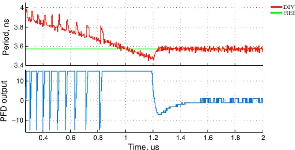
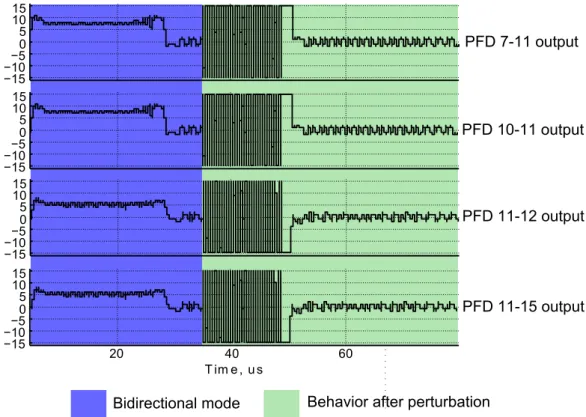
5.4.7 Study of mode-locking phenomenon . . . 136
5.4.8 Coefficient variation . . . 137
5.5 Conclusion . . . 141
6 Conclusion and Perspectives 143 6.1 Thesis summary and conclusions . . . 143
6.2 Future work . . . 145
Appendices 147
A VHDL models of the ADPLL blocks 149
B Phase error sign detection theorem proof 165
D DCO test chip characterization flow 175
E FPGA prototyping of the clocking network 179
F VLSI implementation of the network 185
G Clocking network test chip characterization flow 187
List of Figures
1.1 Amount of transistors in microprocessors and SoC. . . 2
1.2 Frequency of the Intel microprocessors . . . 2
1.3 Clock domains in a SoC. . . 3
1.4 Flow of the data in clocked system and its timing digram . . . 4
1.5 Definition of the skew and jitter. . . 5
1.6 Examples of conventional clock distribution tree structures . . . 6
1.7 Typical mesh clock network . . . 7
1.8 Centralized skew compensation technique . . . 8
1.9 Example of decentralized skew compensation technique . . . 9
1.10 An optical clock distribution network. . . 9
1.11 Network of oscillators coupled by voltage . . . 10
1.12 Standing-wave clocking principle. . . 11
1.13 Distributed PLL . . . 11
1.14 Network node . . . 12
1.15 16-node distributed clocking network. . . 12
2.1 Basic idea of multioscillator clocking approach . . . 16
2.2 Topology of the proposed clock network and architecture of the network node . 17 2.3 Phase coupling between two oscillators . . . 17
2.4 Block diagram of the ADPLL. . . 18
2.5 Block diagram of the PI filter . . . 21
2.6 Transfer function of the digital phase comparator . . . 22
2.7 Definition of two main design constraints for the clocking network . . . 23
2.8 Frequency tuning limits consideration . . . 24
2.9 Cyclic nature of the conventional analog linear phase comparator . . . 25
2.10 Illustration of the mode-locking phenomenon in a 2×2 mesh network . . . 26
2.11 Transfer function of the phase comparator to avoid undesirable states . . . 26
2.12 Propagation of the phase information in unidirectional network . . . 27
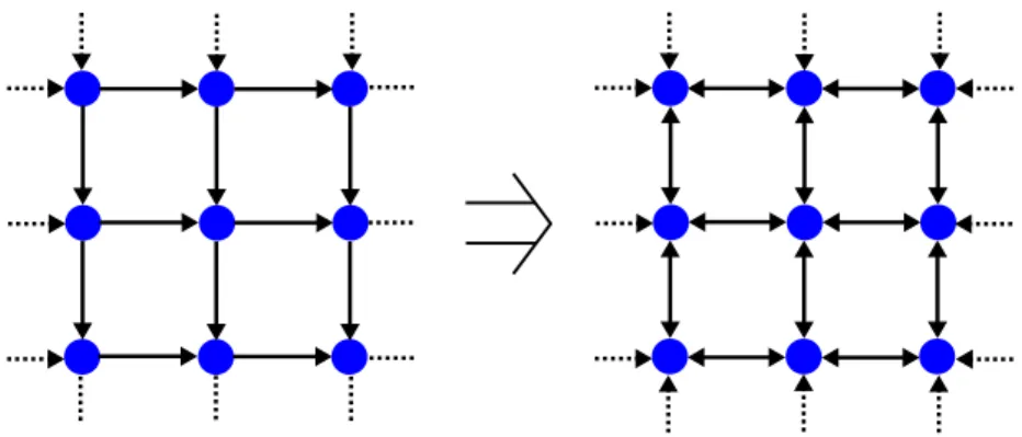
2.13 Dynamic reconfiguration of the network from uni- to bidirectional . . . 28
2.14 Representation of the PLL network for stability study in [59] . . . 29
2.15 Block diagram of the modeled phase comparator. . . 30
2.16 Principle of the VHDL implementation of digital period-controlled oscillator . 31 2.17 Simulation of the developed VHDL model of ADPLL . . . 32
2.18 Simulated 16-node clocking network . . . 33 xvii
2.19 Simulation of the developed VHDL model of 16-node network . . . 35
2.20 Errors of the PFDs connected to the node 11 in first experiment . . . 35
2.21 Simulation of the developed VHDL model of 16-node network . . . 36
2.22 Simulation results of dynamicly reconfigurable network . . . 37
3.1 Representation of DCO as a combination of DAC and VCO . . . 40
3.2 Inverter-based ring oscillator . . . 42
3.3 CMOS inverter with parasitic components . . . 43
3.4 Charge and discharge of parasitic capacitance in CMOS inverter . . . 43
3.5 Capacitive tuning in a ring oscillator . . . 44
3.6 Current tuning in a ring oscillator. . . 44
3.7 Current tuning technique with direct digital control . . . 45
3.8 Digital delay control principle . . . 46
3.9 Frequency tuning in 2D array oscillator . . . 47
3.10 Thermometer current coding . . . 49
3.11 Binary current coding . . . 50
3.12 Core of the proposed oscillator . . . 52
3.13 Virtual extension of number of stages . . . 54
3.14 Oscillator control grid . . . 55
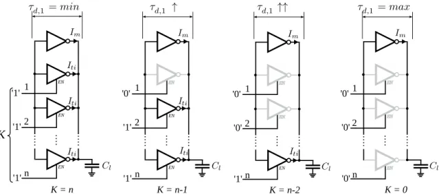
3.15 Approximation of the code-frequency characteristic in VHDL model of DCO . 58 3.16 Structure of the implemented VHDL model . . . 59
3.17 Period-controlled oscillator with jitter . . . 59
3.18 Simulation of the DCO behavioral model . . . 60
3.19 Interdigitated multi-finger power routing . . . 61
3.20 Cell layout template . . . 62
3.21 Supply decoupling polysilicon CMOS capacitor . . . 63
3.22 Signal flow driven placement of the tuning cells in DCO . . . 64
3.23 Guard rings around oscillator core . . . 64
3.24 Floorplan of the designed oscillator. . . 65
3.25 Schematic of a main inverter of oscillator . . . 66
3.26 Layout of the feedback line/decoupling capacitance service cell . . . 67
3.27 Feedback/decoupling capacitor cell in the power distribution network. . . 67
3.28 Single tuning cell layout template . . . 68
3.29 Schematic diagram of the coarse tuning cells. . . 68
3.30 Layout of the coarse tuning cells . . . 69
3.31 Schematic diagram of the additional coarse tuning cells . . . 69
3.32 Additional coarse tuning cells layout . . . 70
3.33 Schematic diagram of the fine tuning cells . . . 70
3.34 Layout of the FTI cell . . . 71
3.35 Improvement of duty cycle by divider . . . 71
3.36 Schematic diagram of the feedback frequency divider . . . 71
List of Figures xix
3.38 Schematic of the A, B and C signal generation circuit . . . 73
3.39 Layout of the B2T decoders. . . 73
3.40 Schematic diagram of the DCO test chip . . . 74
3.41 Microphotograph of the fabricated chip . . . 75
3.42 Measured and simulated output frequency versus input control code for different supply voltages . . . 76
3.43 Measured tuning curves for 7 samples of fabricated circuits . . . 77
3.44 Measured and simulated power consumption versus input control code . . . 77
3.45 Measured differential nonlinearity of the circuit . . . 78
3.46 Measured jitter versus control code . . . 78
4.1 XOR phase comparator . . . 82
4.2 Conventional phase comparator . . . 83
4.3 The phase/frequency detector . . . 84
4.4 Two cases of initial conditions in phase/frequency detector . . . 85
4.5 Detection of the phase error sign variation . . . 85
4.6 Proposed phase/frequency detector for clock network . . . 86
4.7 Principle of operation of proposed PFD . . . 86
4.8 Simplest trigger circuit . . . 87
4.9 Proposed in [67] arbiter circuit . . . 87
4.10 Schematic diagram of the bang-bang phase/frequency detector . . . 89
4.11 Circuit diagram of the reduced flip-flop . . . 91
4.12 Circuit diagram of the metastability filter with RS-trigger . . . 91
4.13 Circuit diagram of the Muller C-element . . . 91
4.14 Delay of the arbiter as a function of timing error . . . 92
4.15 Degradation of the bang-bang loop delay with smaller input errors . . . 93
4.16 Layout of the bang-bang detector . . . 93
4.17 Time-to-digital converter . . . 95
4.18 Block diagram of proposed time-to-digital converter . . . 95
4.19 Simulated transfer function of the designed flash time-to-digital converter . . . 96
4.20 Layout of the TDC employing standard cells . . . 97
4.21 Simulation of the designed multi-bit PFD . . . 98
4.22 Signal flow diagram for proposed PFD . . . 98
4.23 Layout of the proposed PFD . . . 98
4.24 Error signal processing block . . . 99
4.25 Layout of the digital signal processing block . . . 102
4.26 Layout of the test ADPLL . . . 103
4.27 Simulation of the designed ADPLL with proposed oscillator, PFD and signal processing block . . . 104
4.28 Schematic of the programming interface . . . 106
5.1 Structure of the implemented clock network . . . 110
5.2 Repeating discrete ramp function in the DDFS . . . 112
5.3 Schematic diagram of the proposed FPGA implementation of the oscillator . . 113
5.4 Conventional phase detector . . . 115
5.5 Block diagram of the node in a FPGA prototype with observation points . . . . 116
5.6 Local clock signals together with reference. . . 117
5.7 Local clock signals together with reference. . . 118
5.8 Local clock signals around Node 10 together with reference and integer sum of the errors . . . 118
5.9 Local clock signals together with reference. . . 119
5.10 Local clock signals around Node 10 together with reference and integer sum of the errors . . . 119
5.11 Local clock signals together with reference. . . 120
5.12 Local clock signals around Node 10 together with reference and integer sum of the errors . . . 120
5.13 Preliminary floorplan of the test chip . . . 123
5.14 Power supply scheme of the test chip . . . 123
5.15 Simulation of the extracted from layout supply distribution network . . . 124
5.16 The connection sequence of the programmable blocks of the network. . . 125
5.17 Block diagram of the node in a ASIC implementation . . . 126
5.18 Multichannel multiplexer with serial interface for the PFD output commutation 126 5.19 Layout of the test chip of the clock network . . . 128
5.20 Microphotograph of the fabricated clocking network test circuit. . . 129
5.21 Measured initial frequencies of the DCOs . . . 131
5.22 Measured supply voltage sensivity of the DCOs . . . 132
5.23 Measured current consumption of the network . . . 132
5.24 Histogram of the reference clock . . . 133
5.25 Zones of the network for the measurement . . . 133
5.26 Synchronous clocks in the bidirectional configuration . . . 134
5.27 Outputs of the PFDs from the Zone 9 in bidirectional configuration . . . 134
5.28 Outputs of the PFDs from the Zone 9 in unidirectional configuration . . . 135
5.29 Timing error between corner nodes . . . 136
5.30 Configuration of the network for mode-locking study . . . 137
5.31 Misaligned clocks in the mode-locking state . . . 137
5.32 Outputs of the PFDs in the mode-locking state . . . 138
5.33 Transient process in the Node 11 depending on variation of the coefficient Kp and Ki . . . 139
B.1 Sign detection in BB circuit. . . 165
D.1 Schematic of the developed PCB . . . 177
List of Figures xxi
E.1 Functional diagram of Cyclone II DSP Development Board . . . 183
E.2 Top view of Cyclone II DSP Development Board . . . 183
E.3 FPGA prototyping platform . . . 184
F.1 Complete block diagram of the clock network and DFT blocks . . . 186
G.1 Schematic of the developed PCB for network chip testing . . . 189
List of Tables
2.1 Clocking network implementation specification . . . 24
2.2 ADPLL simulation parameters and conditions summary . . . 32
2.3 Clocking network simulation parameters and conditions summary . . . 34
3.1 Dimensions of the transistors in the DCO cells . . . 57
3.2 Layers functionality attribution . . . 63
3.3 DCO chip performance summary . . . 79
4.1 C-element truth table . . . 90
4.2 Simulation parameters and conditions . . . 102
5.1 Parameters of the FPGA and VLSI implementations of the DCO . . . 116
5.2 Clock network test chip measurement conditions . . . 130
5.3 Network test chip measurements summary . . . 140
Chapter 1
Introduction
Contents
1.1 Area of focus . . . 1
1.2 State of the art: synchronous clocking in modern SoC . . . 6
1.3 Thesis outline and contribution . . . 14
1.1
Area of focus
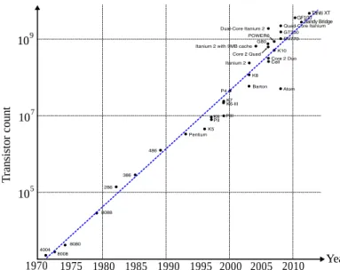
Nowadays, numerous scientific, industrial and multimedia tasks are performed by elec-tronic devices based on Systems-On-Chip (SoC). Over the past decade, SoCs evolved from systems with thousands transistors performing simple information processing toward high-performance multiprocessor systems able to perform billions of operations per second. Till recently, the growth of the SoC performance has been obtained through an intensive strategy: reducing the transistor size, increasing the number of gates per chip (Fig.1.1), increasing the clock frequency. Whereas the chip density increases following the Moore law, the clock frequency evolution has stalled since several years at the level of 500-4000 MHz (Fig. 1.2). Further increase of the processing power of chips is achieved through association of several parallel processing units on chips, and by optimizing their interaction.
The saturation of the clock frequency growth is explained by the difficulties of a global clock distribution over a large chip designed in deeply submicron CMOS technologies, and by a high energy cost of such distribution. Indeed, for gigahertz clock frequencies, a linear increase of the clock frequency∗ implies an exponential increase of the consumed power. This goes against the requirements of low-power autonomous systems which are the domi-nant applications on the nowadays market [50]. For those reasons, the SoC designers limit the clock frequencies to few hundred megahertz, and look toward SoC architectures which do not require a global clock generation: e.g. GALS(Globally Asynchronous Locally Syn-chronous). However, although clockless asynchronous approaches are gaining ground [25],
∗Usually in combination with increase of supply voltage
Figure 1.1: Amount of transistors in microprocessors and SoC of various companies over past 30 years
Figure 1.2: Frequency of the Intel microprocessors over past 30 years
synchronous approach remains the preferred on-chip communication technique, mainly be-cause of the better mastering and prediction of synchronous circuits behavior [21].
This study addresses the problem of global clock generation inside complex and large SoC: e.g. MPSoC (Multi Processor SoC). It is motivated by deficiencies of conventional clock generation approaches such as a clock grid or a tree in the context of deeply submi-cron CMOS technologies. The developed clock generation technique is based on a coupled oscillators network distributed over the chip.
1.1.1
Clocking in large digital circuits
Nowdays, large digital chip are partitioned into local clock areas (domains) [79, 52, 33,
1.1. Area of focus 3
isochronous zone
clock amplifier initial clock
i
(a) functional isochronous zone(b)
h
Figure 1.3: Clock domains in a SoC: (a) isochronous zone and (b) their placement in SoC
Areas (SCA) [30]. Each zone has its own local clock; these zones are small, so the clock distribution inside the zones can be achieved without difficulties by conventional techniques. The size of the zone is determined by the maximal delay that can experience the clock signal while being routed through the zone (cf. Fig.1.3): this delay should be small enough for the constraint-less clock routing. The dimensions of the zone depends on the technology, and the number of gates/latches is approximately 200-300 thousands.
The communication inside the SCAs is synchronous; the communication between the blocks situated in different SCAs can be synchronous or asynchronous. In the first case the chip is GSLS (Globally Synchronous Locally Synchronous), in the latter case the chip is GALS.
In a GSLS system, the local clock oscillators are synchronized in phase. In this way, synchronous communications are possible through the borders of the neighboring SCAs, and the whole SoC can be designed with the conventional methodology of synchronous digital design. The advantages of the synchronous circuits are their reliability, deterministic behavior and high communication rate.
However, the synchronization of local clocks of the SCAs in a large chip is a very diffi-cult task. The global clock signal must be routed over the whole chip surface, whereas the delay matching should be guaranteed with a picosecond resolution: this goal is very chal-lenging, and its power and area cost are prohibitive. To date, mainly conventional clocking techniques like clock tree and grid are used in the commercial circuits. These clock genera-tion and distribugenera-tion architectures are sometimes reinforced by resynchronizagenera-tion blocks, so to compensate the timing errors due to mismatch, temperature and supply drift.
Because of these difficulties, the SoC engineers orient their choice toward GALS archi-tecture which does not require the global clock. In a GALS system, the local SCA clocks are independent, and the communication between the zones is asynchronous. The bisynchronous interfaces guaranteeing the signal integrity during such communication are complex blocks which also reduce the communication speed. Moreover, asynchronous circuits may experi-ence metastability whose probability can be reduced to very small values, but never being eliminated. Finally, asynchronous circuits do not have a deterministic behavior: their relia-bility is more difficult to guarantee at the design stage than for the synchronous circuits.
This work is addressed to the designers developing GSLS circuits: the proposed solution is an alternative to traditional global clock distribution techniques.
1.1.2
Clock error issues
In any synchronous circuit design, the engineers mainly develop the combinatorial networks performing the required functions. These networks are supplied with the cascading registers which synchronize the flow of information among the data propagation paths.
Fig.1.4summarizes the principle of the synchronous communication. The data is set by register Risynchronously with an event of the clock CLKi. After a delay due to
interconnec-tion lines and to the combinatorial logic processing the data, the signal arrives at the input of the register Rf synchronized by the clock CLKf. Ideally, the two clocks must be
iden-tical (synchronous). The processed data should arrive at the input of the register Rf before
the arriving of the next clock event of CLKf. In this way, the whole delay of the data path,
including the delay and setup/hold time of Rf must be less than the clock period.
Data in RegisterR Combinatorialnetwork RegisterR Data out
Data path C-Q IC LOGIC IC SET Data Clock CLK tk CLKi CLKf T >0 T <0 T T T T T f i i t kf k k
Figure 1.4: Flow of the data in clocked system and its timing digram
In practice, the clocks CLKiand CLKf experience a synchronization error : the later can
be seen as difference in the instants of the must-to-be synchronous events of the two clocks: ∆Tk= tki− t
f
k, (1.1)
where tki and tkf are the instants of arriving of kth clock events at the input of each regis-ters. ∆Tk is a discrete random process usually considered as ergodic, and characterized by
the average value called skew and the residual zero-centered random process called jitter (Fig.1.5). In practice jitter is considered as being determined and limited, and the process ∆Tkis characterized by the maximal and minimal error values (measured during a reasonable
observation time).
It can be seen that if the ∆T is negative, the time available for the data processing and propagation is reduced and equal to T+∆T . To cope with that, the following most commonly used solutions are possible: pipelining, logic delay reduction and clock frequency reduction. All these solutions decrease the performance of the data processing/transmission. Hence, the
1.1. Area of focus 5 Time C loc k pha se Skew Jitter Leaf clock Leaf clock Source clock CLK CLKi CLKf delay Insertion
Figure 1.5: Definition of the skew and jitter
clock error must be mastered and kept under some limits defined by the chip specification, and usually not exceeding few percents of the clock period.
The major sources of clock error in clock distribution circuits are the following: • mismatch in length of paths from a clock source to the registers;
• delays of buffers of the clock distribution network;
• mismatch of parameters of the distribution lines: e.g. resistance, dielectric constant, thickness;
• mismatch of parameters of the active electronic devices participating in the clock dis-tribution (e.g. threshold voltage of MOS devices, local supply voltage);
• intrinsic internal noise of the active electronic devices participating in the clock distri-bution;
In the next section we propose a review of conventional techniques of the clock genera-tion and distribugenera-tion.
1.2
State of the art: synchronous clocking in modern SoC
Nowadays, many variants of clocking systems are used in ultra and large scale integration circuits. This is explained by a natural desire of engineers to find the most appropriate solu-tion for each specific case. In particular, high-performance circuits like graphic processors set strong constraints on the clocking scheme: multiple clock domains, very precise fre-quency/phase definition, integration of the clock generator with global power management mechanisms like power saving, overclocking, etc. This section introduces few conventional and emerging clocking schemes.
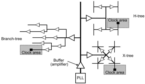
1.2.1
Conventional clock trees
The diagrams of a commonly used tree structures in clock distribution networks are shown in Fig.1.6. If the delays associated with each of the branches are equal, all receivers experience the same clock signal. The matching between different clock paths is the key point of the network design. In large area chips designed in advanced CMOS technology such a global matching is difficult to achieve.
Buffer (amplifier)
Clock area H-tree
X-tree Branch-tree
Clock area Clock area
PLL
Figure 1.6: Examples of conventional clock distribution tree structures: Branch-tree, H-tree and X-tree
Even if the positions of the receivers are symmetric with regard to the source point of the clock, mismatches between the buffers and the lines introduce uncontrollable skew. In practice, the local clock areas have different sizes and position, making difficult a perfect clock tree equilibrium. To solve the problem of the mismatch, the size of the lines and buffers must be increased so to become less sensitive to fabrication errors. However, this solution has a large power consumption penalty [68,7].
Despite the presented drawback, such a type of clock distribution techniques is widespread, in particular in middle-size low and average frequency chips (few hundreds of MHz), in some commercial processors [10,7], for local clocking of the different blocks of SoC, such as cache, ALU, etc.
1.2. State of the art: synchronous clocking in modern SoC 7
Clock mesh Driving buffer
PLL
Figure 1.7: Typical mesh clock network
Clock grid
A simple clock network with grid architecture is shown in Fig.1.7. The grid have the advan-tage of being relatively insensitive to the size and position of the receiver clock areas. The clock accuracy is mainly defined by the density and regularity of the grid geometry [1].
The dense grids demonstrate the best timing accuracy performance. Even if some grid lines are not perfectly positioned, the impact on the accuracy of the clock is negligible. How-ever, meshes can dissipate a lot of energy because they contain a large number of redundant lines whose capacity is high and by consequence, the associated switching power is substan-tial.
Skew compensation in clock trees
Improvements of the original tree distribution system consist in providing the clock generator with a skew compensation mechanism. It means that after the fabrication, mismatches and imperfections caused by fabrication errors are compensated and the final skew is diminished. Many skew compensation strategies have been proposed in the literature [58,72,13,32,
18,73,77,27,60], but only few of them have been used in practice.
In a centralized skew compensation technique, the skew monitoring and control are per-formed by a dedicated controller called skew compensator gathering information about the skew in all characteristic points of the chip. Its role is to ensure that the clock ticks sent to all clock domains arrive at the same time.
Fig.1.8presents the solution proposed in [27]. Each local synchronous clocking area has three connections with the compensator: a link to the direct path (forward path) and two links for the return (feedback path). The first link connect the clock source with the roots of each local tree. Two return signals are provided: one from the root of the local tree, on from one the leaves. The first return link is used to measure the round-trip time of the clock pulse, the second one is used to measure delay produced by the local tree. The compensator is capable to correct the phase error by increasing or decreasing the propagation time of the forward path. This approach has two principal drawbacks: the resolution of the measuring circuit is relatively low and the accuracy of the phase correction applied to direct path signals is limited. It is difficult to implement this strategy because of the requirements imposed on the
interconnections of the various regions. In addition, this strategy does not solve the problem of high power consumption associated with buffering of high frequency clock signals.
The decentralized approach of skew compensation technique is represented by imple-mentation described in [60]. This microprocessor uses a clock distribution network compris-ing two trunks. Each trunk is governed by its own clock tree (cf. Fig.1.9). It is possible to precisely adjust the clock in each trunk distributed through an variable delay line. A phase comparator (PC) located between the two trunks compares the arrival time of the clock ticks. In case of imbalance of clock ticks between two trunks, the delay of the distribution chain is adjusted via variable delay lines (VDL). This approach is particularly effective for compen-sation of skew associated with interconnections, and process, supply voltage, temperature (PVT) variations. Despite these advantages, this strategy requires global distribution of the high frequency clock, which should be buffered. Hence it requires a lot of power to keep the amplitude of the clock on appropriate level.
We note that neither centralized nor decentralized skew compensation technique solve the problem of the short-term jitter.
1.2.2
Optical distribution technique
The optical clock distribution is a promising alternative to the electrical one. Compared to the wires, the optical lines are not affected by cross talk with other on-chip signals. More-over, they are immune to noise sources of SoC, have higher bandwidth, timing accuracy and potentially consume less power than electrical distribution circuits [14]. The exam-ples of the research and analysis in the direction of optical distribution can be found in [9, 55, 64, 20, 41, 69]. The major electrical losses caused by the metal wires and buffers are avoided. Consequently, the interconnect delay is negligible and power consumption is trimmed. The example of structure of such a network is presented in Fig.1.10.
The main disadvantage of this approach is the problem of integration of optical circuits on a CMOS chip. Particularly, the study [11] highlighted several problems related to the performance of existing optical modulators, receivers and splitters in the CMOS silicon en-vironment. High performance photonic devices require special fabrication options, which
PLL Compensator
Region 1 Region 2
Region 3
1.2. State of the art: synchronous clocking in modern SoC 9 PLL VDL VDL Spines PC Driving buffer
Figure 1.9: Example of decentralized skew compensation technique proposed in [60]
Receiver circuit
Optical waveguides Local electrical clock distribution
Figure 1.10: An optical clock distribution network from [55]
increase the cost of the chip. The design flow remains fully custom since the EDA tools has not been developed yet. The studies [11, 14] show that for the effective realization of this approach, a significant efforts in study of materials and devices should be done. More recent research [65], confirmed a keen interest to this approach. The technological evolution reduced the number of integration issues, so that the test circuit has been implemented and tested. However, the question of formal and automated design flow remains open.
1.2.3
Multioscillator architectures
Multioscillator architectures implement multiple clock sources (oscillators) distributed over the chip area. Each oscillator generates the local clock for one SCA. The oscillators are synchronized with their immediate neighbors. When properly designed, the entire network is synchronized in frequency and in phase. Such an architecture has two advantages. First, the clock signal is regenerated locally, so the perturbations induced by long routed lines in tree architectures are avoided. Secondly, only neighboring oscillators are linked, so, there is no transmission of timing information on long distances.
There are two mechanisms of oscillator linking, i.e. coupling: in the energy domain (voltage/current) and the phase domain.
Injection locked oscillator networks
Injection coupling consists in injecting a part of the energy of one oscillator into the other, and vice versa. The injection coupling is a very old concept first discovered by Christiaan Huygens in far 1657. We present here two examples of clocking systems based on this mechanism.
Muzino et al. [42] present a comprehensive study of a distribution network based on a network of voltage controlled oscillators (VCO) coupled in the voltage domain (Fig.1.11). In this network the oscillators are coupled by equal length l transmission lines inserted be-tween their outputs. The oscillation frequency and phase are fixed by an external reference through a use of an analog PLL. The VCOs drive the local clock distribution network. This technique is analog, with typical weakness associated with analog circuits: a sensitivity to the perturbations, noises, fabrication mismatches, stability issues.
PC VCO VCO VCO VCO Vc l Local clock distribution network Global distribution networkVc /N Reference clock 1 1 2 2 Loop filter
Figure 1.11: Network of oscillators coupled by voltage presented in [42]: the number near each output of oscillator indicates the number of nearest neighbors
The research articles [46,56,57] propose to use a coupled oscillators network emulating a continuum in which can exist a standing wave. If the linear size of the chip is equal to the half wavelength, all points of the chip oscillate with the same phase, according to the physics of standing waves (Fig.1.12). The clock areas distributed over the chip use the local values of the standing wave as a local clock source. Again, the principal drawback of this approach is its analog nature: sensitivity to noises, to the geometrical disposition of the receivers, etc. Furthermore, the oscillation amplitude varies from one node to another: it is larger in the middle of the chip (at the anti-node of the wave) and smaller near the edges (at the nodes). This requires special receivers for the local clock recovery.
Networks of oscillators coupled in phase
The target quantity of the clock generators is the phase of the clock events: the energy of the oscillations, the waveform, etc. are not so important for the clock generation. Therefore, the
1.2. State of the art: synchronous clocking in modern SoC 11
Single SWO Virtual grounds
Prototyped clock grid Simulated clock grid Cross-coupled pair Injection-locked cross-coupled pair Clock buffer 14um 4um 3.5um 0.6mm 1.8mm Clkinj Accumulation-mode
MOS varactor transmission lineDifferential Cross-coupledpair
MUX and mixer Open-drain buffer
(a) (b)
Figure 1.12: Standing-wave clocking principle (from [46]): schematic (a), chip micropho-tograph (b)
N VCO
Reference N(N+1)2 [A] N N Local clocks
PC
Filter
Figure 1.13: Distributed PLL
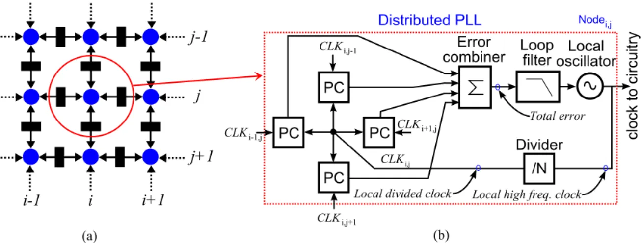
injection coupled network focus on what is not the most important for the clocking applica-tion. By contrast, the phase domain coupling considers only the information about the phase of the oscillators. The phase of an oscillator is the argument of the periodic function describ-ing the oscillator trajectory in the space of the state variable; the phase is hence an analog quantity. However, the phase can’t be measured directly; in general, the value of the phase is detected when the oscillation trajectory crosses a given plane, typically, the zero level of voltage/current. Hence, the phase is sampled. In addition, the instant of the phase detection can be considered as an event. Such a discrete event representation of the phase makes it less sensitive to the analog issues like perturbations, noises, etc. Moreover, a processing by digital circuit is possible. A network of oscillator coupled in phase is also called network of coupled phase locked loops (PLL), or a vector PLL. The idea of a clock generator based on a network of phase coupled oscillators has been proposed and developed in several studies [49,5,28,54,53,23].
A general architecture of a distributed PLL is presented in Fig.1.13. It contains N os-cillators, N loop filters and up to N(N+1)/2 phase comparators for comparison of the phases between any clock signals (local clocks and reference). In clocking applications, the net-work is a Cartesian mesh where the phase error detection is performed between the nearest neighbors. The system parameters must be chosen in a way so to synchronize the phase of the outputs of the oscillators with the reference signal.
A node of a PLL network includes a loop filter and a VCO (Fig. 1.14). The phase comparator compares the phase error between each couple of neighboring nodes. The use of such a system for clock generation was studied in [49], and a practical implementation was presented in [23].
F0 VCO Isochronous zone i PC PC PC /N Distributed clock F0/N from divider isochronous zone i+1
from divider isochronous zone i-1
/N
F0
Figure 1.14: Network node
Figure 1.15: 16-node distributed clocking network: (a) structure and (b) die microphoto-graph
signals at each node of the network. Phase comparators are situated at the boundary between neighboring local clock area (named tile in the original publication). They produce the error signals which are then summed and used to adjust the oscillation frequency of the node, as in Fig.1.14. It is shown in [49] that for the synchronization of all local clocks, it is necessary and sufficient to synchronize the clock of each node with the clocks of the neighboring nodes. Similarly to other mentioned above multioscillator systems, the analog implementation of such a solution is characterized by a low compatibility with modern SoC environment. In spite of the advantages of this approach, there is no industrial use of such a clock network, to our best knowledge.
1.2.4
Synchronous clocking architectures: conclusion
In this section we have studied few clocking approaches in modern VLSI systems aiming a global synchronization on GSLS chips. With the growth of the chip dimensions, the com-plexity of implementation of conventional and centralized clocking systems rises exponen-tially. Distributed decentralized clocking architectures seem more appropriate for large SoC,
1.2. State of the art: synchronous clocking in modern SoC 13
since they do not require chip-length wires for the global clock distribution. However, the principal drawback of the existing distributed clock generators is their analog nature, which makes them weakly compatible with the digital environment of the SoCs and with the stan-dard EDA tools existing for digital systems design.
The work presented in this PhD report focuses on multioscillator clocking architecture in which the oscillators are coupled in the phase domain. The principal contribution of this work consists in the study of fully digital implementation of the analog PLL networks originally proposed by Pratt, Nguyen, Chandrakasan and Gutnik [49,23].
1.3
Thesis outline and contribution
This PhD project studies an alternative clocking solution for large digital systems on chip: a network of all-digital PLLs is proposed for synchronization of local clocks of all synchronous clocking areas of the chip. The main advantage of this solution is the use of the local control loops for the global network synchronization. Moreover, the proposed solution is based on digital circuits, and is compatible with the environment of the SoC using the generated clock.
This document is organized as follows.
Chapter2presents the studied system. It describes the topology of the ADPLLs network and the architecture of the nodes, and discusses the issues related to the system-level design of the ADPLL network. In particular, the question of the selection of the desirable synchro-nization mode is addressed. The chapter ends with a summary of the specifications for each block of the network whose design is presented in Chapters3-5.
Chapter3 focuses on the development of a highly linear, compact, portable and recon-figurable 1-2.5 GHz 10 bit DCO based on a ring oscillator architecture. The whole design process is presented, starting from the system-level design down to the layout design. The chip has been fabricated in CMOS 65 nm technology and the measurement results are pre-sented.
Chapter4presents the design of the blocks measuring and processing the phase error: the digital phase comparator and the digital proportional-integral filter. The phase comparator has two particularities. Firstly, it measures not only the phase error but also the sign of the frequency error. For this reason it is called phase frequency detector. A formal character-ization of the frequency detection ability is provided. Secondly, the information about the phase/frequency error is provided in a digital form. The design of a 5 bit PFD with 32 ps resolution is presented.
To provide a working prototype demonstrating the proposed clock generation technique, a 4x4 ADPLL network in 65 nm technology has been designed. In order to validate the design before the chip fabrication, the network architecture has been tested on an FPGA platform. The two implementations are presented in Chapter5. The chapter is finalized with the results of measurements of the fabricated CMOS prototype.
The report is finished by conclusions and perspectives for the development and research associated with proposed clocking approach. The academic contribution consists in the arti-cles published and presented on international conferences.
Chapter 2
Network of distributed ADPLLs
Contents
2.1 Introduction . . . 15
2.2 Proposed clocking architecture. . . 16
2.3 Multiplicity of synchronisation modes . . . 25
2.4 Stability of the PLL networks . . . 29
2.5 Modeling of the clocking network . . . 30
2.6 Conclusion . . . 38
2.1
Introduction
In this chapter, we present an architecture of the multioscillator clock generator based on a network of distributed all-digital PLLs developed in this PhD project. The functionality of each block of the architecture is specified. This information is the input for the design of the prototypes presented in Chapter3and Chapter5.
In the first Section2.2we describe the topology of a PLL network for clock generation and we explain the principles of its operation. Then, we present the original idea of the PhD project: a digital implementation of the coupled PLL network for clock generation. Then, each block of the architecture is described, and their specifications are derived.
Large-signal nonlinear phenomena and stability issues are discussed in Section2.3 and Section2.4: these problems are related to the synchronization of the network, and are of first importance for the clock generation.
Section2.5describes the system-level behavioral model of the network and demonstrates the results of its system level simulation.
2.2
Proposed clocking architecture
2.2.1
Network of coupled PLLs
In 1995 Gill Pratt and John Nguyen proposed a distributed clock generator based on network of coupled analog PLLs [49]. Our work is based on this architecture. For this reason, this subsection provides essential information about it.
The proposed clock generator belongs to the family of multioscillator architectures based on a network of coupled oscillators. In such a clocking scheme, Fig.2.1, a chip is partitioned into local clock areas, each of them having its own clock generator (oscillator) which must be synchronized with its neighbors in the phase domain. The goal of the distributed PLL network is to synchronize each oscillator in phase and in frequency∗. In a steady state, such a network is a source of fully synchronous distributed local clocks.
(SCA)
Synchronous Clocking Area
Clock source with conventional
clock distribution chip boundary
Figure 2.1: Basic idea of multioscillator clocking approach
The architecture proposed by Pratt and Nguyen is a 2 dimensional Cartesian mesh net-work, where the nodes are the local clock generators and the arcs represent the coupling links between the local generators. Each local generator is linked only with its immediate Cartesian neighbors. Such a topology requires the shortest information transmission paths – which is a main advantage of such an architecture comparing with centralized clock genera-tion approaches.
The coupling between the oscillators is implemented in the phase domain via phase com-parators, Fig.2.2(a). Each phase comparator provides a measure of the error between the phases of two oscillators. This measure is then used by the control electronics associated with each oscillator in order to provide a control signal forcing the oscillators to synchro-nize with its neighbors. The control signal impacts directly the frequency of the oscillators – which is a derivative of the oscillator phase. For each oscillator a, the phase error ea,b is defined as the difference between its own phase and the phase of its neighbor b. The phase φ and the phase error are defined modulo 2π: the most common definition of the phase error is [49]:
ea,b= (π + φa− φb)mod2π − π. (2.1)
2.2. Proposed clocking architecture 17 CLKi,j Local oscillator Loop filter Error combiner j j-1 j+1 i i-1 i+1 (a) (b) Nodei,j Distributed PLL CLKi,j-1 PC CLKi+1,j PC CLKi-1,j PC CLKi,j+1 PC Divider /N Total error
Local high freq. clock Local divided clock
clo ck to cir cu itr y
Figure 2.2: Topology of the proposed clock network and architecture of the network node
According to this definition, ea,b can have values in the interval [−π, π]. The phase error
”seen” by the oscillator b between b and a is eb,a = −ea,b. For this reason, each phase
comparator is associated with two oscillators and generates two phase error signals e and −e. + Phase comparator Network interconnet Oscillator a CLKb CLK Oscillator bNode b Node a Node a Node b a ea,b -ea,b
Figure 2.3: Phase coupling between two oscillators
Fig.2.3presents an example of an autonomous (without input reference signal) network composed of two oscillators. In a more complex network, each oscillator i receives nierrors
with its nineighbors (Fig.2.2). These errors are processed by the control block including an
error combiner and a loop filter. The error combiner can be in the simplest case a weighted adder. The filter processes the combined error signal called Total error so to generate a control signal on the oscillator input. The objective of the control is to keep at the signal Total errorclose to zero.
It has been proved that such a system has a stable operation mode in which all oscillators have the same phase. The existence of this mode is conditioned by a right choice of the network parameters, in particular, the parameters of the control blocks of the nodes. It has been shown that apart the mode in which all oscillators have the same phase, there are several modes in which a fixed phase shifts between the oscillators exists. Pratt and Nguyen studied this phenomenon and indicated several solutions for the selection of the desirable stable synchronous mode. This issue is discussed in Section2.3.
The architecture proposed by Pratt and Nguyen has been successfully implemented by Gutnik and Chandrakasan [24]. The implemented chip contains 4x4 VCOs synchronized by
a PLL network.
The analog nature of this system is its main drawback for clock generation. The clock generator is usually integrated with the digital blocks which use the clock signal. The per-formance of an analog PLL in a digital environment may drastically degrade because of perturbations due to switching in the digital circuits. Moreover, using analog PLL network for clock generation makes more difficult a technology migration and reduces the design portability of the overall SoC.
The study of digital implementation of this architecture is the main focus of our work. This study aims to improve the portability, scalability and compatibility with the digital environment of the PLL network based clock generator. In the next subsection we present the principles of digital phase synthesis and its advantages for the distributed clock generation.
2.2.2
Digital phase synthesis
The principle of digital phase synthesis can be illustrated by the example of a single All-Digital Phase-Locked Loop (ADPLL). Known since a long time but actively used since one decade, the digital PLLs has recently gained ground on the analog PLLs [63]. The ADPLL operates following the same principle as their analog counterparts and functionally has the same structure (Fig.2.4).
Figure 2.4: Block diagram of the ADPLL
An analog phase comparator generating a signal proportional to the phase error is re-placed by a digital phase comparator (DPC), which generates a digital code proportional to the error. This code is processed by a digital loop filter (DLF). Thereafter, the signal from the filter output is used to control the VCO through a Digital-to-Analog Converter (DAC). The functions of the VCO and DAC are often integrated into a single block called Digitally-Controlled Oscillator (DCO). The divider defines the ratio between the reference (input) and output frequencies of the ADPLL, i.e. the frequency multiplication factor.
A digital PLL is a system processing mixed analog/digital signals: the target control quantity is analog (the phase), and the DCO and the digital phase comparators are DAC and ADC respectively. However, as it will be shown in the next two chapters, these two blocks can be implemented with digital cells. In addition, the phase is represented by the events of threshold crossing by the DCO output signal. Such a circuitry is weakly sensitive to the perturbations generated by digital circuit environment. Hence, the drawbacks usually associated with analog circuits are attenuated.
2.2. Proposed clocking architecture 19
A digital PLL has the following particular property. The phase error (the quantity to be regulated) is sampled by the divided DCO output signal; the same signal is used for the digital processing block clocking. However, the DCO output signal depends on what outputs the digital processing block. By consequence, an ADPLL is a self-sampled system. This fact significantly complicates the system analysis ; the properties of the ADPLL network related to the self-sampled operation were studied in the frame of the PhD project of Jean-Michel Akr´e [3]. Comparing with analog frequency synthesis, the digital phase synthesis has numerous advantages:
• Use of digital design techniques. Digital design costs less time and resources than analog design, thanks to the use of computer-aided design (CAD): automated synthe-sis, place and route flow.
• Reconfigurability and programmability. Digital implementation of the phase error processing block allows a use of complex processing algorithms not limited by simple PI or PID filtering as it is the case of the analog PLLs. An intelligence can be added to the clocking system: the control of the synchronisation mode, more effective filtering of perturbations, design-for-test (DFT) features, etc.
• Immunity to perturbations. The signals within the ADPLL network blocks are digi-tal: hence, they are less sensitive to the noise.
While a substantial expertise in the design of single ADPLLs has been accumulated dur-ing past decade, ADPLL network is a insufficiently studied system, particularly in what con-cerns its implementation in submicronic CMOS technologies. The next subsection present the architecture of the ADPLL network blocks.
2.2.3
Blocks of the ADPLL network
In this subsection we describe the architecture and discuss the basic parameters of the ADPLL blocks in the context of clocking network. We start from the oscillator, since it is the most critical block of the ADPLL system.
Digitally controlled oscillator
The oscillator in an ADPLL generates the output clock signal with the frequency defined by the input digital M-bit digital control word. As it is explained in Section 2.2.2, the DCO is generally a DAC whose output analog quantity is the frequency of oscillations at the output. In general the DCO DAC is supposed to be linear:
Fosc= F0+ ∆FK, (2.2)
where Fosc is the output frequency,∆F is the DAC resolution (the frequency step), K is the
value of the input code, F0 is the DCO initial frequency. A DCO is characterized by the
• Frequency tuning range. It specifies the upper and lower limits of the output signal frequency. In the context of clocking network it defines the tuning range of the clock frequency.
• Central frequency. This is the middle frequency of the frequency tuning range. In this project, the central frequency of the DCO defines the nominal frequency of the generated clock.
• Frequency tuning step. This parameter is the resolution of the DCO (cf. Eq. (2.2)). It defines the overall accuracy of the system (cf. the next subsection).
• Power consumption and area. These parameters are obviously critical for the clock-ing system. They are at the base of a figure of merit allowclock-ing a comparison of different clocking approaches.
• Input word width. This is the number of bits composing the input word. Together with the frequency tuning step this parameter defines the tuning range. This parameter has a direct impact on the complexity of the error processing blocks.
• Linearity/monotonicity. The transfer function of the oscillator relates the output fre-quency with the input code. This function is usually sought to be linear (cf. Eq. (2.2). For the PLL applications, a default in the linearity is not critical, since in the steady state mode the amplitude of an input DCO code is small. However, the error on lin-earity has the same impact as the error on the DCO gain. If the error is large, the performances of the PLL can be strongly affected.
The monotonicity of the code-frequency DCO characteristic is critical for the PLL application: a local inversion of the DCO characteristic slope sign is equivalent to an inversion of the PLL feedback sign. That immediately leads to an unstable behavior. Therefore, design techniques guaranteeing the monotonicity should be employed. • Phase noise. This parameter defines the jitter at the output of the DCO. Although the
DCO jitter directly impacts the quality of the generated clock, it is much less critical than in the RF applications. This allows a use of simple and ”economic” oscillator architectures such as ring CMOS (comparing with LC resonators required in RF archi-tectures).
Since the goal of our project is a proof of feasibility of the ADPLL network based clock generation, we do not focus on a design of DCO with state-of-the art performance. The most important characteristics of the DCO for this project are those critical for functional implementation of the network: in particular the parameters related to the frequency range, frequency step and monotonicity. The specification related issues will be discussed in Sec-tion2.2.4.
Loop Filter
The loop filter implements the processing of the phase error and the generation of the M-bit control digital word defining the frequency of DCO. Digital and analog PLLs employ proportional-integral (PI) or proportional-integral-derivative (PID) filters [22, 78, 16]. The
2.2. Proposed clocking architecture 21
study of Pratt and Nguyen demonstrated that a simple PI filter is a sufficient solution for synchronization of a PLL analog network. The studies of Akr´e et al. and Korniienko et al. demonstrated that this stands as well for digital PLL network [3,34,35,36].
This digital filter is a synchronous SISO (Single Input Single Output) digital signal pro-cessing block. Its operation is described by the equation:
H(z) = α + β 1 1− z−1 =
(α + β) − αz−1
1− z−1 (2.3)
whereα and β are the gain coefficients of the proportional and the integral paths respectively. The topology of the loop filter is shown in a Fig.2.5.
Figure 2.5: Block diagram of the PI filter
In a single ADPLL, the loop filter receives at the input the phase error between the input signal (the reference) and the DCO output. In the context of a network of ADPLLs, one node receives the errors between the local DCO and the neighboring nodes. The loop filter processes the combined value called Total error (cf. Fig. 2.2). In the simplest case the Total error is the sum of the errors with all neighbors, but more complex preprocessing is possible (weighted sum, shaping, selection of the link directivity, etc.). This preprocessing can satisfy specific requirements of the application, can be dynamically programmable. Its implementation is particularly easy in the digital version of PLL network.
Phase comparator
The phase comparator compares the phases of two clock signals and produces a digital N-bit code proportional to the phase error. The phase comparator is an ADC: its main character-istics are the dynamic range and the resolution. The analog phase comparator has a linear transfer function in a range between −π and π; an ideal digital phase comparator has the same quantized transfer function within the same range (Fig.2.6(a)). However, the PLL and the PLL network are designed so to have small errors in the normal operation mode: hence, a large dynamic range is not useful. Together with high resolution, it results in a high power and area cost. For this reason, the digital phase comparator may have an input range limited by certain value ∆φr (Fig. 2.6(b)). The phase comparator quantizes the phase error within
this range with resolution∆PFD.
When designing an ADC, the choice must be made in what concerns the interpretation of the input values inferior to the ADC resolution: are they considered as zero or one? In the
Code
PFD
(a) Code
(b)
1-bit offset saturation
Figure 2.6: Transfer function of the digital phase comparator: (a) equivalent of analog linear phase comparator and (b) linear phase comparator with limited range
first case, the ADC has a two resolution steps dead zone around the origin. In the second case, the sign of the error is correctly detected even for very small errors. For the digital phase comparator the second option is chosen, since in this case the phase comparator provides more information in the small error range (cf. Fig.2.6(b))
2.2.4
Specification of clocking network parameters
In this subsection we discuss the system-level specifications defining the constraints for the CMOS design of the ADPLL network. For the choice of these specifications we considered the typical parameters of the modern clocking systems. The discussed specifications are focused on the functional properties of the system such as the output frequency range and the clock error. We did not consider the constraints related to the size and with the power consumption of the blocks, seeking only a proof of the functional and physical feasibility of the architecture.
Frequency step and error processing rate
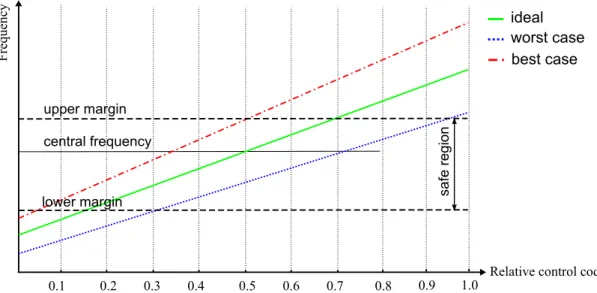
The most important specification having an impact on the system design is the clock fre-quency tuning step of the DCO and the error processing rate (the frefre-quency of the internal clock of the control block). These two parameters define the low limit of the output phase error (the tracking error of the regulation). The existence of a low limit of the tracking error is related to the discrete grid of the DCO output frequencies.
This phenomenon is illustrated in Fig.2.7, on the example of a single ADPLL. Let the input reference signal is periodic, with a linear phase evolution (dotted line). The phase of the DCO output signal must approximate as close as possible this trajectory. However, the output phase can only follow the lines with discrete slopes defined by the DCO frequency grid. The slope (the frequency) can change in function of the input DCO command word arriving with cadence 1/Ts. If the input reference frequency is not exactly one of the DCO
frequency grid values, an ideal control loop switches the DCO output frequency between two neighboring values (solid and dash-dot lines). There is a non-zero tracking error which can be minimized but never zeroed. It can be seen that the ”minimal” error is maximal when the reference frequency is exactly in the middle between two neighboring grid values. In this situation, the DCO frequency changes with each next input word, and the output phase error