HAL Id: hal-01887175
https://hal.archives-ouvertes.fr/hal-01887175
Submitted on 15 Oct 2018
HAL is a multi-disciplinary open access
archive for the deposit and dissemination of
sci-entific research documents, whether they are
pub-lished or not. The documents may come from
teaching and research institutions in France or
abroad, or from public or private research centers.
L’archive ouverte pluridisciplinaire HAL, est
destinée au dépôt et à la diffusion de documents
scientifiques de niveau recherche, publiés ou non,
émanant des établissements d’enseignement et de
recherche français ou étrangers, des laboratoires
publics ou privés.
Challenges for fully-integrated resonant switched
capacitor converters in CMOS technologies
Yasser Moursy, Anthony Quelen, Gaël Pillonnet
To cite this version:
Yasser Moursy, Anthony Quelen, Gaël Pillonnet. Challenges for fully-integrated resonant switched
capacitor converters in CMOS technologies. 2017 24th IEEE International Conference on Electronics,
Circuits and Systems (ICECS), Dec 2017, Batumi, Georgia. �10.1109/ICECS.2017.8292101�.
�hal-01887175�
Challenges for fully-integrated resonant switched
capacitor converters in CMOS technologies
Yasser Moursy, Anthony Quelen and Gaël Pillonnet
1CEA-LETI, Grenoble, France
Abstract—Switched capacitor (SC) converters inherent losses
limit the achievement of high efficiencies at high power densities for on-chip context. Hence, techniques are being investigated to enhance the deficient capacitance energy utilization. The resonant switched capacitor (ReSC) converters showed up as a promising candidate for efficient, dense, granular on-chip power supplies. In this paper, we discuss the design of ReSC converter employing integrated on-chip inductance in CMOS technology. We focus on a 2-phases 2:1 ReSC converter with single inductor. We discuss the practical constraints on using the on-chip air-core inductor and how it is going to affect the area of the converter. Using different inductor implementations, we compare the performance of the ReSC and SC converters of the same area. The results point towards the advantage of ReSC converter over the SC converter in case of using an inductor with relatively small area and negligible contact resistance which could be obtained in the 3D technology.
I. INTRODUCTION
The power delivery networks (PDN) to the integrated circuits become a bottleneck in the modern technologies. The monolithic integration of power supplies is increasingly attractive to divide the power conversion into multi-stages that consequently reduce the required number of converters and the power consumption of PDNs. Switched capacitor (SC) converters have been considered as the best candidate for the integrated power supplies as on-chip capacitors have a relatively high energy densities compared to inductance counterparts [1]. Also, the modern technologies allow the miniaturization of the capacitances while increasing the capacitance density [2]. However, the SC converters suffer from inherent charge-sharing losses and its switching frequency is considerably high to lower the output resistance.
Resonant switched capacitor (ReSC) converters are recently investigated in power on-chip context [3], [4]. They employ the same topology of the SC converter but comprise an inductor placed in the charging and discharging paths to create an adiabatic energy transfer which improves the efficiency. The resonance operation allows the reduction of switching losses by adopting the zero current switching and working at significantly lower frequencies with respect to SC converters with the same area while having the same output resistance [5]. In [6], [7], the ReSC converters are implemented with discrete inductors attached to the top of the die. Since the performance of ReSC depends on the inductance quality factor (Q), the usage of the discrete inductor with quality factor about 10-20 would be an
optimal solution. However, in [6], two discrete1.9 nH 0403HQ inductors were used to implement a two phase resonant switched capacitor converter. Due to the die-attaching, the equivalent series resistance with the inductor was increased from 0.038 Ω to about 0.2 Ω. This indicates that the inductor quality (L/R) has been degraded from 50 to 10. In addition to the contact resistance, an extra manufacturing step for mounting the inductor could be a burdensome and an expensive process for mass production that could limit the interests in these type of converters in fully integrated context.
This paper investigates the design of a fully integrated ReSC converter in 130 nm SOI technology to quantify the achievable performance. The fully integrated inductor could alleviate the external high contact resistance even if it suffers from an inherent low quality. We implement a 2-phases ReSC converter with only one inductor to reduce the area overhead and inductor resistance.
The paper is organized as follows, Section II discusses the operation of the resonance switched capacitor converters. Section III illustrate the challenges in the implementation of the integrated inductor. Transistor-level simulation results are reported in Section IV.
II. RESONANT SWITCHED CAPACITOR CONVERTER OPERATION
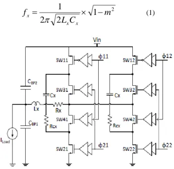
The 2:1 ReSC converters topologies can be generally categorized into single-ended and multiphase topologies. In each category, the circuits can be classified based on the inductor position [6]. In presence of a large parasitic inductance, which results from the bonding wires, large supply input current variations fluctuate the supply voltage of the single-ended topology that degrades the overall system efficiency. In order to solve this issue, the multiphase topology is used. A two phases ReSC converter is shown in Fig. 1 [8]. The phase shift between the two phases is 180°. The current drawn from the supply (Iin) is relatively constant (Iin ≈ ILoad/2)
which reduces the supply voltage variations in the presence of parasitic inductors.
Such architecture is of interest since it employs only one inductor for two phases, hence, the number of integrated magnetic components is reduced. The resonance frequency can be expressed as follows:
2
1
2
2
1
m
C
L
f
x x x
(1)Fig. 1. 2-phases ReSC converter based on one inductor.
where Lx and Cx are the inductor and flying capacitor occupying
an area A. m is the damping factor of the circuit which is defined as:
𝑚 = 𝑅𝑡𝑜𝑡 2 √
𝑁 × 𝐶𝑥
𝐿𝑥 (2)
where N is the number of parallel phases which is 2 in this case and Rtot is the total resistance in the charging or discharging
paths which can be expressed as:
𝑅𝑡𝑜𝑡 =2𝑅𝑆𝑊 𝑁 +
𝑅𝑐𝑥
𝑁 + 𝑅𝑥 (3) where RSW is the on-resistance of the switches, Rcx is the
capacitor Cx equivalent series resistance, and Rx is the inductor series resistance. The converter’s output resistance can be expressed as follows: 𝑅𝑒𝑓𝑓= 𝜋𝑅𝑡𝑜𝑡 4𝑚√1 − 𝑚2∙ tanh ( 𝜋𝑚 2√1 − 𝑚2) ≈ 𝜋 2 8 ∙ 𝑅𝑡𝑜𝑡 1 − 𝑚2 ≈ 𝜋2 8 ∙ 𝑅𝑡𝑜𝑡 (4)
Reff models the conduction losses in the converter. The
approximations in (4) consider that m is relatively small (m<0.2).
The efficiency of the converter can be expressed as: 𝜂 = 1 − 𝑃𝑐𝑜𝑛𝑑 𝑃𝑖𝑛 − 𝑃𝑠𝑤 𝑃𝑖𝑛 = 1 − 𝐼𝐷𝐶 𝑣𝑜𝑁𝐿∙ 𝑅𝑒𝑓𝑓 − 4𝑁 ∙ 𝐶𝑠𝑤∙ 𝑉𝑔2∙ 𝑓𝑥 𝐼𝐷𝐶∙ 𝑣𝑜𝑁𝐿 (5)
where Pin is the input power, Pcond and Psw are the conduction
and switching losses in the converter, voNL is the no-load output
voltage, IDC is the DC output current, Csw is the gate capacitance
of switches, and Vg is the switches’ gate voltage swing. From (5), the sizes of switches are inversely proportional to the conduction loss and directly proportional to the switching loss.
Hence, for a certain load current, the sizes of the switches have to be optimized in order to balance switching and conduction losses and hence maximize the efficiency at this load current.
III. INTEGRATED INDUCTOR DESIGN
Since the ReSC conduction loss is a function of the total resistance in the charging or discharging paths as shown in (5), the inductor resistance should be minimized. The integrated air-core planar inductance depends on its area [9], hence, the inductor’s area should be maximized in order to increase the inductance. When scaling the inductor area by a factor ", while maintaining the same geometrical aspect ratio, the inductance is scaled by √𝜀 while the resistance remains unchangeable. Consequently, the damping factor is increased by 𝜀1/4. Thus, the chip should comprise the minimum number of inductors with minimum resistance in order to achieve a relatively low damping factor and reduce the mutual coupling between the on-die inductors.
Using a thick metal option of 3 μm thickness in 130 nm technology, assuming an area of 2mm2 dedicated for the
implementation of an inductor, a 1.6 nH square planar air-core inductance is realized as depicted in Fig. 2. Using Momentum- Virtuoso for post-layout inductance characterization, we compare between this planar air-core inductor without MIM capacitors underneath it, on-die solenoid with magnetic core [10], and discrete air-core inductor with 0302 CS package as depicted in Table I. The damping factors of the integrated inductors are relatively high compared to the discrete one. However, the main issue concerning the discrete inductor is its mounting process and the access resistance and capacitance in addition to the pinout increase. The integrated magnetic core inductors have a higher scalability and can be realized on ultra-thin package dies. Also, it would be better from the volume power density point of view. However, we are not going to use the typical CMOS technology and the current is limited by the saturation current. It also should be noted that the metal thickness used in the magnetic core inductor is about two times larger than the one used in the air core inductor [10].
TABLE I: Comparison between different inductors around operating frequency 70 MHz.
L1 L2 [10] Discrete Units Inductance 1.6 1.5 1.7 nH AC impedance 180 250* 38** mΩ Area 2 0.1* 0.46 mm2
Metal trace width 300 - - µm Metal trace thickness 3 6 and 12 - µm Unloaded damping factor 0.125 0.125 0.017–0.025 -
* Parameters are given at frequency of 100MHz and the area is estimated from the given data in [10].
** Measured in frequency range of 20-40MHz [3]
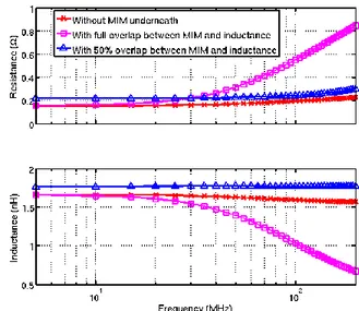
In order to minimize the area overhead and increase the power density, the inductor should occupy the same area as the full chip. The MIM capacitors used in the implementation of the the flying and bypass capacitors lays underneath the
inductance. To evaluate this proposition, simulations are done with and without MIM capacitors in order to estimate the inductance and its parasitic resistance. For the simulation purposes, we reduce the complexity of the layout, as shown in
Fig. 2. Illustration for the layout of the planar inductor with MIM capacitors underneath it at 50% overlap configuration. The capacitor plates are not to scale.
Fig. 2, by only including an inductor implemented on thick metal (M6), a shield for the inductance implemented on metal M5, not shown in figure, and metal elements representing the top plate of the MIM on metal M4.
In Fig. 3, the Momentum-Virtuoso results show the inductance and resistance values of the integrated inductor versus the frequency. There is a significant increase in the inductance’s resistance when the MIM capacitors are totally overlapped with the inductance. This resistance increase comes from the magnetic field lines that have to cross the metal layers underneath resulting in eddy currents that generate magnetic field oppose the original one. Hence, the inductance value is reduced and its parasitic resistance is increased. Consequently, the full overlap of the inductor and capacitance area is not feasible from the efficiency point-of-view. When 50% overlap is used, the percentage increase of the inductor’s resistance relative to its original value is 29% at frequency of 70 MHz. However, this ratio is about 130% in case of the 100% overlap case at the same frequency. Therefore, if we assumed 50% overlap, half of the area of the inductance is added to the capacitance area. For a fair comparison between the ReSC and SC converters, we assume that the inductor additional area is going to be replaced by the flying capacitors. For example, if we have a design of 1mm2 and the inductance is 1mm2, if we
assumed 50% overlap then the total design area becomes 2mm2 for ReSC converter. However, for the SC, the design area is the same with the additional 1mm2 dedicated for the
implementation of extra flying capacitors.
Fig. 3. Post-layout simulation comparison between planar inductor value with and without MIM capacitors underneath.
IV. TRANSISTOR-BASED SIMULATION RESULTS
The design specifications of the proposed converters are shown in Table II. The die area is shared between the bypass and flying capacitors. All the capacitors are considered to be implemented using double MIM capacitors with capacitance density of 4 fF/μm2.
TABLE I: Comparison between different inductors around operating frequency 70 MHz.
Vin 1.8 V Vo (min.) 0.7 V Area 2 – 3 mm2 Max. Inductor
area
2 mm2
CFly ReSCC 2 x 2 nF CBP ReSCC 2x2 nF CFly SCC1 2x2 nF Switching freq. 65 MHz CFly SCC2 2x3 nF CBP SCC 2x2 nF
Fig. 4 shows the simulation results of the efficiency versus the power density at different load resistances using several inductors. The first case, we assume the presence of an inductor with small form factor similar to the integrated magnetic core inductor previously shown. The area of the chip is 2mm2 hence,
the flying capacitor is 2 nF. The ReSC converter has a peak efficiency of 72% at 70 mW/mm2 while the SC converter has
an efficiency of 60% at the same power density. The second case, if we used an on-chip inductance is realized with 50% overlap with the capacitance, hence, the total area of the chip is 3mm2. In order to achieve a fair comparison, the flying
capacitor in the SC converter is assumed to occupy the additional area of the inductor. Consequently, the flying capacitor in the SC is 3 nF per stage. In this case, the SC converter outperforms the ReSC since it has a lower output
resistance compared to the SC converter at the same operating frequency. These results highlight the importance of having an inductor with relatively small dimensions compared to the chip
Fig. 4: Efficiency versus power density for different ReSC topologies.
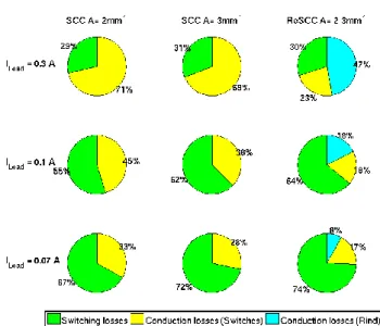
Fig. 5: Losses analyses for SC and ReSC converters at different load currents.
and hence, the ReSC converters are able to cover a wider range of power density while achieving higher efficiency compared to the switched capacitor converter.
Fig. 5 shows the percentage loss breakdown in the SC and ReSC converters. The ReSC converters with different area are going to have the same loss since the additional area in the 50% overlap is not having any additional active components. In case of high load currents, the conduction loss dominates in the two types of converters. However, the largest percentage of loss in ReSC converter is due to the inductor conduction loss. This signifies the necessity of having a low inductor resistance in ReSC converters. In case of light load currents, the switching
losses dominates, however, we still have a percentage of loss due to the inductor that can be optimized in ReSC converters.
V. CONCLUSION
The implementation of the resonant switched capacitor (ReSC) converters has been discussed. The key to achieve high efficiency along with high power densities is the inductance implementation and its resistance. Thus, several inductance implementations are considered to compare their areas and resistances. First, using discrete inductor which has a high quality factor mounted on-chip in spite of that it suffers from high resistance due to bonding connections and high cost due to the extra-manufacturing step. Secondly, using on-chip air-core inductor that eliminates the manufacturing complexity yet it increases the area and has a relatively poor quality factor. Finally, using modern integrated magnetic technologies to realize compact inductors with relatively small area which could be of interest to achieve high efficiencies at high power densities. The results shown illustrated the effect of the additional inductor area on the power density and how it moves the ReSC converter to lower power densities using standard CMOS technology. The salient features of the ReSC converters require an efficient inductor with relatively small area which would feasible in the 3D technology.
REFERENCES
[1] S. R. Sanders, E. Alon, H. P. Le, M. D. Seeman, M. John, and V. W. Ng, “The Road to Fully Integrated DC-DC Conversion via the Switched-Capacitor Approach,” IEEE Transactions on Power Electronics, vol. 28, no. 9, pp. 4146–4155, Sep. 2013.
[2] G. Pillonnet and N. Jeanniot, “Effect of CMOS Technology Scaling on Fully-Integrated Power Supply Efficiency,” in CIPS 2016; 9th International Conference on Integrated Power Electronics Systems, Mar. 2016, pp. 1–5.
[3] K. Kesarwani, R. Sangwan, and J. T. Stauth, “4.5 A 2-phase resonant switched-capacitor converter delivering 4.3w at 0.6w/mm2 with 85% efficiency,” in 2014 IEEE International Solid-State Circuits Conference Digest of Technical Papers (ISSCC), Feb. 2014, pp. 86–87.
[4] C. Schaef, K. Kesarwani, and J. T. Stauth, “20.2 A variable-conversion ratio 3-phase resonant switched capacitor converter with 85% efficiency at 0.91w/mm2 using 1.1nh PCB-trace inductors,” in 2015 IEEE International Solid-State Circuits Conference - (ISSCC) Digest of Technical Papers, Feb. 2015, pp. 1–3.
[5] G. Pillonnet, “Modeling and efficiency analysis of multiphase resonant-switched capacitive converters,” IEEE Transactions on Power Electronics vol. 31, no. 1, pp. 11–14, 2016.
[6] K. Kesarwani, R. Sangwan, and J. T. Stauth, “Resonant-Switched Capacitor Converters for Chip-Scale Power Delivery: Design and Implementation,” IEEE Transactions on Power Electronics, vol. 30, no. 12, pp. 6966–6977, Dec. 2015.
[7] L. G. Salem and P. P. Mercier, “A single-inductor 7+7 ratio reconfigurable resonant switched-capacitor DC-DC converter with 0.1-to-1.5v output voltage range,” in 2015 IEEE Custom Integrated Circuits Conference (CICC), Sep. 2015, pp. 1–4.
[8] K. Kesarwani and J. T. Stauth, “The direct-conversion resonant switched capacitor architecture with merged multiphase interleaving: Cost and performance comparison,” in 2015 IEEE Applied Power Electronics Conference and Exposition (APEC), Mar. 2015, pp. 952–959.
[9] S. S. Mohan, M. del Mar Hershenson, S. P. Boyd, and T. H. Lee, “Simple accurate expressions for planar spiral inductances,” IEEE Journal of solid-state circuits, vol. 34, no. 10, pp. 1419–1424, 1999.
H. K. Krishnamurthy, V. Vaidya, S. Weng, K. Ravichandran, P. Kumar, S. Kim, R. Jain, G. Matthew, J. Tschanz, and V. De, “20.1 A digitally controlled fully integrated voltage regulator with on-die solenoid inductor with planar magnetic core in 14nm tri-gate CMOS,” in 2017 IEEE International Solid-State Circuits Conference (ISSCC), 2017, pp. 336– 337.