HAL Id: hal-01149528
https://hal.archives-ouvertes.fr/hal-01149528
Submitted on 25 Jun 2018HAL is a multi-disciplinary open access
archive for the deposit and dissemination of sci-entific research documents, whether they are pub-lished or not. The documents may come from teaching and research institutions in France or abroad, or from public or private research centers.
L’archive ouverte pluridisciplinaire HAL, est destinée au dépôt et à la diffusion de documents scientifiques de niveau recherche, publiés ou non, émanant des établissements d’enseignement et de recherche français ou étrangers, des laboratoires publics ou privés.
Fabrication and photoluminescence properties of
Tb-doped nitrogen-rich silicon nitride films
Y.-T. An, C. Labbe, M. Morales, P. Marie, F. Gourbilleau
To cite this version:
Y.-T. An, C. Labbe, M. Morales, P. Marie, F. Gourbilleau. Fabrication and photoluminescence properties of Tb-doped nitrogen-rich silicon nitride films. physica status solidi (c), Wiley, 2012, E-MRS 2012 Spring Meeting – Symposium A, 9 (10-11), pp.2207. �10.1002/pssc.201200253�. �hal-01149528�
properties of Tb-doped nitrogen-rich
silicon nitride films
Y.-T. An, C. Labbé*, M. Morales, P. Marie, and F. Gourbilleau
CIMAP, UMR CNRS/CEA/ENSICAEN/UCBN, 6 Boulevard Maréchal Juin, 14050 Caen Cedex 4, France
Keywords: magnetron sputtering, nitrogen-rich silicon nitride, Tb3+, photoluminescence
*Corresponding author: e-mail christophe.labbe@ensicaen.fr
Terbium (Tb) doped nitrogen-rich silicon nitride thin films were prepared on [100] Si substrate by reactive magnetron co-sputtering in pure nitrogen atmosphere. The microstructure and optical properties of the films were investigated by means of ellipsometric spectroscopy (ES), atomic force microscopy (AFM), X-ray diffraction (XRD), Raman scattering and Fourier transform infrared (FTIR) spectroscopies as well as by photoluminescence (PL) experiments. A notable
emission from Tb3+ ions was obtained for the
as-deposited layer, while the maximum intensity was found from 600 °C-annealed sample. Deducing from PL excitation (PLE) analysis, a mechanism of excitation of Tb3+ ions was proposed: the band tail states of matrix
play a minor role in the energy transfer process, while the host carriers across the optical gap acted as effective sensitizers for Tb3+ ions.
1 Introduction Si-rich silicon nitride (SRSN)
material has received great interest in the last decades. Its lower band gap and larger density of trap states are in agreement with the need of low injection voltages for applications in light emitting diode (LED) devices [1, 2]. Moreover, the Si excess can form Si nano-clusters which contributes to visible photoluminescence but can plays sensitizing role towards rare earth (RE) ions too [3, 4].
In contrast to SRSN, nitrogen-rich silicon nitride (NRSN) films are also considered as a promising candidate for LED devices, as they show better interface properties when used in silicon-based metal-insulator-semiconductor devices and have better negative charge ability and stability [5]. The NRSN layers have been deposited by many groups using a conventional approach of plasma enhanced chemical vapor deposition (PECVD) [5-7]. In this case, the film composition was tuned through the SiH4/NH3 ratio. Such a film presents numerous band tail
states and small band gap [8] which can play the role of sensitizer for RE ions. Tb3+ ions offer an interesting green
emission at a 543 nm wavelength for future Si-based LED devices. Yuan et al. [7] have evidenced an efficient energy transfer from matrix to Tb3+ ions in Tb-implanted silicon
nitride layer fabricated by PECVD. The same process has
been demonstrated in Tb-doped silicon oxynitride matrix [9].
In this study, we deposited films by means of reactive magnetron sputtering of a Si target toped with Tb4O7 chips
in pure N2 plasma. The sputtered Si atoms react with N2 in
the plasma to allow the growing of a NRSN matrix. The structural properties of the layers were characterized by various methods such as X-ray diffraction (XRD), ellipsometric (ES), and Raman scattering spectroscopies. Room temperature PL as well as dynamic PL behavior was investigated as a function of annealing temperature (TA).
The energy transfer mechanism was also analyzed by means of PL excitation (PLE) experiments.
2 Experimental details The films were grown on
p-type 250 μm-thick [001]-Si single crystalline wafers by reactive magnetron co-sputtering of a pure Si target topped with a given number of Tb4O7 chips under pure nitrogen
plasma at a pressure of 23 µbar. The substrate temperature and RF power density were fixed at 200 °C and 5 W·cm-2,
respectively. The annealing of the deposited thin layers were performed in a conventional furnace in a 500-1100 °C range for 1 h in a dry nitrogen flow.
The refractive index and the thickness were deduced from ES with an incident light ranging from 1.5-4.5 eV by using a Jobin-Yvon ellipsometer. The sample structure was studied using XRD and Raman spectroscopy. The XRD measurements experiments were performed using a Philips Xpert NPD Pro diffractometer mounted with a point scintillation detector in the θ-2θ configuration. Raman spectra were measured with 532 nm continuous waver laser by means of Dispersive Horiba Yvon Raman spectrometer equipped with confocal microprobe and CCD camera. For this latter, the experiments were performed on films deposited on fused silica substrates instead of silicon ones. The infrared absorption properties were investigated by means of a Nicolet Nexus Fourier Transmission Infrared (FTIR) spectroscopy in 500-4000 cm-1 range. The
PL emission and PLE measurements were carried out using a 450 W xenon arc lamp as excitation source at room temperature with help of Jobin-Yvon Fluorolog spectrometer. The lifetime was obtained by means of an optical parametric oscillator with a pulse of 5 ns at full width at half maximum and a repetition rate of 10 Hz for a 244 nm wavelength excitation. The spot diameter was 500µm with an average energy of 15 mJ.
3 Results and discussion
3.1 Film microstructure The refractive index was investigated by ellipsometric spectroscopy and fitted by an effective medium approximation model. For the as-deposited sample, the refractive index was 1.71 at 1.95 eV. This value was quite lower than that of stoichiometric Si3N4 (about 2.04) at this energy [10], which is the
signature of the growth of Nitrogen-rich-Silicon Nitride film (NRSN) [8]. To be sure that this lower refractive index is not the result of an important roughness resulting from the reactive deposition process [11], atomic force microscopy observations (image not shown here) were performed. The layer surface presents root mean square roughness values less than 1 nm attesting that the produced layer is the expected NRSN film.
1300 1200 1100 1000 900 800 700
A
b
s
o
rbanc
e (
a
.u
.)
W avelength (nm )
B rew ster's incidence as-deposited film 6 G aus s ian peaks f it ν3 ν 2 ν1Figure 1 FTIR spectrum of as-deposited film recorded at Brewster angle (65°).
Figure 1 depicts a typical FTIR spectrum recorded at Brewster incidence (65°) for the as grown film. This spectrum was fitted with six Gaussian curves centered at 825, 860, 1020, 1070, 1161 and 1225 cm-1, respectively.
The main absorption peaks located at 860 (TO), 1020 (TO), and 1161 (LO) cm-1 were attributed to Si-N asymmetric
stretching mode named as ν1, ν2 and ν3, respectively. It is
reported that the blueshift of the Si-N stretch mode was agreed with the increase of nitrogen content in silicon nitride film [12-14]. Bustaret et al. [12] reported in
addition the main Si-N bonds at 850 cm-1, a strong
shoulder in the 970-1010 cm-1 range grown with nitrogen
content. Our sample had a much higher ν2 TO Si-N
position at 1020 cm-1 which is evidence that we have
grown a NRSN film. The other three peaks, in Fig. 1, located at 1225 cm-1 (LO
3), 1070 cm-1 (TO3), and 825 cm-1
(TO2 and LO2) in blue dashed line are all assigned to Si-O
bonds. The presence of oxygen atoms in the film is attributed to the sputtering of the Tb4O7 chips used.
200 300 400 500 600 700 20 40 60 80 In te n s ity ( a .u .) 2 theta (degrees)
In
te
n
s
ity
(
a
.u
.)
Raman shift (cm
-1)
T
A=1100°C
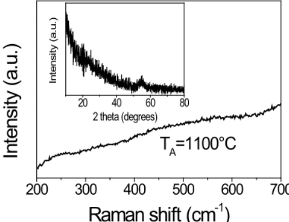
Figure 2 Raman spectrum on fused silica sample annealed at
1100 °C. The inset showed XRD pattern of Tb-doped film annealed at 1100 °C.
The Raman analysis was performed on an 1100 °C-annealed film grown on fused silica substrate (Fig. 2).
No peak appears at 520 cm-1 which means that no
crystallized Si grains are present in the layer. This is confirmed by the XRD experiments (inset of Fig. 2) which do not show any peak issue from the diffraction on Si planes. The presence of a peak at 55° is attributed to the substrate. These microstructural investigations attest the amorphous nature of the annealed layer even after a high temperature annealing process [15, 16].
3.2 PL spectroscopy
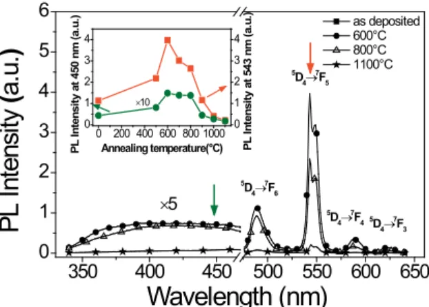
The PL behavior of the films was explored for the different annealing temperature using an excitation wavelength of 325 nm (Fig. 3). Four emission peaks in the 480-640 nm range and a broad band emission with lower intensity compared to the Tb3+ PLintensity have been detected. Such
broad emission band which is usually attributed to the band tails states [8] is expanded to 340 nm due to the composition in our film.
350 400 450 500 550 600 650 0 1 2 3 4 5 6 0 200 400 600 800 1000 0 1 2 3 4 0 1 2 3 4 P L In te n s it y a t 5 4 3 n m ( a .u .) P L In te n s it y a t 4 5 0 n m ( a .u .) Annealing temperature(°C) ×10 5 D4→ 7 F3 5 D4→7 F4 5 D4→ 7 F5
P
L
In
te
n
si
ty
(
a.
u.
)
Wavelength (nm)
as deposited 600°C 800°C 1100°C ×5 5 D4→ 7 F6Figure 3 PL spectra excited at 325 nm for different annealing
temperature. Inset is PL intensities at 543 nm (Tb3+) and 450 nm
(band tail states) as a function of the annealing temperature.
The PL intensity increases with TA to reach the
maximum in the 600-800 °C range and then decreases for highest annealing temperatures. Concerning the four peaks are centered at about 488, 543, 590, and 621 nm, they correspond to the intra-4f 5D
4→7F6, 5D4→7F5, 5D4→7F4
and 5D
4→7F3 transitions of Tb3+ ions, respectively. One
can notice the presence of a significant emission from Tb3+
ions even for the as-deposited sample. The maximum emission of Tb3+ is achieved after an annealing treatment
at 600 °C following by a decrease for higher TA (inset of
Fig. 3). Band tails and Tb ions emissions present the same evolution with the annealing temperature. The behavior for the low TA range is explained by the fact that the annealing
treatment decreases the nonradiative recombination rates and consequently increases the PL intensity of both host matrix and Tb3+ ions [17]. Annealing above 600 °C favors
the Tb agglomeration, which, consequently, quench the Tb emission [18]. In the same time, no increase of the band tails emission is observed at high temperature. This annealing treatment in a nitrogen flow should favor the rearrangement of the matrix leading to the recovering of the radiative defects and thus can explain the quenching observed in 350-460 range. It is worth to note that the Tb3+ luminescence decay at 1000 °C (not shown here) is characterized by a stretch exponential decay with a life time of almost 600 µs at 543 nm. Such a value agrees with those achieved in Tb-doped films annealed at this temperature [9].
The Fig. 4 depicts the PLE spectra collected for the broad band emission at 390 or 450 nm and for the Tb-emission wavelengths at 488 and 543 nm for sample
annealed at 600 °C. The Tb3+ PL showed an overall
increase with the decreasing of excitation wavelength (from 480 to 265 nm). Two clear peaks were observed in the Tb-PLE spectra, locating at around 265 and 330 nm, respectively. The PLE spectra reflect the absorption of the different elements constituting the matrix. In fact, the
200 250 300 350 400 450 500 0 1 2 3 4 5
P
L
E
In
te
n
si
ty
(
a
.u
)
Wavelength (nm)
Tb3+ PL intensity at 543 nm at 488 nmBand tails PL intensity
at 450 nm at 390 nm
T
A=600°C
×10
Figure 4 PLE spectra of 600 °C-annealing sample monitored at
543 nm, 488 nm (Tb3+ related) and 450 nm and 390 nm (band
tails).
typical absorption spectrum for rare earth in the absence of energy sensitization process from host matrix should appear as a set of discrete peaks, corresponding to the inhomogeneous broadening of Tb ions [19]. Our Tb-PLE spectra do not reveal any well-defined peaks. This implies that Tb3+ ions are not resonantly excited in the UV range
(250-400 nm) but underlines an energy transfer coming from other elements of the matrix to Tb3+ ions.
The broad band PLE spectra of the band tails (red triangle) showed the same peak position at 265 nm. This result was the same as that of Tb with detection at 488 nm in black line. Therefore, the PLE spectra of both matrix and Tb appeared to have a similar contribution from a strong peak at 265 nm (4.7 eV), which suggests a presence of high efficient energy transition. In other words, the major contribution for the Tb-PL comes from this transition that could arise from the N pπ lone pair states near the valence band in NRSN films [20].
The film studied in this work was considered to hold ~4.7 eV optical Tauc gap according to our refractive index, which agreed well with the previous reported values of silicon nitride [2, 8]. Therefore, in the Tb-PLE spectra the peak at 4.7 eV should come from the carriers across the optical gap into the extended states-carriers that could be
captured directly by Tb3+-related states [9]. As a
consequence, the carriers in the extended N pπ states played the main sensitizer role of Tb3+ ions. The PLE roll
off at high photon energies excitation can be attributed to the reducing of the energy transfer efficiency due to the carrier thermalization into efficient nonradiative trap states [21].
The PLE peak of Tb ions at 330 nm observed in the case of Tb ions is attributed to the band tail absorption in the NRSN matrix [7]. The two wavelengths detection at 390 nm and 450 nm described two different PLE peaks centered at 340 and 360 nm, respectively. This shifting behavior with the detecting wavelength is feature of states density due to the filling of the band tail states.
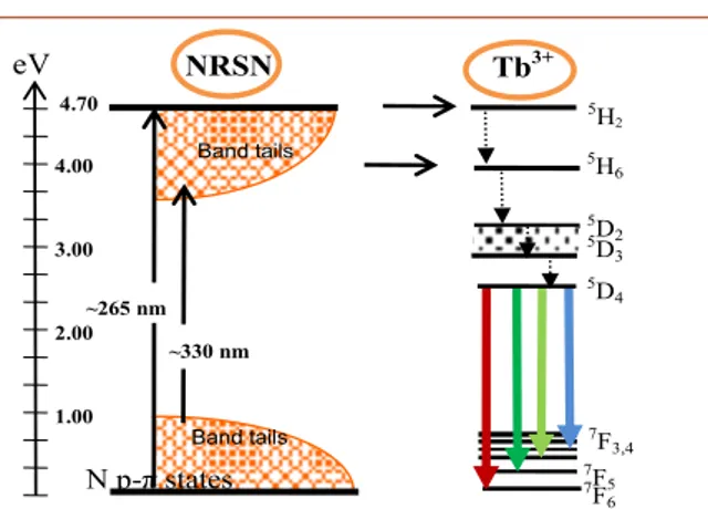
~265 nm 7F 6 7F 5 7F 3,4 Band tails Band tails N p-π states ~330 nm eV 4.70 1.00 2.00 4.00 3.00 NRSN Tb3+ 5H 2 5H 6 5D 2 5D 3 5D 4
Figure 5 Schematic band diagram of the Tb-NRSN film with a
mechanism proposed to explain the PL in the NRSN film.
In the light of these results, a qualitative model is proposed here to explain the optical behavior observed in our films, as shown in the scheme (Fig. 5). There are two main energy transfer mechanisms identified between
matrix and Tb3+ ions. When excited around 265 nm,
corresponding to the gap at 4.7 eV, the carriers mediated in
matrix are excited and an energy transfer to the Tb3+
excited states 5H
2 occurs. It is followed by the
non-radiative relaxation from states 5H
2 to 5D4 and then to
the ground states with four peak emissions. When excited energy is lower than the gap, carriers trapped in the band tails states can transfer weak energy to Tb3+ ions.
4 Conclusions The films were deposited by sputtering method and attested as NRSN by low refractive index, the absence of crystalline grains and the blueshift and broaden shoulder for Si-N bonds in FTIR spectroscopy. The strong Tb3+ emission was obtained by optimizing the
annealing condition. On the basis of PLE spectra, two processes of energy transfer to Tb3+ may exist: band tail
states, carrier mediated. Furthermore, the carrier mediated was considered to play a main role in obtaining high Tb emission and band tail states act a supporting role.
Acknowledgements The authors would like to thank Dr.
Sophie Boudin from CRISMAT lab with the measurement of PL
and PLE spectra. This work is supported by the contract CEA/DSM/HOFELI and the program of Chinese Scholarship Council (CSC).
References
[1] L. Dal Negro, J. H. Yi, and L. C. Kimerling, Appl. Phys. Lett. 88, 233109 (2006).
[2] M. Wang, J. Huang, and L. Pavesi, J. Appl. Phys. 104, 083505 (2008).
[3] R. P. Nalini, L. Khomenkova, and F. Gourbilleau, Nano-scale Res. Lett. 7, 124 (2012)
[4] E. Steveler, H. Rinnert, and M. Vergnat, Appl. Phys. Lett.
97, 221902 (2010).
[5] Y. L. Ren, K. J. Weber, and N. M. Nursam, Appl. Phys. Lett.
98, 122909 (2011).
[6] L. Wang, H. S. Reehal, and A. del Prao, Semicond. Sci. Technol. 18, 633 (2003).
[7] Z. Z. Yuan, D. S. Li, and D. R. Yang, J. Appl. Phys. 100, 083106 (2006).
[8] J. Kistner, X. Chen, and J. H. Werner, J. Appl. Phys. 110, 023520 (2011).
[9] H. Jeong, S. Y. Seo, and J. H. Shin, Appl. Phys. Lett. 88, 161910 (2006).
[10] T. Baak, Appl. Optics 21, 1069 (1982).
[11] G. Xu, P. Jin, and K. Yoshimura, Thin Solid Films 425, 196 (2007).
[12] E. Bustarret, M. Besouda, and S. C. Gujrthi, Phys. Rev. B
38, 8171 (1988).
[13] C. Sénémaud, A. Gheorghiu, and S. Gujrathi, J. Non-Cryst. Solids 164, 1073 (1993).
[14] K.-C. Lin and S.-C. Lee, J. Appl. Phys. 72, 5474 (1992). [15] M. Molinari, J. Appl. Phys. 101, 123532 (2007).
[16] G. Scardera, G. Scardera, and M. A. Green, J. Appl. Phys.
104, 104310 (2008).
[17] H. Kato, A. Masuzawa, T. Noma, K. S. Seol, and Y. Ohki, J. Phys.: Condens. Matter 13, 6541 (2001).
[18] A. Polman, D. C. Jacobson, and J. M. Poate, J. Appl. Phys.
70, 3778 (1991).
[19] D. B. He, C. L. Yu, and L. L. Hu, J. Rare Earth 29, 48 (2011).
[20] W. L. Warren, J. Kanicki, and P. M. Lenahan, Appl. Phys. Lett. 59, 1699 (1991).
[21] R. A. Street, Adv. Phys. 25, 397 (1976). 4